Product
Folder
Sample &
Buy
Technical
Documents
Support &
Community
Tools &
Software
DRV8824-Q1
SLVSCH0 – APRIL 2014
DRV8824-Q1 Automotive Motor Controller IC
1 Features
3 Description
•
•
The DRV8824-Q1 provides an integrated motor driver
solution for automotive applications. The device has
two H-bridge drivers and a microstepping indexer,
and is intended to drive a bipolar stepper motor. The
output driver block for each consists of N-channel
power MOSFET’s configured as full H-bridges to
drive the motor windings. The DRV8824-Q1 is
capable of driving up to 1.6-A of output current (with
proper heatsinking, at 24 V and 25°C).
1
•
•
•
•
•
Qualified for Automotive Applications
AEC-Q100 Qualified with the Following Results:
– Device Temperature Grade 1: -40°C to +125°C
– Device HBM ESD Classification Level H2
– Device CDM ESD Classification Level C4B
PWM Microstepping Motor Driver
– Built-In Microstepping Indexer
– Five-Bit Winding Current Control Allows Up to
32 Current Levels
– Low MOSFET On-Resistance
1.6-A Maximum Drive Current at 24 V, 25°C
Built-In 3.3-V Reference Output
8.2-V to 45-V Operating Supply Voltage Range
Thermally Enhanced HTSSOP Surface Mount
Package
2 Applications
•
•
•
A simple step/direction interface allows easy
interfacing to controller circuits. Terminals allow
configuration of the motor in full-step up to 1/32-step
modes. Decay mode is programmable.
Internal shutdown functions are provided for
overcurrent protection, short circuit protection,
undervoltage lockout and overtemperature.
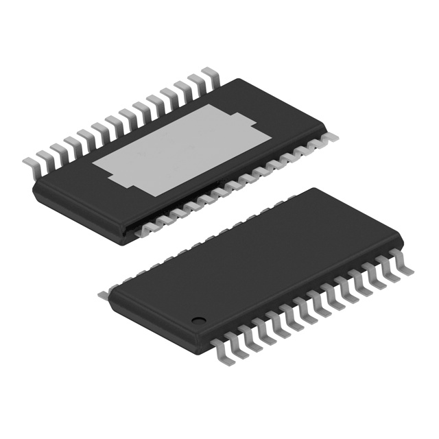
The DRV8824-Q1 is available in a 28-terminal
HTSSOP package with PowerPAD™ (Eco-friendly:
RoHS & no Sb/Br).
Device Information
Automotive HVAC
Automotive Valves
Automotive Infotainment
ORDER NUMBER
DRV8824QPWPRQ1
PACKAGE
HTSSOP (28)
BODY SIZE
9.7 mm x 4.4 mm
4 Simplified Schematic
8.2 to 45 V
Microstepping Current Waveform
M
1.6 A
-
Controller
DRV8824-Q1
+
STEP/DIR
Step size
Stepper
Motor Driver
+
Decay mode
1.6 A
-
Increasing
Current
Decreasing
Current
Increasing
Current
Decreasing
Current
1/32 µstep
1
An IMPORTANT NOTICE at the end of this data sheet addresses availability, warranty, changes, use in safety-critical applications,
intellectual property matters and other important disclaimers. PRODUCTION DATA.
�DRV8824-Q1
SLVSCH0 – APRIL 2014
www.ti.com
Table of Contents
1
2
3
4
5
6
7
8
Features ..................................................................
Applications ...........................................................
Description .............................................................
Simplified Schematic.............................................
Revision History.....................................................
Terminal Configuration and Functions................
Specifications.........................................................
1
1
1
1
2
3
4
7.1
7.2
7.3
7.4
7.5
7.6
7.7
4
4
4
5
5
6
8
Absolute Maximum Ratings ......................................
Handling Ratings.......................................................
Recommended Operating Conditions.......................
Thermal Information ..................................................
Electrical Characteristics...........................................
Timing Requirements ................................................
Typical Characteristics ..............................................
8.2 Functional Block Diagram ....................................... 10
8.3 Feature Description................................................. 11
8.4 Device Functional Modes........................................ 17
9
Application and Implementation ........................ 18
9.1 Application Information............................................ 18
9.2 Typical Application ................................................. 18
10 Power Supply Recommendations ..................... 20
11 Layout................................................................... 21
11.1 Layout Guidelines ................................................. 21
11.2 Layout Example .................................................... 21
12 Device and Documentation Support ................. 22
12.1 Trademarks ........................................................... 22
12.2 Electrostatic Discharge Caution ............................ 22
12.3 Glossary ................................................................ 22
13 Mechanical, Packaging, and Orderable
Information ........................................................... 22
Detailed Description .............................................. 9
8.1 Overview ................................................................... 9
5 Revision History
2
DATE
REVISION
NOTES
April 2014
*
Initial release.
Submit Documentation Feedback
Copyright © 2014, Texas Instruments Incorporated
�DRV8824-Q1
www.ti.com
SLVSCH0 – APRIL 2014
6 Terminal Configuration and Functions
PWP Package
(Top View)
Terminal Functions
NAME
TERMINAL
I/O
DESCRIPTION
EXTERNAL COMPONENTS
OR CONNECTIONS
POWER AND GROUND
GND
14, 28
-
Device ground
VMA
4
-
Bridge A power supply
VMB
11
-
Bridge B power supply
V3P3OUT
15
O
3.3-V regulator output
CP1
1
IO
Charge pump flying capacitor
CP2
2
IO
Charge pump flying capacitor
VCP
3
IO
High-side gate drive voltage
Connect a 0.1-μF 16-V ceramic capacitor and a 1-MΩ
resistor to VM.
nENBL
21
I
Enable input
Logic high to disable device outputs and indexer
operation, logic low to enable. Internal pulldown.
nSLEEP
17
I
Sleep mode input
Logic high to enable device, logic low to enter lowpower sleep mode. Internal pulldown.
STEP
22
I
Step input
Rising edge causes the indexer to move one step.
Internal pulldown.
DIR
20
I
Direction input
Level sets the direction of stepping. Internal pulldown.
MODE0
24
I
Microstep mode 0
MODE1
25
I
Microstep mode 1
MODE2
26
I
Microstep mode 2
DECAY
19
I
Decay mode
Low = slow decay, open = mixed decay,
high = fast decay. Internal pulldown and pullup.
nRESET
16
I
Reset input
Active-low reset input initializes the indexer logic and
disables the H-bridge outputs. Internal pulldown.
AVREF
12
I
Bridge A current set reference input
BVREF
13
I
Bridge B current set reference input
NC
23
Connect to motor supply (8.2 V - 45 V). Both terminals
must be connected to same supply.
Bypass to GND with a 0.47-μF 6.3-V ceramic
capacitor. Can be used to supply VREF.
Connect a 0.01-μF 50-V capacitor between CP1 and
CP2.
CONTROL
MODE0 - MODE2 set the step mode - full, 1/2, 1/4,
1/8/ 1/16, or 1/32 step. Internal pulldown.
Reference voltage for winding current set. Normally
AVREF and BVREF are connected to the same
voltage. Can be connected to V3P3OUT. A 0.01-µF
bypass capacitor to GND is recommended.
No connect
Leave this terminal unconnected.
STATUS
nHOME
27
OD
Home position
Logic low when at home state of step table
nFAULT
18
OD
Fault
Logic low when in fault condition (overtemp,
overcurrent)
Copyright © 2014, Texas Instruments Incorporated
Submit Documentation Feedback
3
�DRV8824-Q1
SLVSCH0 – APRIL 2014
www.ti.com
Terminal Functions (continued)
NAME
EXTERNAL COMPONENTS
OR CONNECTIONS
TERMINAL
I/O
DESCRIPTION
ISENA
6
IO
Bridge A ground / Isense
Connect to current sense resistor for bridge A.
ISENB
9
IO
Bridge B ground / Isense
Connect to current sense resistor for bridge B.
AOUT1
5
O
Bridge A output 1
AOUT2
7
O
Bridge A output 2
Connect to bipolar stepper motor winding A.
Positive current is AOUT1 → AOUT2
BOUT1
10
O
Bridge B output 1
BOUT2
8
O
Bridge B output 2
OUTPUT
Connect to bipolar stepper motor winding B.
Positive current is BOUT1 → BOUT2
7 Specifications
7.1 Absolute Maximum Ratings
over operating free-air temperature range (unless otherwise noted)
VMx
VREF
(1) (2)
VALUE
UNIT
Power supply voltage range
–0.3 to 47
V
Digital terminal voltage range
–0.5 to 7
V
Input voltage
ISENSEx terminal voltage
Peak motor drive output current, t < 1 μS
Continuous motor drive output current
(1)
(2)
(3)
V
V
Internally limited
A
1.6
A
(3)
Continuous total power dissipation
TJ
–0.3 to 4
–0.3 to 0.8
See Thermal Information table
Operating virtual junction temperature range
–40 to 150
°C
Stresses beyond those listed under absolute maximum ratings may cause permanent damage to the device. These are stress ratings
only, and functional operation of the device at these or any other conditions beyond those indicated under recommended operating
conditions is not implied. Exposure to absolute maximum rated conditions for extended periods may affect device reliability.
All voltage values are with respect to network ground terminal.
Power dissipation and thermal limits must be observed.
7.2 Handling Ratings
MIN
Tstg
Storage temperature range
VESD
–60
MAX
UNIT
150
°C
HBD (human body model), AEC-Q100 Classification H2
2000
CDM (charged device model), AEC-Q100 Classification C4B
750
V
7.3 Recommended Operating Conditions
MIN
VM
Motor power supply voltage
VREF
VREF input voltage (2)
IV3P3
V3P3OUT load current
(1)
(2)
4
(1)
NOM
MAX
8.2
45
1
3.5
1
UNIT
V
V
mA
All VM terminals must be connected to the same supply voltage.
Operational at VREF between 0 V and 1 V, but accuracy is degraded.
Submit Documentation Feedback
Copyright © 2014, Texas Instruments Incorporated
�DRV8824-Q1
www.ti.com
SLVSCH0 – APRIL 2014
7.4 Thermal Information
DRV8824-Q1
THERMAL METRIC
PWP
UNIT
28 TERMINAL
RθJA
Junction-to-ambient thermal resistance (1)
38.9
(2)
RθJC(top)
Junction-to-case (top) thermal resistance
RθJB
Junction-to-board thermal resistance (3)
21.2
ψJT
Junction-to-top characterization parameter (4)
0.8
ψJB
Junction-to-board characterization parameter (5)
20.9
RθJC(bot)
Junction-to-case (bottom) thermal resistance (6)
2.6
(1)
(2)
(3)
(4)
(5)
(6)
23.3
°C/W
The junction-to-ambient thermal resistance under natural convection is obtained in a simulation on a JEDEC-standard, high-K board, as
specified in JESD51-7, in an environment described in JESD51-2a.
The junction-to-case (top) thermal resistance is obtained by simulating a cold plate test on the package top. No specific JEDECstandard test exists, but a close description can be found in the ANSI SEMI standard G30-88.
The junction-to-board thermal resistance is obtained by simulating in an environment with a ring cold plate fixture to control the PCB
temperature, as described in JESD51-8.
The junction-to-top characterization parameter, ψJT, estimates the junction temperature of a device in a real system and is extracted
from the simulation data for obtaining θJA, using a procedure described in JESD51-2a (sections 6 and 7).
The junction-to-board characterization parameter, ψJB, estimates the junction temperature of a device in a real system and is extracted
from the simulation data for obtaining θJA , using a procedure described in JESD51-2a (sections 6 and 7).
The junction-to-case (bottom) thermal resistance is obtained by simulating a cold plate test on the exposed (power) pad. No specific
JEDEC standard test exists, but a close description can be found in the ANSI SEMI standard G30-88.
Spacer
7.5 Electrical Characteristics
over operating free-air temperature range of -40°C to 125°C (unless otherwise noted)
PARAMETER
TEST CONDITIONS
MIN
TYP
MAX
UNIT
5
8
mA
POWER SUPPLIES
IVM
VM operating supply current
VM = 24 V, fPWM < 50 kHz
IVMQ
VM sleep mode supply current
VM = 24 V
10
20
μA
VUVLO
VM undervoltage lockout voltage
VM rising
7.8
8.2
V
V3P3OUT REGULATOR
V3P3
V3P3OUT voltage
IOUT = 0 to 1 mA, VM = 24 V, TJ = 25°C
3.18
3.30
3.45
IOUT = 0 to 1 mA
3.10
3.30
3.50
0.6
0.7
V
5.25
V
20
μA
V
LOGIC-LEVEL INPUTS
VIL
Input low voltage
VIH
Input high voltage
VHYS
Input hysteresis
IIL
Input low current
VIN = 0
IIH
Input high current
VIN = 3.3 V
RPD
Internal pulldown resistance
2
0.45
–20
V
100
nENBL, nRESET, DIR, STEP, MODEx
nSLEEP
μA
100
kΩ
1
MΩ
nHOME, nFAULT OUTPUTS (OPEN-DRAIN OUTPUTS)
VOL
Output low voltage
IO = 5 mA
IOH
Output high leakage current
VO = 3.3 V
0.5
V
1
μA
0.8
V
100
µA
DECAY INPUT
VIL
Input low threshold voltage
For slow decay mode
VIH
Input high threshold voltage
For fast decay mode
IIN
Input current
RPU
Internal pullup resistance
RPD
Internal pulldown resistance
Copyright © 2014, Texas Instruments Incorporated
2
V
–100
130
kΩ
80
kΩ
Submit Documentation Feedback
5
�DRV8824-Q1
SLVSCH0 – APRIL 2014
www.ti.com
Electrical Characteristics (continued)
over operating free-air temperature range of -40°C to 125°C (unless otherwise noted)
PARAMETER
TEST CONDITIONS
MIN
TYP
MAX
UNIT
Ω
H-BRIDGE FETS
RDS(ON)
RDS(ON)
IOFF
HS FET on resistance
LS FET on resistance
VM = 24 V, I O = 1 A, TJ = 25°C
0.63
VM = 24 V, IO = 1 A, TJ = 85°C
0.76
0.90
VM = 24 V, IO = 1 A, TJ = 125°C
0.85
1
VM = 24 V, IO = 1 A, TJ = 25°C
0.65
VM = 24 V, IO = 1 A, TJ = 85°C
0.78
0.90
VM = 24 V, IO = 1 A, TJ = 125°C
0.85
1
Off-state leakage current
–20
20
Ω
μA
MOTOR DRIVER
fPWM
Internal PWM frequency
50
kHz
tBLANK
Current sense blanking time
tR
Rise time
VM = 24 V
100
360
ns
tF
Fall time
VM = 24 V
80
250
ns
tDEAD
Dead time
μs
3.75
400
ns
PROTECTION CIRCUITS
IOCP
Overcurrent protection trip level
tTSD
Thermal shutdown temperature
1.8
Die temperature
150
5
A
160
180
°C
3
μA
660
685
mV
CURRENT CONTROL
IREF
xVREF input current
xVREF = 3.3 V
VTRIP
xISENSE trip voltage
xVREF = 3.3 V, 100% current setting
Current trip accuracy
(relative to programmed value)
ΔITRIP
AISENSE
Current sense amplifier gain
–3
635
xVREF = 3.3 V , 5% current setting
–25%
25%
xVREF = 3.3 V , 10% - 34% current
setting
–15%
15%
xVREF = 3.3 V, 38% - 67% current
setting
–10%
10%
xVREF = 3.3 V, 71% - 100% current
setting
–5%
5%
Reference only
5
V/V
7.6 Timing Requirements
MIN
MAX
UNIT
250
kHz
1
fSTEP
Step frequency
2
tWH(STEP)
Pulse duration, STEP high
1.9
μs
3
tWL(STEP)
Pulse duration, STEP low
1.9
μs
4
tSU(STEP)
Setup time, command to STEP rising
200
ns
5
tH(STEP)
Hold time, command to STEP rising
200
ns
6
tENBL
Enable time, nENBL active to STEP
200
ns
7
tWAKE
Wakeup time, nSLEEP inactive to STEP
1
ms
6
Submit Documentation Feedback
Copyright © 2014, Texas Instruments Incorporated
�DRV8824-Q1
www.ti.com
SLVSCH0 – APRIL 2014
Figure 1. Timing Diagram
Copyright © 2014, Texas Instruments Incorporated
Submit Documentation Feedback
7
�DRV8824-Q1
SLVSCH0 – APRIL 2014
www.ti.com
7.7 Typical Characteristics
7.0
14
13
6.5
12
IVMQ (�A)
IVM (mA)
6.0
5.5
5.0
11
10
9
-40°C
8
25°C
4.5
85°C
125°C
4.0
10
15
20
25
30
35
40
VM (V)
25°C
85°C
7
125°C
6
45
10
15
C001
-40°C
85°C
25°C
125°C
35
40
45
C002
10 V
24 V
1800
RDS(ON) HS + LS (m)
RDS(ON) HS + LS (m)
30
Figure 3. IVMQ vs VM
2000
1800
1600
1400
1200
1000
45 V
1600
1400
1200
1000
800
800
10
15
20
25
30
35
VM (V)
Figure 4. RDS(ON) vs VM
8
25
VM (V)
Figure 2. IVM vs VM
2000
20
Submit Documentation Feedback
40
45
C003
±50
±25
0
25
50
75
TA (C)
100
125
C004
Figure 5. RDS(ON) vs Temperature
Copyright © 2014, Texas Instruments Incorporated
�DRV8824-Q1
www.ti.com
SLVSCH0 – APRIL 2014
8 Detailed Description
8.1 Overview
The DRV8824-Q1 is an integrated motor driver solution for bipolar stepper motors. The device integrates two
NMOS H-bridges, current sense and regulation circuitry, and a microstepping indexer. The DRV8824-Q1 can be
powered with a supply voltage between 8.2 V and 45 V, and is capable of providing an output current up to 1.6 A
full-scale or 1.1 A rms.
A simple STEP/DIR interface allows easy interfacing to the controller circuit. The internal indexer is able to
execute high-accuracy microstepping without requiring the processor to control the current level.
The current regulation is highly configurable, with three decay modes of operation. Fast, slow, and mixed decay
can be used.
A low-power sleep mode is included which allows the system to save power when not driving the motor.
Copyright © 2014, Texas Instruments Incorporated
Submit Documentation Feedback
9
�DRV8824-Q1
SLVSCH0 – APRIL 2014
www.ti.com
8.2 Functional Block Diagram
VM
3.3 V
LS Gate
Drive
V3P3OUT
CP1
Internal
VCC
V3P3OUT
Charge
Pump
Low Side
Gate
Drive
CP2
HS Gate
Drive
VM
VCP
3.3 V
VM
AVREF
VM
BVREF
VMA
+
nENBL
AOUT1
+
STEP
Stepper
Motor
Motor Driver
A
AOUT2
DIR
±
+
±
DECAY
ISENA
MODE0
MODE1
MODE2
Control
Logic/
Indexer
VM
VMB
nRESET
BOUT1
Motor Driver
B
nSLEEP
BOUT2
nHOME
Thermal
Shut
Down
nFAULT
GND
10
Submit Documentation Feedback
PPAD
ISENB
GND
Copyright © 2014, Texas Instruments Incorporated
�DRV8824-Q1
www.ti.com
SLVSCH0 – APRIL 2014
8.3 Feature Description
8.3.1 PWM Motor Drivers
The DRV8824-Q1 contains two H-bridge motor drivers with current-control PWM circuitry. A block diagram of the
motor control circuitry is shown in Figure 6.
Figure 6. Motor Control Circuitry
Note that there are multiple VM motor power supply terminals. All VM terminals must be connected together to
the motor supply voltage.
Copyright © 2014, Texas Instruments Incorporated
Submit Documentation Feedback
11
�DRV8824-Q1
SLVSCH0 – APRIL 2014
www.ti.com
Feature Description (continued)
8.3.2 Current Regulation
The current through the motor windings is regulated by a fixed-frequency PWM current regulation, or current
chopping. When an H-bridge is enabled, current rises through the winding at a rate dependent on the DC voltage
and inductance of the winding. Once the current hits the current chopping threshold, the bridge disables the
current until the beginning of the next PWM cycle.
In stepping motors, current regulation is used to vary the current in the two windings in a semi-sinusoidal fashion
to provide smooth motion.
The PWM chopping current is set by a comparator which compares the voltage across a current sense resistor
connected to the xISEN terminals, multiplied by a factor of 5, with a reference voltage. The reference voltage is
input from the xVREF terminals.
The full-scale (100%) chopping current is calculated in Equation 1.
VREFX
ICHOP = 5¾
· RISENSE
(1)
Example:
If a 0.5-Ω sense resistor is used and the VREFx terminal is 3.3 V, the full-scale (100%) chopping current will
be 3.3 V / (5 x 0.5 Ω) = 1.32 A.
The reference voltage is scaled by an internal DAC that allows fractional stepping of a bipolar stepper motor, as
described in the microstepping indexer section below.
8.3.3 Blanking Time
After the current is enabled in an H-bridge, the voltage on the xISEN terminal is ignored for a fixed period of time
before enabling the current sense circuitry. This blanking time is fixed at 3.75 μs. Note that the blanking time also
sets the minimum on time of the PWM.
8.3.4 Microstepping Indexer
Built-in indexer logic in the DRV8824-Q1 allows a number of different stepping configurations. The MODE0 MODE2 terminals are used to configure the stepping format as shown in .
Table 1. Stepping Format
MODE2
MODE1
MODE0
0
0
0
Full step (2-phase excitation) with 71% current
STEP MODE
0
0
1
1/2 step (1-2 phase excitation)
0
1
0
1/4 step (W1-2 phase excitation)
0
1
1
8 microsteps / step
1
0
0
16 microsteps / step
1
0
1
32 microsteps / step
1
1
0
32 microsteps / step
1
1
1
32 microsteps / step
Table 2 shows the relative current and step directions for different settings of MODEx. At each rising edge of the
STEP input, the indexer travels to the next state in the table. The direction is shown with the DIR terminal high; if
the DIR terminal is low the sequence is reversed. Positive current is defined as xOUT1 = positive with respect to
xOUT2.
Note that if the step mode is changed while stepping, the indexer will advance to the next valid state for the new
MODEx setting at the rising edge of STEP.
The home state is 45°. This state is entered at power-up or application of nRESET. This is shown in Table 2 by
the shaded cells. The logic inputs DIR, STEP, nRESET and MODEx have an internal pulldown resistors of
100 kΩ
12
Submit Documentation Feedback
Copyright © 2014, Texas Instruments Incorporated
�DRV8824-Q1
www.ti.com
SLVSCH0 – APRIL 2014
Table 2. Relative Current and Step Directions
1/32 STEP 1/16 STEP
1
1
1/8 STEP
1/4 STEP
1/2 STEP
1
1
1
FULL
STEP
70%
2
3
2
4
5
3
2
6
7
4
8
9
5
3
2
10
11
6
12
13
7
4
14
15
8
16
17
9
5
3
2
18
19
10
20
21
11
6
22
23
12
24
25
13
7
4
26
27
14
28
29
15
8
30
31
16
32
33
17
9
5
34
35
18
36
37
19
10
38
39
20
40
41
21
11
42
43
22
44
45
23
12
46
Copyright © 2014, Texas Instruments Incorporated
6
3
1
WINDING
CURRENT
A
WINDING
CURRENT
B
ELECTRICAL
ANGLE
100%
0%
0
100%
5%
3
100%
10%
6
99%
15%
8
98%
20%
11
97%
24%
14
96%
29%
17
94%
34%
20
92%
38%
23
90%
43%
25
88%
47%
28
86%
51%
31
83%
56%
34
80%
60%
37
77%
63%
39
74%
67%
42
71%
71%
45
67%
74%
48
63%
77%
51
60%
80%
53
56%
83%
56
51%
86%
59
47%
88%
62
43%
90%
65
38%
92%
68
34%
94%
70
29%
96%
73
24%
97%
76
20%
98%
79
15%
99%
82
10%
100%
84
5%
100%
87
0%
100%
90
–5%
100%
93
–10%
100%
96
–15%
99%
98
–20%
98%
101
–24%
97%
104
–29%
96%
107
–34%
94%
110
–38%
92%
113
–43%
90%
115
–47%
88%
118
–51%
86%
121
–56%
83%
124
–60%
80%
127
Submit Documentation Feedback
13
�DRV8824-Q1
SLVSCH0 – APRIL 2014
www.ti.com
Table 2. Relative Current and Step Directions (continued)
1/32 STEP 1/16 STEP
47
1/8 STEP
1/4 STEP
1/2 STEP
FULL
STEP
70%
24
48
49
25
13
7
4
2
50
51
26
52
53
27
14
54
55
28
56
57
29
15
8
58
59
30
60
61
31
16
62
63
32
64
65
33
17
9
5
66
67
34
68
69
35
18
70
71
36
72
73
37
19
10
74
75
38
76
77
39
20
78
79
40
80
81
41
21
11
82
83
42
84
85
43
22
86
87
44
88
89
45
23
90
91
46
92
14
Submit Documentation Feedback
12
6
3
WINDING
CURRENT
A
WINDING
CURRENT
B
ELECTRICAL
ANGLE
–63%
77%
129
–67%
74%
132
–71%
71%
135
–74%
67%
138
–77%
63%
141
–80%
60%
143
–83%
56%
146
–86%
51%
149
–88%
47%
152
–90%
43%
155
–92%
38%
158
–94%
34%
160
–96%
29%
163
–97%
24%
166
–98%
20%
169
–99%
15%
172
–100%
10%
174
–100%
5%
177
–100%
0%
180
–100%
–5%
183
–100%
–10%
186
–99%
–15%
188
–98%
–20%
191
–97%
–24%
194
–96%
–29%
197
–94%
–34%
200
–92%
–38%
203
–90%
–43%
205
–88%
–47%
208
–86%
–51%
211
–83%
–56%
214
–80%
–60%
217
–77%
–63%
219
–74%
–67%
222
–71%
–71%
225
–67%
–74%
228
–63%
–77%
231
–60%
–80%
233
–56%
–83%
236
–51%
–86%
239
–47%
–88%
242
–43%
–90%
245
–38%
–92%
248
–34%
–94%
250
–29%
–96%
253
–24%
–97%
256
Copyright © 2014, Texas Instruments Incorporated
�DRV8824-Q1
www.ti.com
SLVSCH0 – APRIL 2014
Table 2. Relative Current and Step Directions (continued)
1/32 STEP 1/16 STEP
93
47
1/8 STEP
1/4 STEP
1/2 STEP
FULL
STEP
70%
24
94
95
48
96
97
49
25
13
7
98
99
50
100
101
51
26
102
103
52
104
105
53
27
14
106
107
54
108
109
55
28
110
111
56
112
113
57
29
15
8
114
115
58
116
117
59
30
118
119
60
120
121
61
31
16
122
123
62
124
125
63
32
126
127
64
128
4
WINDING
CURRENT
A
WINDING
CURRENT
B
ELECTRICAL
ANGLE
–20%
–98%
259
–15%
–99%
262
–10%
–100%
264
–5%
–100%
267
0%
–100%
270
5%
–100%
273
10%
–100%
276
15%
–99%
278
20%
–98%
281
24%
–97%
284
29%
–96%
287
34%
–94%
290
38%
–92%
293
43%
–90%
295
47%
–88%
298
51%
–86%
301
56%
–83%
304
60%
–80%
307
63%
–77%
309
67%
–74%
312
71%
–71%
315
74%
–67%
318
77%
–63%
321
80%
–60%
323
83%
–56%
326
86%
–51%
329
88%
–47%
332
90%
–43%
335
92%
–38%
338
94%
–34%
340
96%
–29%
343
97%
–24%
346
98%
–20%
349
99%
–15%
352
100%
–10%
354
100%
–5%
357
8.3.5 nRESET, nENBLE and nSLEEP Operation
The nRESET terminal, when driven active low, resets internal logic, and resets the step table to the home
position. It also disables the H-bridge drivers. The STEP input is ignored while nRESET is active.
The nENBL terminal is used to control the output drivers and enable/disable operation of the indexer. When
nENBL is low, the output H-bridges are enabled, and rising edges on the STEP terminal are recognized. When
nENBL is high, the H-bridges are disabled, the outputs are in a high-impedance state, and the STEP input is
ignored.
Copyright © 2014, Texas Instruments Incorporated
Submit Documentation Feedback
15
�DRV8824-Q1
SLVSCH0 – APRIL 2014
www.ti.com
Driving nSLEEP low will put the device into a low power sleep state. In this state, the H-bridges are disabled, the
gate drive charge pump is stopped, the V3P3OUT regulator is disabled, and all internal clocks are stopped. In
this state all inputs are ignored until nSLEEP returns inactive high. When returning from sleep mode, some time
(approximately 1 ms) needs to pass before applying a STEP input, to allow the internal circuitry to stabilize.
The nRESET and nENABLE terminals have internal pulldown resistors of 100 kΩ. The nSLEEP terminal has an
internal pulldown resistor of 1 MΩ.
8.3.6 Protection Circuits
The DRV8824-Q1 is fully protected against undervoltage, overcurrent and overtemperature events.
8.3.6.1 Overcurrent Protection (OCP)
An analog current limit circuit on each FET limits the current through the FET by removing the gate drive. If this
analog current limit persists for longer than the OCP time, all FETs in the H-bridge will be disabled and the
nFAULT terminal will be driven low. The device will remain disabled until either nRESET terminal is applied, or
VM is removed and re-applied.
Overcurrent conditions on both high and low side devices; i.e., a short to ground, supply, or across the motor
winding will all result in an overcurrent shutdown. Note that overcurrent protection does not use the current sense
circuitry used for PWM current control, and is independent of the ISENSE resistor value or VREF voltage.
8.3.6.2 Thermal Shutdown (TSD)
If the die temperature exceeds safe limits, all FETs in the H-bridge will be disabled and the nFAULT terminal will
be driven low. Once the die temperature has fallen to a safe level operation will automatically resume.
8.3.6.3 Undervoltage Lockout (UVLO)
If at any time the voltage on the VM terminals falls below the undervoltage lockout threshold voltage, all circuitry
in the device will be disabled and internal logic will be reset. Operation will resume when VM rises above the
UVLO threshold.
8.3.7 Thermal Information
8.3.7.1 Thermal Protection
The DRV8824-Q1 has thermal shutdown (TSD) as described above. If the die temperature exceeds
approximately 150°C, the device will be disabled until the temperature drops to a safe level.
Any tendency of the device to enter TSD is an indication of either excessive power dissipation, insufficient
heatsinking, or too high an ambient temperature.
8.3.7.2 Power Dissipation
Power dissipation in the DRV8824-Q1 is dominated by the power dissipated in the output FET resistance, or
RDS(ON). Average power dissipation when running a stepper motor can be roughly estimated by Equation 2.
PTOT = 4 · RDS(ON) · (IOUT(RMS))
2
(2)
where PTOT is the total power dissipation, RDS(ON) is the resistance of each FET, and IOUT(RMS) is the RMS output
current being applied to each winding. IOUT(RMS) is equal to the approximately 0.7x the full-scale output current
setting. The factor of 4 comes from the fact that there are two motor windings, and at any instant two FETs are
conducting winding current for each winding (one high-side and one low-side).
The maximum amount of power that can be dissipated in the device is dependent on ambient temperature and
heatsinking.
Note that RDS(ON) increases with temperature, so as the device heats, the power dissipation increases. This must
be taken into consideration when sizing the heatsink.
16
Submit Documentation Feedback
Copyright © 2014, Texas Instruments Incorporated
�DRV8824-Q1
www.ti.com
SLVSCH0 – APRIL 2014
8.3.7.3 Heatsinking
The PowerPAD™ package uses an exposed pad to remove heat from the device. For proper operation, this pad
must be thermally connected to copper on the PCB to dissipate heat. On a multi-layer PCB with a ground plane,
this can be accomplished by adding a number of vias to connect the thermal pad to the ground plane. On PCBs
without internal planes, copper area can be added on either side of the PCB to dissipate heat. If the copper area
is on the opposite side of the PCB from the device, thermal vias are used to transfer the heat between top and
bottom layers.
For details about how to design the PCB, refer to TI application report SLMA002, "PowerPAD™ Thermally
Enhanced Package" and TI application brief SLMA004, "PowerPAD™ Made Easy", available at www.ti.com.
In general, the more copper area that can be provided, the more power can be dissipated. It can be seen that the
heatsink effectiveness increases rapidly to about 20 cm2, then levels off somewhat for larger areas.
8.4 Device Functional Modes
8.4.1 Decay Mode
During PWM current chopping, the H-bridge is enabled to drive current through the motor winding until the PWM
current chopping threshold is reached. This is shown in Figure 7 as case 1. The current flow direction shown
indicates positive current flow.
Once the chopping current threshold is reached, the H-bridge can operate in two different states, fast decay or
slow decay.
In fast decay mode, once the PWM chopping current level has been reached, the H-bridge reverses state to
allow winding current to flow in a reverse direction. As the winding current approaches zero, the bridge is
disabled to prevent any reverse current flow. Fast decay mode is shown in Figure 7 as case 2.
In slow decay mode, winding current is re-circulated by enabling both of the low-side FETs in the bridge. This is
shown in Figure 7 as case 3.
Figure 7. Decay Mode
The DRV8824-Q1 supports fast decay, slow decay and a mixed decay mode. Slow, fast, or mixed decay mode is
selected by the state of the DECAY terminal - logic low selects slow decay, open selects mixed decay operation,
and logic high sets fast decay mode. The DECAY terminal has both an internal pullup resistor of approximately
130 kΩ and an internal pulldown resistor of approximately 80 kΩ. This sets the mixed decay mode if the terminal
is left open or undriven.
Copyright © 2014, Texas Instruments Incorporated
Submit Documentation Feedback
17
�DRV8824-Q1
SLVSCH0 – APRIL 2014
www.ti.com
Device Functional Modes (continued)
Mixed decay mode begins as fast decay, but at a fixed period of time (75% of the PWM cycle) switches to slow
decay mode for the remainder of the fixed PWM period. This occurs only if the current through the winding is
decreasing (per the indexer step table); if the current is increasing, then slow decay is used.
9 Application and Implementation
9.1 Application Information
The DRV8824-Q1 is used in bipolar stepper control. The following design procedure can be used to configure the
DRV8824-Q1.
9.2 Typical Application
DRV8824-Q1
1
0.01 µF
VM
28
CP1
GND
CP2
nHOME
VCP
MODE2
VMA
MODE1
2
27
3
0.01 µF
1 MΩ
0.1 µF
26
4
MODE0
6
400 mΩ
NC
22
AOUT2
STEP
BOUT2
nENBL
8
-
21
9
400 mΩ
20
ISENB
DIR
10
19
BOUT1
DECAY
11
VM
18
VMB
nFAULT
AVREF
nSLEEP
12
+
0.01 µF
V3P3
23
ISENA
7
+
24
AOUT1
+
Step
Motor
10 kΩ
25
5
17
13
10 kΩ
16
BVREF
nRESET
14
15
GND
V3P3OUT
10 kΩ
0.47 µF
30 kΩ
Figure 8. Typical Application Schematic
9.2.1 Design Requirements
Table 3 gives design input parameters for system design.
Table 3. Design Parameters
DESIGN PARAMETER
REFERENCE
EXAMPLE VALUE
Supply voltage
VM
Motor winding resistance
RL
1.0 Ω/phase
Motor winding inductance
LL
3.5 mH/phase
θstep
1.8°/step
nm
8 microsteps per step
v
120 rpm
IFS
1.25 A
Motor full step angle
Target microstepping level
Target motor speed
Target full-scale current
18
Submit Documentation Feedback
24 V
Copyright © 2014, Texas Instruments Incorporated
�DRV8824-Q1
www.ti.com
SLVSCH0 – APRIL 2014
9.2.2 Detailed Design Procedure
9.2.2.1 Stepper Motor Speed
The first step in configuring the DRV8824-Q1 requires the desired motor speed and microstepping level. If the
target application requires a constant speed, then a square wave with frequency fstep must be applied to the
STEP pin.
If the target motor speed is too high, the motor will not spin. Make sure that the motor can support the target
speed.
For a desired motor speed (v), microstepping level (nm), and motor full step angle (θstep),
v(rpm) · nm(steps) · 6
fstep(step/sec) = ¾
qstep(°/step)
(3)
θstep can be found in the stepper motor datasheet or written on the motor itself.
For the DRV8824-Q1, the microstepping level is set by the USM pins and can be any of the settings in . Higher
microstepping will mean a smother motor motion and less audible noise, but will increase switching losses and
require a higher fstep to achieve the same motor speed.
9.2.2.2 Current Regulation
In a stepper motor, the full-scale current (IFS) is the maximum current driven through either winding. This quantity
will depend on the VREF analog voltage and the sense resistor value (RSENSE). During stepping, IFS defines the
current chopping threshold (ITRIP) for the maximum current step.
VREF(V)
VREF(V)
¾
IFS(A) = ¾
=
5 · RSENSE(W)
Av · RSENSE(W)
(4)
IFS is set by a comparator which compares the voltage across RSENSE to a reference voltage. There is a current
sense amplifier built in with programmable gain through ISGAIN. Note that IFS must also follow the equation
below in order to avoid saturating the motor. VM is the motor supply voltage and RL is the motor winding
resistance.
IFS(A) <
VM(V)
¾
RL(W) + 2 · RDS(ON)(W) + RSENSE(W)
(5)
9.2.2.3 Decay Modes
The DRV8824-Q1 supports three different decay modes: slow decay, fast decay, and mixed decay. The current
through the motor windings is regulated using a fixed-frequency PWM scheme. This means that after any drive
phase, when a motor winding current has hit the current chopping threshold (ITRIP), the DRV8824-Q1 will place
the winding in one of the three decay modes until the PWM cycle has expired. Afterwards, a new drive phase
starts.
The blanking time tBLANK defines the minimum drive time for the current chopping. ITRIP is ignored during tBLANK,
so the winding current may overshoot the trip level.
Copyright © 2014, Texas Instruments Incorporated
Submit Documentation Feedback
19
�DRV8824-Q1
SLVSCH0 – APRIL 2014
www.ti.com
9.2.3 Application Curves
Figure 9. Microstepping Waveform, Phase A, Mixed Decay
Figure 10. Microstepping Waveform, Slow Decay on
Increasing Steps
Figure 11. Microstepping Waveform, Mixed Decay on Decreasing Steps
10 Power Supply Recommendations
The DRV8824-Q1 is designed to operate from an input voltage supply (VM) range between 8.2 V and 45 V. Two
0.01-µF ceramic capacitorS rated for VMA and VMB must be placed as close to the DRV8824-Q1 as possible. In
addition, a bulk capacitor must be included. If VMA and VMB are connected to the same board net, a single bulk
capacitor is sufficient.
20
Submit Documentation Feedback
Copyright © 2014, Texas Instruments Incorporated
�DRV8824-Q1
www.ti.com
SLVSCH0 – APRIL 2014
11 Layout
11.1 Layout Guidelines
The VMA and VMB terminals should be bypassed to GND using low-ESR ceramic bypass capacitors with a
recommended value of 0.01 µF rated for VM. This capacitor should be placed as close to the VMA and VMB pins
as possible with a thick trace or ground plane connection to the device GND pin.
The VMA and VMB pins must be bypassed to ground using a bulk capacitor. This component may be an
electrolytic. If VMA and VMB are connected to the same board net, a single bulk capacitor is sufficient.
A low-ESR ceramic capacitor must be placed in between the CPL and CPH pins. A value of 0.01 µF rated for
VMA and VMB is recommended. Place this component as close to the pins as possible.
A low-ESR ceramic capacitor must be placed in between the VMA and VCP pins. A value of 0.1 µF rated for 16
V is recommended. Place this component as close to the pins as possible. In addition place a 1-MΩ resistor
between VCP and VMA.
Bypass V3P3 to ground with a ceramic capacitor rated 6.3 V. Place this bypassing capacitor as close to the pin
as possible.
11.2 Layout Example
0.01 µF
CP1
GND
CP2
nHOME
VCP
MODE2
VMA
MODE1
AOUT1
MODE0
ISENA
NC
AOUT2
STEP
BOUT2
nEMBL
ISENB
DIR
BOUT1
DECAY
VMB
nFAULT
AVREF
nSLEEP
BVREF
nRESET
GND
V3P3OUT
0.01 µF
1 MΩ
0.1 µF
RISENA
RISENB
+
0.01 µF
0.47 µF
Figure 12. DRV8824-Q1 Board Layout
Copyright © 2014, Texas Instruments Incorporated
Submit Documentation Feedback
21
�DRV8824-Q1
SLVSCH0 – APRIL 2014
www.ti.com
12 Device and Documentation Support
12.1 Trademarks
PowerPAD is a trademark of Texas Instruments.
All other trademarks are the property of their respective owners.
12.2 Electrostatic Discharge Caution
These devices have limited built-in ESD protection. The leads should be shorted together or the device placed in conductive foam
during storage or handling to prevent electrostatic damage to the MOS gates.
12.3 Glossary
SLYZ022 — TI Glossary.
This glossary lists and explains terms, acronyms and definitions.
13 Mechanical, Packaging, and Orderable Information
The following pages include mechanical, packaging, and orderable information. This information is the most
current data available for the designated devices. This data is subject to change without notice and revision of
this document. For browser-based versions of this data sheet, refer to the left-hand navigation.
22
Submit Documentation Feedback
Copyright © 2014, Texas Instruments Incorporated
�PACKAGE OPTION ADDENDUM
www.ti.com
10-Dec-2020
PACKAGING INFORMATION
Orderable Device
Status
(1)
Package Type Package Pins Package
Drawing
Qty
Eco Plan
(2)
Lead finish/
Ball material
MSL Peak Temp
Op Temp (°C)
(3)
Device Marking
(4/5)
(6)
DRV8824QPWPRQ1
ACTIVE
HTSSOP
PWP
28
2000
RoHS & Green
NIPDAU
Level-3-260C-168 HR
-40 to 125
DRV8824Q1
(1)
The marketing status values are defined as follows:
ACTIVE: Product device recommended for new designs.
LIFEBUY: TI has announced that the device will be discontinued, and a lifetime-buy period is in effect.
NRND: Not recommended for new designs. Device is in production to support existing customers, but TI does not recommend using this part in a new design.
PREVIEW: Device has been announced but is not in production. Samples may or may not be available.
OBSOLETE: TI has discontinued the production of the device.
(2)
RoHS: TI defines "RoHS" to mean semiconductor products that are compliant with the current EU RoHS requirements for all 10 RoHS substances, including the requirement that RoHS substance
do not exceed 0.1% by weight in homogeneous materials. Where designed to be soldered at high temperatures, "RoHS" products are suitable for use in specified lead-free processes. TI may
reference these types of products as "Pb-Free".
RoHS Exempt: TI defines "RoHS Exempt" to mean products that contain lead but are compliant with EU RoHS pursuant to a specific EU RoHS exemption.
Green: TI defines "Green" to mean the content of Chlorine (Cl) and Bromine (Br) based flame retardants meet JS709B low halogen requirements of


 工商网监
湘ICP备2023018690号
工商网监
湘ICP备2023018690号
