DRV8824
SLVSA06K – OCTOBER 2009 – REVISED JANUARY 2022
DRV8824 Stepper Motor Controller IC
1 Features
3 Description
•
The DRV8824 provides an integrated motor driver
solution for printers, scanners, and other automated
equipment applications. The device has two Hbridge drivers and a microstepping indexer, and
is intended to drive a bipolar stepper motor. The
output driver block consists of N-channel power
MOSFETs configured as full H-bridges to drive the
motor windings. The DRV8824 is capable of driving
up to 1.6 A of current from each output (with proper
heatsinking, at 24 V and 25°C).
•
•
•
•
•
•
•
•
PWM Microstepping Stepper Motor Driver
– Built-In Microstepping Indexer
– Up to 1/32 Microstepping
Multiple Decay Modes:
– Mixed Decay
– Slow Decay
– Fast Decay
8.2-V to 45-V Operating Supply Voltage Range
1.6-A Maximum Drive Current at 24 V and
TA = 25°C
Simple STEP/DIR Interface
Low-Current Sleep Mode
Built-In 3.3-V Reference Output
Small Package and Footprint
Protection Features:
– Overcurrent Protection (OCP)
– Thermal Shutdown (TSD)
– VMx Undervoltage Lockout (UVLO)
– Fault Condition Indication Pin (nFAULT)
A simple STEP/DIR interface allows easy interfacing
to controller circuits. Mode pins allow for configuration
of the motor in full-step up to 1/32-step modes. Decay
mode is configurable so that slow decay, fast decay,
or mixed decay can be used. A low-power sleep
mode is provided which shuts down internal circuitry
to achieve very-low quiescent current draw. This sleep
mode can be set using a dedicated nSLEEP pin.
Internal shutdown functions are provided for
overcurrent, short circuit, undervoltage lockout, and
over temperature. Fault conditions are indicated
through the nFAULT pin.
2 Applications
Automatic Teller Machines
Money Handling Machines
Video Security Cameras
Printers
Scanners
Office Automation Machines
Gaming Machines
Factory Automation
Robotics
Device Information(1)
PART NUMBER
DRV8824
(1)
PACKAGE
BODY SIZE (NOM)
HTSSOP (28)
9.70 mm × 6.40 mm
VQFN (28)
5.00 mm × 5.00 mm
For all available packages, see the orderable addendum at
the end of the data sheet.
8.2 to 45 V
DRV8824
DIR
Step Size
M
1.6 A
±
Decay Mode
Output Current
+
STEP
Controller
•
•
•
•
•
•
•
•
•
Stepper Motor
Driver
+
±
nFAULT
1.6 A
1/32 µstep
Simplified Schematic
STEP Input
Microstepping Current Waveform
An IMPORTANT NOTICE at the end of this data sheet addresses availability, warranty, changes, use in safety-critical applications,
intellectual property matters and other important disclaimers. PRODUCTION DATA.
�DRV8824
www.ti.com
SLVSA06K – OCTOBER 2009 – REVISED JANUARY 2022
Table of Contents
1 Features............................................................................1
2 Applications..................................................................... 1
3 Description.......................................................................1
4 Revision History.............................................................. 2
5 Pin Configuration and Functions...................................3
6 Specifications.................................................................. 5
6.1 Absolute Maximum Ratings........................................ 5
6.2 ESD Ratings............................................................... 5
6.3 Recommended Operating Conditions.........................5
6.4 Thermal Information....................................................5
6.5 Electrical Characteristics.............................................6
6.6 Timing Requirements.................................................. 7
6.7 Typical Characteristics................................................ 8
7 Detailed Description........................................................9
7.1 Overview..................................................................... 9
7.2 Functional Block Diagram......................................... 10
7.3 Feature Description...................................................11
7.4 Device Functional Modes..........................................17
8 Application and Implementation.................................. 18
8.1 Application Information............................................. 18
8.2 Typical Application.................................................... 18
9 Layout.............................................................................22
9.1 Layout Guidelines..................................................... 22
9.2 Layout Example........................................................ 22
9.3 Thermal Considerations............................................22
9.4 Power Dissipation..................................................... 23
9.5 Heatsinking............................................................... 23
10 Device and Documentation Support..........................24
10.1 Community Resources............................................24
10.2 Trademarks............................................................. 24
11 Mechanical, Packaging, and Orderable
Information.................................................................... 24
4 Revision History
NOTE: Page numbers for previous revisions may differ from page numbers in the current version.
Changes from Revision J (July 2014) to Revision K (January 2022)
Page
• Updated RHD pinout ..........................................................................................................................................3
• Added additional external component to connect to the VCP pin ......................................................................3
• Updated the Handling Ratings table to and ESD Ratings table and moved Tstg to the Absolute Maximum
Ratings table.......................................................................................................................................................5
• Corrected device part number ......................................................................................................................... 19
• Added Section 10.1 ......................................................................................................................................... 24
Changes from Revision I (June 2014) to Revision J (July 2014)
Page
• Updated images on the front page .................................................................................................................... 1
• Update the continuous motor drive output current value in Absolute Maximum Ratings .................................. 5
• Updated typical tDEG time .................................................................................................................................. 6
• Updated text and equations in Section 8.2.2 ................................................................................................... 19
• Updated Section 9.1 and image....................................................................................................................... 21
• Layout Example image updated. ..................................................................................................................... 22
Changes from Revision H (December 2013) to Revision I (June 2014)
Page
• Updated data sheet to new TI standard: added sections and rearranged material ........................................... 1
• Updated pin description for AVREF and BVREF ............................................................................................... 3
• Added power supply ramp rate to Absolute Maximum Ratings ......................................................................... 5
• Added minimum voltage for VIL and removed typical......................................................................................... 6
• Updated parameter descriptions in Timing Requirements and tWAKE minimum and maximum .........................7
Changes from Revision G (August 2013) to Revision H (December 2013)
Page
• Changed in Electrical Characteristics table, section DECAY INPUT third row................................................... 6
2
Submit Document Feedback
Copyright © 2022 Texas Instruments Incorporated
Product Folder Links: DRV8824
�DRV8824
www.ti.com
SLVSA06K – OCTOBER 2009 – REVISED JANUARY 2022
5 Pin Configuration and Functions
Figure 5-1. PWP Package 28-Pin HTSSOP Top View
DECAY
DIR
nENBL
STEP
NC
MODE0
MODE1
22
23
24
25
26
27
28
MODE2
nHOME
GND
CP1
CP2
VCP
VMA
1
21
2
20
3
19
GND
(PPAD)
4
18
5
17
6
16
7
15
nFAULT
nSLEEP
nRESET
V3P3OUT
GND
BVREF
AVREF
14
13
12
11
10
9
8
VMB
BOUT1
ISENB
BOUT2
AOUT2
ISENA
AOUT1
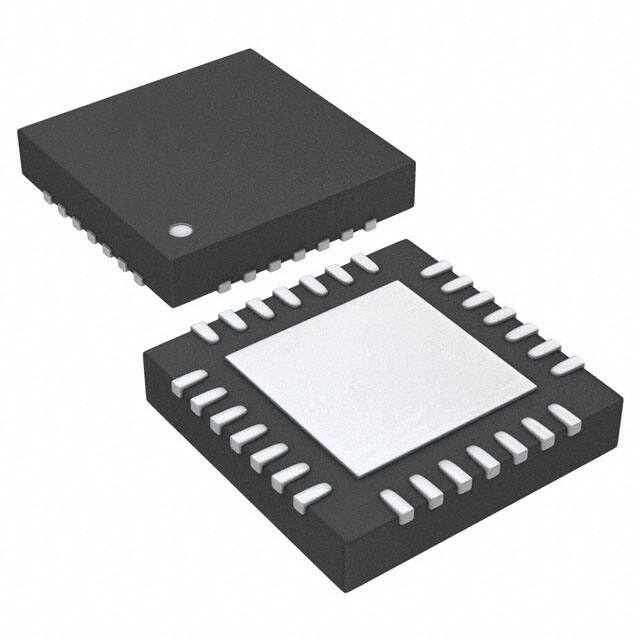
Figure 5-2. RHD Package 28-Pin VQFN Top View
Table 5-1. Pin Functions
PIN
NAME
PWP
RHD
I/O(1)
DESCRIPTION
EXTERNAL COMPONENTS OR CONNECTIONS
POWER AND GROUND
GND
14, 28
3, 17
—
Device ground
VMA
4
7
—
Bridge A power supply
VMB
11
14
—
Bridge B power supply
V3P3OUT
15
18
O
3.3-V regulator output
CP1
1
4
IO
Charge pump flying
capacitor
CP2
2
5
IO
Charge pump flying
capacitor
Connect to motor supply (8.2 to 45 V). Both pins must be
connected to same supply, bypassed with a 0.1-µF capacitor to
GND, and connected to appropriate bulk capacitance.
Bypass to GND with a 0.47-μF 6.3-V ceramic capacitor. Can
be used to supply VREF.
Connect a 0.01-μF 50-V capacitor between CP1 and CP2.
Submit Document Feedback
Copyright © 2022 Texas Instruments Incorporated
Product Folder Links: DRV8824
3
�DRV8824
www.ti.com
SLVSA06K – OCTOBER 2009 – REVISED JANUARY 2022
Table 5-1. Pin Functions (continued)
PIN
NAME
I/O(1)
DESCRIPTION
EXTERNAL COMPONENTS OR CONNECTIONS
PWP
RHD
3
6
IO
nENBL
21
24
I
Enable input
Logic high to disable device outputs and indexer operation,
logic low to enable. Internal pulldown.
nSLEEP
17
20
I
Sleep mode input
Logic high to enable device, logic low to enter low-power sleep
mode. Internal pulldown.
STEP
22
25
I
Step input
Rising edge causes the indexer to move one step. Internal
pulldown.
DIR
20
23
I
Direction input
Level sets the direction of stepping. Internal pulldown.
MODE0
24
27
I
Microstep mode 0
MODE1
25
28
I
Microstep mode 1
MODE2
26
1
I
Microstep mode 2
DECAY
19
22
I
Decay mode
Low = slow decay, Open = mixed decay,
High = fast decay. Internal pulldown and pullup.
nRESET
16
19
I
Reset input
Active-low reset input initializes the indexer logic and disables
the H-bridge outputs. Internal pulldown.
AVREF
12
15
I
Bridge A current set
reference input
BVREF
13
16
I
Bridge B current set
reference input
NC
23
26
—
No connect
Leave this pin unconnected.
nHOME
27
2
OD
Home position
Logic low when at home state of step table
nFAULT
18
21
OD
Fault
Logic low when in fault condition (overtemperature,
overcurrent)
VCP
Connect a 0.1-μF 16-V ceramic capacitor. A 1-MΩ resistor
High-side gate drive voltage can be connected to VM to accelerate discharge of the VCP
capacitor.
CONTROL
MODE0 through MODE2 set the step mode: full, 1/2, 1/4, 1/8/
1/16, or 1/32 step. Internal pulldown.
Reference voltage for winding current set. Normally AVREF
and BVREF are connected to the same voltage. Can be
connected to V3P3OUT.
STATUS
OUTPUT
ISENA
6
9
IO
Bridge A ground / Isense
Connect to current sense resistor for bridge A.
ISENB
9
12
IO
Bridge B ground / Isense
Connect to current sense resistor for bridge B.
AOUT1
5
8
O
Bridge A output 1
AOUT2
7
10
O
Bridge A output 2
Connect to bipolar stepper motor winding A.
Positive current is AOUT1 → AOUT2
BOUT1
10
13
O
Bridge B output 1
BOUT2
8
11
O
Bridge B output 2
(1)
4
Connect to bipolar stepper motor winding B.
Positive current is BOUT1 → BOUT2
Directions: I = input, O = output, OD = open-drain output, IO = input/output
Submit Document Feedback
Copyright © 2022 Texas Instruments Incorporated
Product Folder Links: DRV8824
�DRV8824
www.ti.com
SLVSA06K – OCTOBER 2009 – REVISED JANUARY 2022
6 Specifications
6.1 Absolute Maximum Ratings
over operating free-air temperature (unless otherwise noted) (1) (2)
V(VMx)
Power supply voltage
V(VMx)
Power supply ramp rate
V(xVREF)
MIN
MAX
UNIT
–0.3
47
V
1
V/µs
7
V
Digital pin voltage
–0.5
Input voltage
–0.3
4
V
ISENSEx pin voltage(4)
–0.8
0.8
V
Peak motor drive output current, t
很抱歉,暂时无法提供与“DRV8824RHDT”相匹配的价格&库存,您可以联系我们找货
免费人工找货- 国内价格 香港价格
- 1+50.772251+6.56286
- 10+38.8164810+5.01745
- 25+35.8320825+4.63168
- 100+32.55265100+4.20778