Product
Folder
Sample &
Buy
Support &
Community
Tools &
Software
Technical
Documents
DRV8833C
SLVSCP9 – AUGUST 2014
DRV8833C Dual H-Bridge Motor Driver
1 Features
2 Applications
•
•
•
•
•
•
•
1
•
•
•
•
•
•
•
Dual H-Bridge Motor Driver With Current Control
– 1 or 2 DC Motors or 1 Stepper Motor
– Low On-Resistance: HS + LS = 1735 mΩ
(Typical, 25°C)
Output Current Capability (at VM = 5 V, 25°C)
– PWP (HTSSOP) Package
– 0.7-A RMS, 1-A Peak per H-Bridge
– 1.4-A RMS in Parallel Mode
– RTE (QFN) Package
– 0.6-A RMS, 1-A Peak per H-Bridge
– 1.2-A RMS in Parallel Mode
Wide Power Supply Voltage Range
– 2.7 to 10.8 V
Integrated Current Regulation
Easy Pulse-Width-Modulation (PWM) Interface
1.6-µA Low-Current Sleep Mode (at 5 V)
Small Package and Footprint
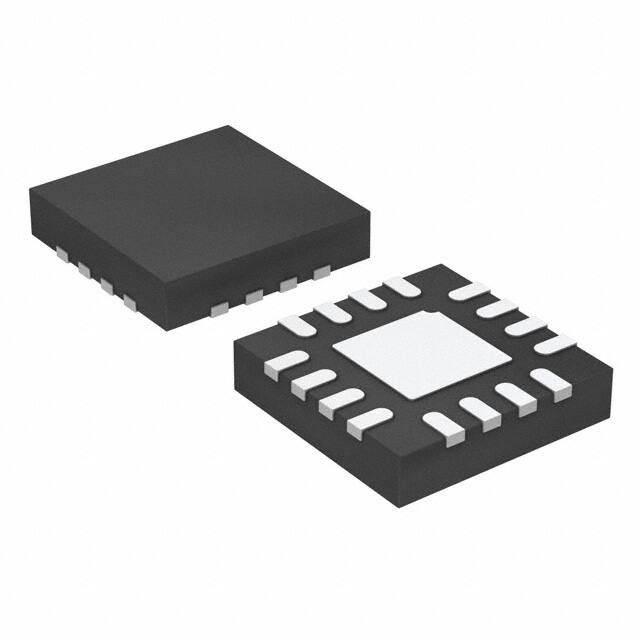
– 16 HTSSOP (PowerPAD™) 5.00 × 6.40 mm
– 16 QFN (PowerPAD) 3.00 × 3.00 mm
Protection Features
– VM Undervoltage Lockout (UVLO)
– Overcurrent Protection (OCP)
– Thermal Shutdown (TSD)
– Fault Indication Pin (nFAULT)
Point-of-Sale Printers
Video Security Cameras
Office Automation Machines
Gaming Machines
Robotics
Battery-Powered Toys
3 Description
The DRV8833C provides a dual-bridge motor driver
solution for toys, printers, and other mechatronic
applications.
The device has two H-bridges and can drive two DC
brushed motors, a bipolar stepper motor, solenoids,
or other inductive loads.
Each H-bridge output consists of a pair of N-channel
and P-channel MOSFETs, with circuitry that regulates
the winding current. With proper PCB design, each Hbridge of the DRV8833C can drive up to 700-mA
RMS (or DC) continuously, at 25°C with a VM supply
of 5 V. The device can support peak currents of up to
1 A per bridge. Current capability is reduced slightly
at lower VM voltages.
Internal shutdown functions with a fault output pin are
provided for overcurrent protection, short-circuit
protection, UVLO, and overtemperature. A low-power
sleep mode is also provided.
Device Information(1)
PART NUMBER
DRV8833C
PACKAGE
BODY SIZE (NOM)
HTSSOP (16)
5.00 mm × 6.40 mm
QFN (16)
3.00 mm × 3.00 mm
(1) For all available packages, see the orderable addendum at
the end of the data sheet.
2.7 to 10.8 V
M
0.7 A
nSLEEP
nFAULT
t
Controller
DRV8833C
+
PWM
Stepper or
Brushed DC
Motor Driver
+
t
0.7 A
1
An IMPORTANT NOTICE at the end of this data sheet addresses availability, warranty, changes, use in safety-critical applications,
intellectual property matters and other important disclaimers. PRODUCTION DATA.
�DRV8833C
SLVSCP9 – AUGUST 2014
www.ti.com
Table of Contents
1
2
3
4
5
6
7
Features ..................................................................
Applications ...........................................................
Description .............................................................
Revision History.....................................................
Pin Configuration and Functions .........................
Specifications.........................................................
1
1
1
2
3
4
6.1
6.2
6.3
6.4
6.5
6.6
4
4
4
5
5
7
Absolute Maximum Ratings ......................................
Handling Ratings.......................................................
Recommended Operating Conditions.......................
Thermal Information ..................................................
Electrical Characteristics...........................................
Typical Characteristics ..............................................
7.3 Feature Description................................................... 9
7.4 Device Functional Modes........................................ 13
8
Application and Implementation ........................ 14
8.1 Application Information............................................ 14
8.2 Typical Application ................................................. 14
9
Power Supply Recommendations...................... 17
9.1 Sizing Bulk Capacitance for Motor Drive Systems . 17
10 Layout................................................................... 18
10.1 Layout Guidelines ................................................. 18
10.2 Layout Example .................................................... 18
11 Device and Documentation Support ................. 19
11.1 Trademarks ........................................................... 19
11.2 Electrostatic Discharge Caution ............................ 19
11.3 Glossary ................................................................ 19
Detailed Description .............................................. 8
7.1 Overview ................................................................... 8
7.2 Functional Block Diagram ......................................... 8
12 Mechanical, Packaging, and Orderable
Information ........................................................... 19
4 Revision History
2
DATE
REVISION
NOTES
August 2014
*
Initial release.
Submit Documentation Feedback
Copyright © 2014, Texas Instruments Incorporated
Product Folder Links: DRV8833C
�DRV8833C
www.ti.com
SLVSCP9 – AUGUST 2014
5 Pin Configuration and Functions
HTSSOP (PWP)
16 Pins
Top View
10
8
9
AISEN
AOUT2
BOUT2
BISEN
13
1
12
2
11
GND
(PPAD)
3
10
4
9
VINT
GND
VM
NC
8
11
7
14
12
6
7
5
nFAULT
BIN1
BIN2
13
GND
(PPAD)
AOUT1
nSLEEP
AIN1
AIN2
14
4
15
3
AIN1
AIN2
VINT
GND
VM
NC
BIN2
BIN1
16
15
6
16
2
5
1
BOUT1
nSLEEP
AOUT1
AISEN
AOUT2
BOUT2
BISEN
BOUT1
nFAULT
QFN (RTE)
16 Pins
Top View
Pin Functions
PIN
NAME
PWP
RTE
TYPE
DESCRIPTION
POWER AND GROUND
GND
13
11
PWR
VINT
14
12
—
Device ground
Both the GND pin and device PowerPAD must be connected to ground
Internal regulator (3.3 V)
Internal supply voltage; bypass to GND with 2.2-μF, 6.3-V capacitor
VM
12
10
PWR
Power supply
Connect to motor supply voltage; bypass to GND with a 10-µF
(minimum) capacitor rated for VM
AIN1
16
14
AIN2
15
13
I
H-bridge A PWM input
Controls the state of AOUT1 and AOUT2; internal pulldown
BIN1
9
7
BIN2
10
8
I
H-bridge B PWM input
Controls the state of BOUT1 and BOUT2; internal pulldown
nSLEEP
1
15
I
Sleep mode input
Logic high to enable device; logic low to enter low-power sleep mode;
internal pulldown
8
6
OD
Fault indication pin
Pulled logic low with fault condition; open-drain output requires an
external pullup
AISEN
3
1
O
Bridge A sense
Sense resistor to GND sets PWM current regulation level (see PWM
Motor Drivers)
AOUT1
2
16
AOUT2
4
2
O
Bridge A output
Positive current is AOUT1 → AOUT2
BISEN
6
4
O
Bridge B sense
Sense resistor to GND sets PWM current regulation level (see PWM
Motor Drivers)
BOUT1
7
5
BOUT2
5
3
O
Bridge B output
Positive current is BOUT1 → BOUT2
CONTROL
STATUS
nFAULT
OUTPUT
Submit Documentation Feedback
Copyright © 2014, Texas Instruments Incorporated
Product Folder Links: DRV8833C
3
�DRV8833C
SLVSCP9 – AUGUST 2014
www.ti.com
External Components
Component
(1)
(2)
Pin 1
Pin 2
Recommended
(1)
CVM
VM
GND
10-µF
CVINT
VINT
GND
6.3-V, 2.2-µF ceramic capacitor
ceramic capacitor rated for VM
RnFAULT
VINT (2)
nFAULT
RAISEN
AISEN
GND
Sense resistor, see Typical Application for sizing
RBISEN
BISEN
GND
Sense resistor, see Typical Application for sizing
>1 kΩ
Proper bulk capacitance sizing depends on the motor power.
nFAULT may be pulled up to an external supply rated < 5.5 V.
6 Specifications
6.1 Absolute Maximum Ratings
over operating free-air temperature (unless otherwise noted)
Voltage
(1)
MIN
MAX
UNIT
Power supply (VM)
–0.3
11.8
V
Internal regulator (VINT)
–0.3
3.8
V
Control pins (AIN1, AIN2, BIN1, BIN2, nSLEEP, nFAULT)
–0.3
7
V
Continuous phase node pins (AOUT1, AOUT2, BOUT1, BOUT2)
–0.3
VM + 0.5
V
–1
VM + 1
V
–0.3
0.5
V
–1
1
V
Peak drive current (AOUT1, AOUT2, BOUT1, BOUT2, AISEN, BISEN)
Internally limited
A
Operating junction temperature
–40
°C
Pulsed 10 µs phase node pins (AOUT1, AOUT2, BOUT1, BOUT2)
Continuous shunt amplifier input pins (AISEN, BISEN)
Pulsed 10 µs shunt amplifier input pins (AISEN, BISEN)
TJ
(1)
150
Stresses beyond those listed under Absolute Maximum Ratings may cause permanent damage to the device. These are stress ratings
only, which do not imply functional operation of the device at these or any other conditions beyond those indicated under Recommended
Operating Conditions. Exposure to absolute-maximum-rated conditions for extended periods may affect device reliability.
6.2 Handling Ratings
MIN
Tstg
Storage temperature range
V(ESD)
Electrostatic
discharge
(1)
(2)
MAX
UNIT
°C
–65
150
Human body model (HBM), per ANSI/ESDA/JEDEC JS-001, all pins (1)
–2000
2000
Charged device model (CDM), per JEDEC specification JESD22-C101, all pins (2)
–1000
1000
V
JEDEC document JEP155 states that 500-V HBM allows safe manufacturing with a standard ESD control process.
JEDEC document JEP157 states that 250-V CDM allows safe manufacturing with a standard ESD control process.
6.3 Recommended Operating Conditions
over operating free-air temperature range (unless otherwise noted)
VM
Power supply voltage range
VI
Logic level input voltage
MIN
MAX
UNIT
2.7
10.8
V
0
5.5
V
PWP package
0
0.7
A
RTE package
0
0.6
A
0
200
kHz
–40
85
°C
(1)
IRMS
Motor RMS current (2)
ƒPWM
Applied PWM signal to AIN1, AIN2, BIN1, or BIN2
TA
Operating ambient temperature
(1)
(2)
4
Note that when VM is below 5 V, RDS(ON) increases and maximum output current is reduced.
Power dissipation and thermal limits must be observed.
Submit Documentation Feedback
Copyright © 2014, Texas Instruments Incorporated
Product Folder Links: DRV8833C
�DRV8833C
www.ti.com
SLVSCP9 – AUGUST 2014
6.4 Thermal Information
DRV8833C
THERMAL METRIC (1)
HTSSOP
QFN
16 PINS
16 PINS
RθJA
Junction-to-ambient thermal resistance
40.5
44.7
RθJC(top)
Junction-to-case (top) thermal resistance
32.9
48.5
RθJB
Junction-to-board thermal resistance
28.8
16.8
ψJT
Junction-to-top characterization parameter
0.6
0.7
ψJB
Junction-to-board characterization parameter
11.5
16.7
RθJC(bot)
Junction-to-case (bottom) thermal resistance
4.8
4.2
(1)
UNIT
°C/W
For more information about traditional and new thermal metrics, see the IC Package Thermal Metrics application report, SPRA953.
6.5 Electrical Characteristics
over operating free-air temperature range (unless otherwise noted)
PARAMETER
TEST CONDITIONS
MIN
TYP
MAX
UNIT
10.8
V
POWER SUPPLIES (VM, VINT)
VM
VM operating voltage
2.7
IVM
VM operating supply current
VM = 5 V, xINx low, nSLEEP high
1.7
3
mA
IVMQ
VM sleep mode supply current
VM = 5 V, nSLEEP low
1.6
2.7
μA
tSLEEP
Sleep time
nSLEEP low to sleep mode
10
µs
tWAKE
Wake-up time
nSLEEP high to output transition
155
μs
tON
Turn-on time
VM > VUVLO to output transition
VINT
Internal regulator voltage
VM = 5 V
μs
25
3
3.3
3.6
V
CONTROL INPUTS (AIN1, AIN2, BIN1, BIN2, nSLEEP)
xINx
0
0.7
nSLEEP
0
0.5
xINx
2
5.5
2.5
5.5
VIL
Input logic low voltage
VIH
Input logic high voltage
VHYS
Input logic hysteresis
IIL
Input logic low current
VIN = 0 V
IIH
Input logic high current
VIN = 5 V
RPD
Pulldown resistance
tDEG
Input deglitch time
tPROP
Propagation delay INx to OUTx
nSLEEP
350
400
–1
V
650
mV
1
μA
50
μA
xINx
100
150
250
nSLEEP
380
500
750
VM = 5 V
V
kΩ
575
ns
1.2
μs
CONTROL OUTPUTS (nFAULT)
VOL
Output logic low voltage
IO = 5 mA
IOH
Output logic high leakage
RPULLUP = 1 kΩ to 5 V
–1
0.5
V
1
μA
MOTOR DRIVER OUTPUTS (AOUT1, AOUT2, BOUT1, BOUT2)
VM = 5 V, I = 0.2 A, TA = 25°C
RDS(ON)
RDS(ON)
(1)
High-side FET on-resistance
Low-side FET on-resistance
1180
(1)
1400
VM = 2.7 V, I = 0.2 A, TA = 25°C
1550
VM = 2.7 V, I = 0.2 A, TA = 85°C (1)
1875
VM = 5 V, I = 0.2 A, TA = 85°C
VM = 5 V, I = 0.2 A, TA = 25°C
555
VM = 5 V, I = 0.2 A, TA = 85°C (1)
675
VM = 2.7 V, I = 0.2 A, TA = 25°C
635
VM = 2.7 V, I = 0.2 A, TA = 85°C (1)
775
1475
mΩ
1975
705
mΩ
815
Not tested in production; based on design and characterization data
Submit Documentation Feedback
Copyright © 2014, Texas Instruments Incorporated
Product Folder Links: DRV8833C
5
�DRV8833C
SLVSCP9 – AUGUST 2014
www.ti.com
Electrical Characteristics (continued)
over operating free-air temperature range (unless otherwise noted)
PARAMETER
TEST CONDITIONS
MIN
TYP
–1
MAX
1
UNIT
μA
IOFF
Off-state leakage current
VM = 5 V
tRISE
Output rise time
VM = 5 V; RL = 16 Ω to GND
70
ns
tFALL
Output fall time
VM = 5 V; RL = 16 Ω to VM
80
ns
tDEAD
Output dead time
Internal dead time
450
ns
PWM CURRENT CONTROL (AISEN, BISEN)
VTRIP
xISEN trip voltage
tOFF
Current control constant off time
160
Internal PWM constant off time
200
240
20
mV
µs
PROTECTION CIRCUITS
VM falling; UVLO report
2.6
VM rising; UVLO recovery
2.7
VUVLO
VM undervoltage lockout
VUVLO,HYS
VM undervoltage hysteresis
IOCP
Overcurrent protection trip level
tDEG
Overcurrent deglitch time
tOCP
Overcurrent protection period
TTSD (2)
Thermal shutdown temperature
Die temperature, TJ
THYS
Thermal shutdown hysteresis
Die temperature, TJ
(2)
6
Rising to falling threshold
V
90
mV
2.3
μs
1.4
ms
1
A
150
°C
20
°C
Not tested in production; based on design and characterization data
Submit Documentation Feedback
Copyright © 2014, Texas Instruments Incorporated
Product Folder Links: DRV8833C
�DRV8833C
www.ti.com
SLVSCP9 – AUGUST 2014
6.6 Typical Characteristics
1.8
25
TA� �±��&
TA = 25°C
TA = 85°C
20
IVMQ (PA)
1.6
IVM (mA)
TA� �±��&
TA = 25°C
TA = 85°C
1.4
15
10
1.2
5
1
0
2
4
6
8
10
12
VM (V)
2
4
6
8
10
VM (V)
D001
Figure 1. Supply Current
D002
Figure 2. Sleep Current
1
2.5
TA� �±��&
TA = 25°C
TA = 85°C
TA� �±��&
TA = 25°C
TA = 85°C
2
Low-Side RDS(ON) (:)
High-Side RDS(ON) (:)
12
1.5
1
0.75
0.5
0.25
0.5
2
4
6
8
10
2
12
VM (V)
4
6
8
10
VM (V)
D004
Figure 3. High-Side RDS(ON)
12
D005
Figure 4. Low-Side RDS(ON)
4
VINT (V)
3.5
3
2.5
2
2
4
6
8
VM (V)
10
12
D003
Figure 5. VINT Over VM
Submit Documentation Feedback
Copyright © 2014, Texas Instruments Incorporated
Product Folder Links: DRV8833C
7
�DRV8833C
SLVSCP9 – AUGUST 2014
www.ti.com
7 Detailed Description
7.1 Overview
The DRV8833C device is an integrated motor driver solution for brushed DC or bipolar stepper motors. The
device integrates two PMOS + NMOS H-bridges and current regulation circuitry. The DRV8833C can be
powered with a supply voltage from 2.7 to 10.8 V and can provide an output current up to 700 mA RMS.
A simple PWM interface allows easy interfacing to the controller circuit.
The current regulation is a 20-µs fixed off-time slow decay.
The device includes a low-power sleep mode, which lets the system save power when not driving the motor.
7.2 Functional Block Diagram
VM
VM
10 µF
Internal
Reference and
Regulators
VINT
2.2 µF
VM
AOUT1
Gate
Drive
and
OCP
AIN1
AIN2
BDC
VM
Step
Motor
AOUT2
BIN1
BIN2
AISEN
ISEN
Logic
VM
BOUT1
Gate
Drive
and
OCP
nSLEEP
nFAULT
BDC
VM
BOUT2
OverTemp
ISEN
BISEN
GND
8
Submit Documentation Feedback
Copyright © 2014, Texas Instruments Incorporated
Product Folder Links: DRV8833C
�DRV8833C
www.ti.com
SLVSCP9 – AUGUST 2014
7.3 Feature Description
7.3.1 PWM Motor Drivers
The DRV8833C contains drivers for two full H-bridges. Figure 6 shows a block diagram of the circuitry.
VM
OCP
VM
xOUT1
xIN1
PreDrive
BDC
xOUT2
xIN2
PWM
OCP
xISEN
±
+
Optional
REF (200 mV)
Figure 6. H-Bridge and Current-Chopping Circuitry
7.3.2 Bridge Control and Decay Modes
The AIN1 and AIN2 input pins control the state of the AOUT1 and AOUT2 outputs; similarly, the BIN1 and BIN2
input pins control the state of the BOUT1 and BOUT2 outputs (see Table 1).
Table 1. H-Bridge Logic
xIN1
xIN2
xOUT1
xOUT2
FUNCTION
0
0
Z
Z
Coast / fast decay
0
1
L
H
Reverse
1
0
H
L
Forward
1
1
L
L
Brake / slow decay
The inputs can also be used for PWM control of the motor speed. When controlling a winding with PWM and the
drive current is interrupted, the inductive nature of the motor requires that the current must continue to flow
(called recirculation current). To handle this recirculation current, the H-bridge can operate in two different states,
fast decay or slow decay. In fast-decay mode, the H-bridge is disabled and recirculation current flows through the
body diodes. In slow-decay mode, the motor winding is shorted by enabling both low-side FETs.
To externally pulse-width modulate the bridge in fast-decay mode, the PWM signal is applied to one xIN pin while
the other is held low; to use slow-decay mode, one xIN pin is held high. See Table 2 for more information.
Submit Documentation Feedback
Copyright © 2014, Texas Instruments Incorporated
Product Folder Links: DRV8833C
9
�DRV8833C
SLVSCP9 – AUGUST 2014
www.ti.com
Table 2. PWM Control of Motor Speed
xIN1
xIN2
PWM
0
Forward PWM, fast decay
FUNCTION
1
PWM
Forward PWM, slow decay
0
PWM
Reverse PWM, fast decay
PWM
1
Reverse PWM, slow decay
The internal current control is still enabled when applying external PWM to xIN. To disable the current control
when applying external PWM, the xISEN pins should be connected directly to ground. Figure 7 show the current
paths in different drive and decay modes.
VM
VM
1 Forward drive
1
xOUT2
xOUT1
1 Reverse drive
1
2 Fast decay
3 Slow decay
xOUT2
xOUT1
2
2
3
3
FORWARD
2
Fast decay
3
Slow decay
REVERSE
Figure 7. Drive and Decay Modes
7.3.3 Current Control
The current through the motor windings may be limited, or controlled, by a 20-µs constant off-time PWM current
regulation, or current chopping. For DC motors, current control is used to limit the start-up and stall current of the
motor. For stepper motors, current control is often used at all times.
When an H-bridge is enabled, current rises through the winding at a rate dependent on the DC voltage and
inductance of the winding. If the current reaches the current chopping threshold, the bridge disables the current
until the beginning of the next PWM cycle. Note that immediately after the output is enabled, the voltage on the
xISEN pin is ignored for a fixed period of time before enabling the current sense circuitry. This blanking time is
fixed at 3.75 μs.
The PWM chopping current is set by a comparator that compares the voltage across a current sense resistor
connected to the xISEN pins with a reference voltage. The reference voltage, VTRIP, is is fixed at 200 mV
nominally.
The chopping current is calculated as in Equation 1.
200 mV
ICHOP
R XISEN
(1)
Example: If a 1-Ω sense resistor is used, the chopping current will be 200 mV / 1 Ω = 200 mA.
10
Submit Documentation Feedback
Copyright © 2014, Texas Instruments Incorporated
Product Folder Links: DRV8833C
�DRV8833C
www.ti.com
SLVSCP9 – AUGUST 2014
NOTE
If current control is not needed, the xISEN pins should be connected directly to ground.
7.3.4 Decay Mode
After the chopping current threshold is reached, the H-bridge switches to slow-decay mode. This state is held for
toff (20 µs) until the next cycle to turn on the high-side MOSFETs.
7.3.5 Slow Decay
xOUT1
xIN2
xIN1
In slow-decay mode, the high-side MOSFETs are turned off and both of the low-side MOSFETs are turned on.
The motor current decreases while flowing in the two low-side MOSFETs until reaching its fixed off time (typically
20 µs). After that, the high-side MOSFETs are enabled to increase the winding current again.
Drive Current (A)
ICHOP
Drive
Brake / Slow Decay
Drive
Brake / Slow Decay
tDRIVE
tOFF
tDRIVE
tOFF
Figure 8. Current Chopping Operation
7.3.6 Sleep Mode
Driving nSLEEP low puts the device into a low-power sleep state. In this state, the H-bridges are disabled, all
internal logic is reset, and all internal clocks are stopped. All inputs are ignored until nSLEEP returns inactive
high. When returning from sleep mode, some time, tWAKE, needs to pass before the motor driver becomes fully
operational. To make the board design simple, the nSLEEP can be pulled up to the supply (VM). TI recommends
to use a pullup resistor when this is done. This resistor limits the current to the input in case VM is higher than 6.5
V. Internally, the nSLEEP pin has a 500-kΩ resistor to GND. It also has a clamping Zener diode that clamps the
voltage at the pin at 6.5 V. Currents greater than 250 µA can cause damage to the input structure. Therefore, TI
recommends a pullup resistor between 20 to 75 kΩ.
Submit Documentation Feedback
Copyright © 2014, Texas Instruments Incorporated
Product Folder Links: DRV8833C
11
�DRV8833C
SLVSCP9 – AUGUST 2014
www.ti.com
7.3.7 Parallel Mode
The two H-bridges in the DRV8833C can be connected in parallel for double the current of a single H-bridge. The
internal dead time in the DRV8833C prevents any risk of cross-conduction (shoot-through) between the two
bridges due to timing differences between the two bridges. Figure 9 shows the connections.
VM
+
nSLEEP
nFAULT
NC
11
2
AOUT1
4
AOUT2
7
BOUT1
5
BOUT2
3
AISEN
6
BISEN
BDC
13
2.2 µF
PPAD
GND
16
AIN1
15
AIN2
9
BIN1
10
BIN2
1
nSLEEP
8
nFAULT
14
VINT
IN1
IN2
VM
12
10 µF
Figure 9. Parallel Mode Schematic
7.3.8 Protection Circuits
The DRV8833C is fully protected against overcurrent, overtemperature, and undervoltage events.
7.3.8.1 Overcurrent Protection (OCP)
An analog current limit (IOCP) circuit on each FET limits the current through the FET by limiting the gate drive. If
this analog current limit persists for longer than the OCP deglitch time (tDEG), all FETs in the H-bridge are
disabled and the nFAULT pin is driven low. The driver is re-enabled after the OCP retry period (tOCP) has passed.
nFAULT becomes high again after the retry time. If the fault condition is still present, the cycle repeats. If the
fault is no longer present, normal operation resumes and nFAULT remains deasserted. Note that only the Hbridge in which the OCP is detected will be disabled while the other bridge functions normally.
Overcurrent conditions are detected independently on both high-side and low-side devices; a short to ground,
supply, or across the motor winding all result in an overcurrent shutdown. Note that overcurrent protection does
not use the current sense circuitry used for PWM current control, so it functions even without presence of the
xISEN resistors.
7.3.8.2 Thermal Shutdown (TSD)
If the die temperature exceeds safe limits, all FETs in the H-bridge are disabled and the nFAULT pin is driven
low. After the die temperature has fallen below the specified hysteresis (THYS), operation automatically resumes.
The nFAULT pin is released after operation has resumed.
7.3.8.3 UVLO
If at any time the voltage on the VM pin falls below the UVLO threshold voltage, VUVLO, all circuitry in the device is
disabled, and all internal logic is reset. Operation resumes when VM rises above the UVLO threshold. The
nFAULT pin is not driven low during an undervoltage condition.
12
Submit Documentation Feedback
Copyright © 2014, Texas Instruments Incorporated
Product Folder Links: DRV8833C
�DRV8833C
www.ti.com
SLVSCP9 – AUGUST 2014
Table 3. Device Protection
Condition
Error Report
H-Bridge
Internal Circuits
Recovery
VM undervoltage (UVLO)
Fault
VM < 2.6 V
None
Disabled
Disabled
VM > 2.7 V
Overcurrent (OCP)
IOUT > IOCP
FAULTn
Disabled
Operating
OCP
TJ > TTSD
FAULTn
Disabled
Operating
TJ < TTSD – THYS
Thermal Shutdown (TSD)
7.4 Device Functional Modes
The DRV8833C is active unless the nSLEEP pin is brought logic low. In sleep mode, the H-bridge FETs are
disabled (Hi-Z). Note that tSLEEP must elapse after a falling edge on the nSLEEP pin before the device is in sleep
mode. The DRV8833C is brought out of sleep mode automatically if nSLEEP is brought logic high. Note that
tWAKE must elapse before the outputs change state after wake-up.
Table 4. Modes of Operation
Fault
Condition
H-Bridge
Internal Circuits
Operating
nSLEEP pin high
Operating
Operating
Sleep mode
nSLEEP pin low
Disabled
Disabled
Any fault condition met
Disabled
See Table 3
Fault encountered
Submit Documentation Feedback
Copyright © 2014, Texas Instruments Incorporated
Product Folder Links: DRV8833C
13
�DRV8833C
SLVSCP9 – AUGUST 2014
www.ti.com
8 Application and Implementation
8.1 Application Information
The DRV8833C is used in stepper or brushed DC motor control. The following design procedure can be used to
configure the DRV8833C in a bipolar stepper motor application.
8.2 Typical Application
DRV8833CPWP
1
3
1
4
±
Step
Motor
+
2
+
5
±
6
1
7
8
nSLEEP
AIN1
AOUT1
AIN2
AISEN
VINT
AOUT2
GND
BOUT2
VM
BISEN
NC
BOUT1
BIN2
nFAULT
BIN1
16
15
14
13
2.2 µF
12
10 µF
11
VM
10
9
10 k
VCC, logic supply
8.2.1 Design Requirements
Table 5 gives design input parameters for system design.
Table 5. Design Parameters
Design Parameter
Reference
Example Value
Supply voltage
VM
9V
Motor winding resistance
RL
12 Ω/phase
Motor winding inductance
LL
10 mH/phase
Motor full step angle
θstep
1.8 °/step
Target stepping level
nm
2 (half-stepping)
Target motor speed
v
120 rpm
Target chopping current
ICHOP
200 mA
Sense resistor
RISEN
1Ω
8.2.2 Detailed Design Procedure
8.2.2.1 Stepper Motor Speed
The first step in configuring the DRV8833C requires the desired motor speed and stepping level. The DRV8833C
can support full- and half-stepping modes using the PWM interface.
If the target motor speed is too high, the motor does not spin. Ensure that the motor can support the target
speed.
For a desired motor speed (v), microstepping level (nm), and motor full step angle (θstep),
¦step �VWHSV � V�
14
v(rpm) u nm � steps � u 360q / rot
Tstep � q / step � u 60 s / min
Submit Documentation Feedback
(2)
Copyright © 2014, Texas Instruments Incorporated
Product Folder Links: DRV8833C
�DRV8833C
www.ti.com
SLVSCP9 – AUGUST 2014
AIN1
AIN2
BIN1
BIN2
Forward
IAOUT
Reverse
Forward
Forward
IBOUT
Reverse
Figure 10. Full-Step Mode
AIN1
AIN2
BIN1
BIN2
Forward
IAOUT
Reverse
Forward
Forward
IBOUT
Reverse
Figure 11. Half-Step Mode
8.2.2.2 Current Regulation
The chopping current (ICHOP) is the maximum current driven through either winding. This quantity depends on the
sense resistor value (RXISEN).
200 mV
ICHOP
R XISEN
(3)
Submit Documentation Feedback
Copyright © 2014, Texas Instruments Incorporated
Product Folder Links: DRV8833C
15
�DRV8833C
SLVSCP9 – AUGUST 2014
www.ti.com
ICHOP is set by a comparator which compares the voltage across RXISEN to a reference voltage. Note that ICHOP
must follow Equation 4 to avoid saturating the motor.
VM (V)
IFS (A) �
RL (:) � RDS(ON) HS (:) � RDS(ON) LS (:)
where
•
•
VM is the motor supply voltage.
RL is the motor winding resistance.
(4)
8.2.3 Application Curve
A.
Channel 1 is the AIN1 input PWM signal, and channel 2 is the AIN2 input PWM signal. BIN1 and BIN2 follow the
same pattern, but are shifted by 90° from AIN1 and AIN2 as shown in Figure 11. Channel 4 is the output current in
the direction AOUT1 → AOUT2. In forward and reverse drive, the current rises until it hits the current chopping limit of
200 mA, and is regulated at that level with fixed-off time current chopping.
Figure 12. ½ Stepping Operation
16
Submit Documentation Feedback
Copyright © 2014, Texas Instruments Incorporated
Product Folder Links: DRV8833C
�DRV8833C
www.ti.com
SLVSCP9 – AUGUST 2014
9 Power Supply Recommendations
The DRV8833C is designed to operate from an input voltage supply (VM) range between 2.7 to 10.8 V. A 10-µF
ceramic capacitor rated for VM must be placed as close to the DRV8833C as possible.
9.1 Sizing Bulk Capacitance for Motor Drive Systems
Bulk capacitance sizing is an important factor in motor drive system design. It depends on a variety of factors
including:
• Type of power supply
• Acceptable supply voltage ripple
• Parasitic inductance in the power supply wiring
• Type of motor (brushed DC, brushless DC, stepper)
• Motor startup current
• Motor braking method
The inductance between the power supply and motor drive system limits the rate current can change from the
power supply. If the local bulk capacitance is too small, the system responds to excessive current demands or
dumps from the motor with a change in voltage. Size the bulk capacitance to meet acceptable voltage ripple
levels.
The data sheet generally provides a recommended value, but system-level testing is required to determine the
appropriate-sized bulk capacitor.
Parasitic Wire
Inductance
Motor Drive System
Power Supply
VM
+
Motor Driver
t
GND
Bypass/Bulk
Capacitor
Power Supply
Inductance
Figure 13. Setup of Motor Drive System With External Power Supply
Submit Documentation Feedback
Copyright © 2014, Texas Instruments Incorporated
Product Folder Links: DRV8833C
17
�DRV8833C
SLVSCP9 – AUGUST 2014
www.ti.com
10 Layout
10.1 Layout Guidelines
Bypass the VM terminal to GND using a low-ESR ceramic bypass capacitor with a recommended value of 10 µF
rated for VM. This capacitor should be placed as close to the VM pin as possible with a thick trace or ground
plane connection to the device GND pin and PowerPAD.
Bypass VINT to ground with a ceramic capacitor rated 6.3 V. Place this bypassing capacitor as close to the pin
as possible.
10.2 Layout Example
nSLEEP
AIN1
AOUT1
AIN2
2.2 µF
RAISEN
RBISEN
18
AISEN
VINT
AOUT2
GND
BOUT2
VM
BISEN
NC
BOUT1
BIN2
nFAULT
BIN1
Submit Documentation Feedback
10 µF
Copyright © 2014, Texas Instruments Incorporated
Product Folder Links: DRV8833C
�DRV8833C
www.ti.com
SLVSCP9 – AUGUST 2014
11 Device and Documentation Support
11.1 Trademarks
PowerPAD is a trademark of Texas Instruments.
11.2 Electrostatic Discharge Caution
These devices have limited built-in ESD protection. The leads should be shorted together or the device placed in conductive foam
during storage or handling to prevent electrostatic damage to the MOS gates.
11.3 Glossary
SLYZ022 — TI Glossary.
This glossary lists and explains terms, acronyms, and definitions.
12 Mechanical, Packaging, and Orderable Information
The following pages include mechanical, packaging, and orderable information. This information is the most
current data available for the designated devices. This data is subject to change without notice and revision of
this document. For browser-based versions of this data sheet, refer to the left-hand navigation.
Submit Documentation Feedback
Copyright © 2014, Texas Instruments Incorporated
Product Folder Links: DRV8833C
19
�PACKAGE OPTION ADDENDUM
www.ti.com
11-Aug-2022
PACKAGING INFORMATION
Orderable Device
Status
(1)
Package Type Package Pins Package
Drawing
Qty
Eco Plan
(2)
Lead finish/
Ball material
MSL Peak Temp
Op Temp (°C)
Device Marking
(3)
Samples
(4/5)
(6)
DRV8833CPWP
ACTIVE
HTSSOP
PWP
16
90
RoHS & Green
NIPDAU
Level-3-260C-168 HR
-40 to 85
8833C
Samples
DRV8833CPWPR
ACTIVE
HTSSOP
PWP
16
2000
RoHS & Green
NIPDAU
Level-3-260C-168 HR
-40 to 85
8833C
Samples
DRV8833CRTER
ACTIVE
WQFN
RTE
16
3000
RoHS & Green
NIPDAU
Level-1-260C-UNLIM
-40 to 85
8833C
Samples
DRV8833CRTET
ACTIVE
WQFN
RTE
16
250
RoHS & Green
NIPDAU
Level-1-260C-UNLIM
-40 to 85
8833C
Samples
(1)
The marketing status values are defined as follows:
ACTIVE: Product device recommended for new designs.
LIFEBUY: TI has announced that the device will be discontinued, and a lifetime-buy period is in effect.
NRND: Not recommended for new designs. Device is in production to support existing customers, but TI does not recommend using this part in a new design.
PREVIEW: Device has been announced but is not in production. Samples may or may not be available.
OBSOLETE: TI has discontinued the production of the device.
(2)
RoHS: TI defines "RoHS" to mean semiconductor products that are compliant with the current EU RoHS requirements for all 10 RoHS substances, including the requirement that RoHS substance
do not exceed 0.1% by weight in homogeneous materials. Where designed to be soldered at high temperatures, "RoHS" products are suitable for use in specified lead-free processes. TI may
reference these types of products as "Pb-Free".
RoHS Exempt: TI defines "RoHS Exempt" to mean products that contain lead but are compliant with EU RoHS pursuant to a specific EU RoHS exemption.
Green: TI defines "Green" to mean the content of Chlorine (Cl) and Bromine (Br) based flame retardants meet JS709B low halogen requirements of


 工商网监
湘ICP备2023018690号
工商网监
湘ICP备2023018690号
