DRV8837, DRV8838
DRV8837,
SLVSBA4F – JUNE 2012
– REVISED DRV8838
APRIL 2021
SLVSBA4F – JUNE 2012 – REVISED APRIL 2021
www.ti.com
DRV883x Low-Voltage H-Bridge Driver
1 Features
3 Description
•
The DRV883x family of devices provides an
integrated motor driver solution for cameras,
consumer products, toys, and other low-voltage or
battery-powered motion control applications. The
device can drive one dc motor or other devices
like solenoids. The output driver block consists of Nchannel power MOSFETs configured as an H-bridge
to drive the motor winding. An internal charge pump
generates needed gate drive voltages.
•
•
•
•
•
•
H-Bridge Motor Driver
– Drives a DC Motor or Other Loads
– Low MOSFET On-Resistance: HS + LS
280 mΩ
1.8-A Maximum Drive Current
Separate Motor and Logic Supply Pins:
– Motor VM: 0 to 11 V
– Logic VCC: 1.8 to 7 V
PWM or PH-EN Interface
– DRV8837: PWM, IN1 and IN2
– DRV8838: PH and EN
Low-Power Sleep Mode With 120-nA Maximum
Sleep Current
– nSLEEP pin
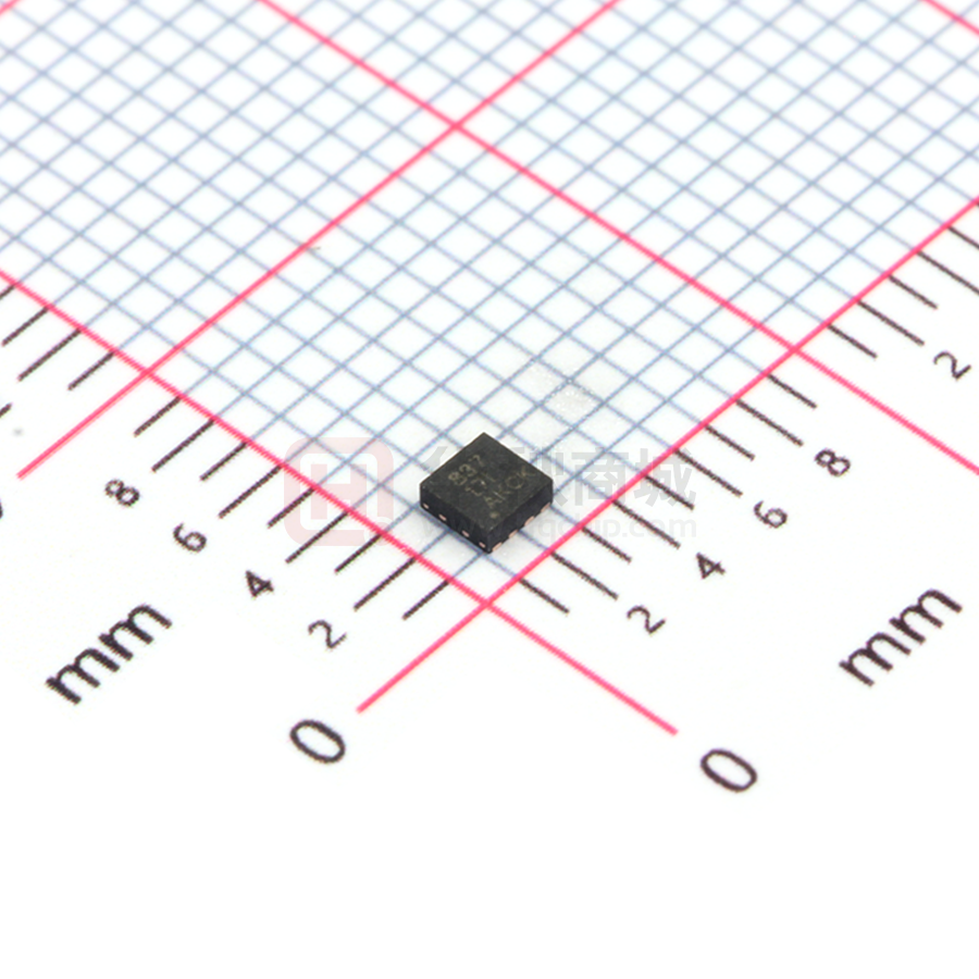
Small Package and Footprint
– 8-Pin WSON With Thermal Pad
– 2.0 × 2.0 mm
Protection Features
– VCC Undervoltage Lockout (UVLO)
– Overcurrent Protection (OCP)
– Thermal Shutdown (TSD)
The DRV883x family of devices can supply up to
1.8 A of output current. It operates on a motor power
supply voltage from 0 to 11 V, and a device power
supply voltage of 1.8 V to 7 V.
The DRV8837 device has a PWM (IN1-IN2) input
interface; the DRV8838 device has a PH-EN
input interface. Both interfaces are compatible with
industry-standard devices.
Internal shutdown functions are provided for
overcurrent protection, short-circuit protection,
undervoltage lockout, and overtemperature.
Device Information(1)
2 Applications
•
•
•
•
•
•
Cameras
DSLR Lenses
Consumer Products
Toys
Robotics
Medical Devices
PART NUMBER
DRV8837
WSON (8)
DRV8838
(1)
PACKAGE
BODY SIZE (NOM)
2.00 mm × 2.00 mm
For all available packages, see the orderable addendum at
the end of the data sheet.
1.8 V to 7 V
VCC
Controller
PWM
or
PH and EN
0 V to 11 V
VM
DRV8837 and
DRV8838
1.8 A
nSLEEP
M
Brushed DC Motor
Driver
DRV883x Simplified Diagram
An©IMPORTANT
NOTICEIncorporated
at the end of this data sheet addresses availability, warranty, changes, use in
safety-critical
applications,
Copyright
2021 Texas Instruments
Submit
Document
Feedback
intellectual property matters and other important disclaimers. PRODUCTION DATA.
1
�DRV8837, DRV8838
www.ti.com
SLVSBA4F – JUNE 2012 – REVISED APRIL 2021
Table of Contents
1 Features............................................................................1
2 Applications..................................................................... 1
3 Description.......................................................................1
4 Revision History.............................................................. 2
5 Pin Configuration and Functions...................................4
Pin Functions.................................................................... 4
5.1 Dapper Pin Functions................................................. 4
6 Specifications.................................................................. 6
6.1 Absolute Maximum Ratings........................................ 6
6.2 ESD Ratings............................................................... 6
6.3 Recommended Operating Conditions.........................6
6.4 Thermal Information....................................................6
6.5 Electrical Characteristics.............................................8
6.6 Timing Requirements.................................................. 9
6.7 Typical Characteristics.............................................. 10
7 Detailed Description...................................................... 11
7.1 Overview................................................................... 11
7.2 Functional Block Diagram......................................... 11
7.3 Feature Description...................................................13
7.4 Device Functional Modes..........................................16
8 Power Supply Recommendations................................19
8.1 Bulk Capacitance...................................................... 19
9 Layout.............................................................................20
9.1 Layout Guidelines..................................................... 20
9.2 Layout Example........................................................ 20
9.3 Power Dissipation..................................................... 20
10 Device and Documentation Support..........................21
10.1 Documentation Support.......................................... 21
10.2 Related Links.......................................................... 21
10.3 Receiving Notification of Documentation Updates..21
10.4 Community Resources............................................21
10.5 Trademarks............................................................. 21
4 Revision History
NOTE: Page numbers for previous revisions may differ from page numbers in the current version.
Changes from Revision E (June 2016) to Revision F (April 2021)
Page
• Updated the numbering format for tables, figures, and cross-references throughout the document..................1
• Added in the Independent Half-Bridge Control section.....................................................................................13
Changes from Revision D (December 2015) to Revision E (June 2016)
Page
• Changed the threshold type to the input logic voltage parameters in the Electrical Characteristics table..........8
• Changed the units for the input logic hysteresis parameter from mV to V in the Electrical Characteristics table
............................................................................................................................................................................8
• Added the Receiving Notification of Documentation Updates section .............................................................21
Changes from Revision C (February 2014) to Revision D (December 2015)
Page
• Clarified the input interface for each device in the Description section ............................................................. 1
• Added CDM and HBM ESD ratings to the ESD Ratings table ...........................................................................6
Changes from Revision B (December 2013) to Revision C (February 2014)
Page
• Added the DRV8838 device information, specifications, and timing diagrams...................................................1
• Added Device Information table..........................................................................................................................1
• Added a PWM interface diagram .......................................................................................................................1
• Added more information to the Detailed Description and moved information from the Functional Description ...
11
• Added functional block diagram for DRV8838 ................................................................................................. 11
• Added the Application and Implementation section .........................................................................................17
• Added Power Supply Recommendations, Layout, Device and Documentation Support, and Mechanical,
Packaging, and Orderable Information sections...............................................................................................19
2
Submit Document Feedback
Copyright © 2021 Texas Instruments Incorporated
�www.ti.com
DRV8837, DRV8838
SLVSBA4F – JUNE 2012 – REVISED APRIL 2021
Changes from Revision A (August 2012) to Revision B (December 2013)
Page
• Changed Features section..................................................................................................................................1
• Changed Recommended Operating Conditions................................................................................................. 6
• Changed Electrical Characteristics section........................................................................................................ 8
• Changed Timing Requirements section..............................................................................................................9
• Changed Power Supplies and Input Pins section.............................................................................................16
Copyright © 2021 Texas Instruments Incorporated
Submit Document Feedback
3
�DRV8837, DRV8838
www.ti.com
SLVSBA4F – JUNE 2012 – REVISED APRIL 2021
5 Pin Configuration and Functions
VM
1
OUT1
2
8
VCC
7
nSLEEP
VM
1
OUT1
2
Thermal
OUT2
3
GND
4
8
VCC
7
nSLEEP
6
PH
5
EN
Thermal
Pad
6
IN1
OUT2
3
5
IN2
GND
4
Figure 5-1. DSG Package 8-Pin WSON With
Thermal Pad DRV8837 Top View
Pad
Figure 5-2. DSG Package 8-Pin WSON With
Thermal Pad DRV8838 Top View
Pin Functions
PIN
NAME
NO.
DRV8837
I/O
DESCRIPTION
DRV8838
POWER AND GROUND
Device ground
This pin must be connected to ground.
GND
4
4
—
VCC
8
8
I
Logic power supply
Bypass this pin to the GND pin with a 0.1-µF ceramic capacitor rated for VCC.
VM
1
1
I
Motor power supply
Bypass this pin to the GND pin with a 0.1-µF ceramic capacitor rated for VM.
EN
—
5
I
ENABLE input
IN1
6
—
I
IN1 input
See the Section 7 section for more information.
IN2
5
—
I
IN2 input
See the Section 7 section for more information.
PH
—
6
I
PHASE input
See the Section 7 section for more information.
nSLEEP
7
7
I
Sleep mode input
When this pin is in logic low, the device enters low-power sleep mode. The device operates
normally when this pin is logic high. Internal pulldown
OUT1
2
2
O
OUT2
3
3
O
CONTROL
OUTPUT
Motor output
Connect these pins to the motor winding.
5.1 Dapper Pin Functions
PIN
DRV8837
NO.
DRV8838
NO.
I/O
GND
4
4
—
VCC
8
8
I
NAME
4
Submit Document Feedback
DESCRIPTION
Device ground
This pin must be connected to ground.
Logic power supply
Bypass this pin to the GND pin with a 0.1-µF ceramic capacitor rated for VCC.
Copyright © 2021 Texas Instruments Incorporated
�DRV8837, DRV8838
www.ti.com
SLVSBA4F – JUNE 2012 – REVISED APRIL 2021
PIN
DRV8837
NO.
DRV8838
NO.
I/O
VM
1
1
I
Motor power supply
Bypass this pin to the GND pin with a 0.1-µF ceramic capacitor rated for VM.
EN
—
5
I
ENABLE input
IN1
6
—
I
IN1 input
See the Section 7 section for more information.
IN2
5
—
I
IN2 input
See the Section 7 section for more information.
PH
—
6
I
PHASE input
See the Section 7 section for more information.
nSLEEP
7
7
I
Sleep mode input
When this pin is in logic low, the device enters low-power sleep mode. The device operates
normally when this pin is logic high. Internal pulldown
OUT1
2
2
O
OUT2
3
3
O
NAME
Copyright © 2021 Texas Instruments Incorporated
DESCRIPTION
Motor output
Connect these pins to the motor winding.
Submit Document Feedback
5
�DRV8837, DRV8838
www.ti.com
SLVSBA4F – JUNE 2012 – REVISED APRIL 2021
6 Specifications
6.1 Absolute Maximum Ratings
over operating ambient temperature range (unless otherwise noted)(1) (2)
MIN
MAX
UNIT
–0.3
12
V
VCC
–0.3
7
V
IN1, IN2, PH, EN, nSLEEP
–0.5
7
V
Motor power-supply voltage
VM
Logic power-supply voltage
Control pin voltage
Peak drive current
OUT1, OUT2
Internally limited
A
Operating virtual junction temperature, TJ
–40
150
°C
Storage temperature, Tstg
–60
150
°C
(1)
(2)
Stresses beyond those listed under Absolute Maximum Ratings may cause permanent damage to the device. These are stress ratings
only, and do not imply functional operation of the device at these or any other conditions beyond those indicated under Recommended
Operating Conditions. Exposure to absolute-maximum-rated conditions for extended periods may affect device reliability.
All voltage values are with respect to network ground pin.
6.2 ESD Ratings
over operating ambient temperature range (unless otherwise noted)
VALUE
V(ESD)
(1)
(2)
Electrostatic
discharge
Human body model (HBM), per ANSI/ESDA/JEDEC
JS-001(1)
UNIT
±3000
Charged device model (CDM), per JEDEC specification JESD22-C101(2)
V
±1500
JEDEC document JEP155 states that 500-V HBM allows safe manufacturing with a standard ESD control process.
JEDEC document JEP157 states that 250-V CDM allows safe manufacturing with a standard ESD control process.
6.3 Recommended Operating Conditions
over operating ambient temperature range (unless otherwise noted)(1)
MIN
MAX
UNIT
VM
Motor power supply voltage
0
11
V
VCC
Logic power supply voltage
1.8
7
V
IOUT
Motor peak current
0
1.8
A
fPWM
Externally applied PWM frequency
0
250
kHz
0
5.5
V
–40
85
°C
VLOGIC
Logic level input voltage
TA
Operating ambient temperature
(1)
Power dissipation and thermal limits must be observed.
6.4 Thermal Information
over operating free-air temperature range (unless otherwise noted)
DRV883x
THERMAL METRIC(1)
DSG (WSON)
UNIT
8 PINS
6
RθJA
Junction-to-ambient thermal resistance
60.9
°C/W
RθJC(top)
Junction-to-case (top) thermal resistance
71.4
°C/W
RθJB
Junction-to-board thermal resistance
32.2
°C/W
ψJT
Junction-to-top characterization parameter
1.6
°C/W
ψJB
Junction-to-board characterization parameter
32.8
°C/W
Submit Document Feedback
Copyright © 2021 Texas Instruments Incorporated
�DRV8837, DRV8838
www.ti.com
SLVSBA4F – JUNE 2012 – REVISED APRIL 2021
over operating free-air temperature range (unless otherwise noted)
DRV883x
THERMAL METRIC(1)
DSG (WSON)
UNIT
8 PINS
RθJC(bot)
(1)
Junction-to-case (bottom) thermal resistance
9.8
°C/W
For more information about traditional and new thermal limits, see the Semiconductor and IC Package Thermal Metrics application
report.
Copyright © 2021 Texas Instruments Incorporated
Submit Document Feedback
7
�DRV8837, DRV8838
www.ti.com
SLVSBA4F – JUNE 2012 – REVISED APRIL 2021
6.5 Electrical Characteristics
TA = 25°C, over recommended operating conditions unless otherwise noted
PARAMETER
TEST CONDITIONS
MIN
TYP
MAX
UNIT
POWER SUPPLIES (VM, VCC)
VM
VM operating voltage
IVM
VM operating supply current
IVMQ
VM sleep mode supply current
VCC
VCC operating voltage
IVCC
VCC operating supply current
IVCCQ
VCC sleep mode supply current
0
11
V
VM = 5 V; VCC = 3 V;
No PWM
40
100
μA
VM = 5 V; VCC = 3 V;
50 kHz PWM
0.8
1.5
mA
VM = 5 V; VCC = 3 V;
nSLEEP = 0
30
95
nA
7
V
1.8
VM = 5 V; VCC = 3 V;
No PWM
300
500
μA
VM = 5 V; VCC = 3 V;
50 kHz PWM
0.7
1.5
mA
VM = 5 V; VCC = 3 V;
nSLEEP = 0
5
25
nA
CONTROL INPUTS (IN1 or PH, IN2 or EN, nSLEEP)
VIL
Input logic-low voltage falling
threshold
VIH
Input logic-high voltage rising
threshold
VHYS
Input logic hysteresis
IIL
Input logic low current
IIH
Input logic high current
RPD
Pulldown resistance
0.25 × VCC
0.38 × VCC
0.46 × VCC
V
0.5 × VCC
V
5
μA
50
μA
0.08 × VCC
VIN = 0 V
–5
VIN = 3.3 V
VIN = 3.3 V, DRV8838 nSLEEP pin
V
60
μA
100
kΩ
DRV8838 nSLEEP pin
55
kΩ
280
MOTOR DRIVER OUTPUTS (OUT1, OUT2)
rDS(on)
HS + LS FET on-resistance
VM = 5 V; VCC = 3 V;
IO = 800 mA; TJ = 25°C
IOFF
Off-state leakage current
VOUT = 0 V
330
mΩ
200
nA
VCC falling
1.7
V
VCC rising
1.8
–200
PROTECTION CIRCUITS
VUVLO
8
VCC undervoltage lockout
IOCP
Overcurrent protection trip level
tDEG
Overcurrent deglitch time
tRETRY
Overcurrent retry time
TTSD
Thermal shutdown temperature
Submit Document Feedback
1.9
3.5
1
1
Die temperature TJ
150
160
A
μs
ms
180
°C
Copyright © 2021 Texas Instruments Incorporated
�DRV8837, DRV8838
www.ti.com
SLVSBA4F – JUNE 2012 – REVISED APRIL 2021
6.6 Timing Requirements
TA = 25°C, VM = 5 V, VCC = 3 V, RL = 20 Ω
NO.
MIN
MAX
UNIT
1
t1
Delay time, PHASE high to OUT1 low
160
ns
2
t2
Delay time, PHASE high to OUT2 high
200
ns
3
t3
Delay time, PHASE low to OUT1 high
4
t4
Delay time, PHASE low to OUT2 low
5
t5
6
t6
7
8
200
ns
160
ns
Delay time, ENBL high to OUTx high
200
ns
Delay time, ENBL low to OUTx low
160
ns
t7
Output enable time
300
ns
t8
Output disable time
300
ns
9
t9
Delay time, INx high to OUTx high
10
t10
Delay time, INx low to OUTx low
11
t11
Output rise time
t12
Output fall time
twake
Wake time, nSLEEP rising edge to part active
12
See Figure 6-1.
160
ns
160
ns
30
188
ns
30
188
ns
30
μs
See Figure 6-2.
EN
PH
t3
t5
OUT1
t1
t6
t6
t4
t5
t2
OUT2
DRV8838
Figure 6-1. Input and Output Timing for DRV8838
IN1
IN2
t7
t10
t8
zZ
zZ
OUT1
t9
zZ
OUT2
zZ
DRV8837
80%
80%
OUTx
20%
t11
20%
t12
Figure 6-2. Input and Output Timing for DRV8837
Copyright © 2021 Texas Instruments Incorporated
Submit Document Feedback
9
�DRV8837, DRV8838
www.ti.com
SLVSBA4F – JUNE 2012 – REVISED APRIL 2021
6.7 Typical Characteristics
6
0.02
VCC = 2 V
VCC = 3 V
VCC = 7 V
0.018
VCC Sleep Current (PA)
VM Sleep Current (PA)
5
4
VM = 2 V
VM = 5 V
VM = 11 V
3
2
0.016
0.014
0.012
0.01
0.008
0.006
0.004
1
0
-40
0.002
-20
0
20
40
60
Ambient Temperature (ºC)
0
-40
80 90
-20
D002
2.5
D003
0.85
VCC Operating Current (mA)
VM Operating Current (mA)
80 90
Figure 6-4. IVCCQ vs TA
Figure 6-3. IVMQ vs TA
2
VM = 2 V
VM = 5 V
VM = 11 V
1.5
1
0.5
0
-40
0
20
40
60
Ambient Temperature (ºC)
-20
0
20
40
60
Ambient Temperature (ºC)
0.8
VCC = 2 V
VCC = 3 V
VCC = 7 V
0.75
0.7
0.65
-40
80 90
-20
0
20
40
60
Ambient Temperature (ºC)
D004
80 90
D005
Figure 6-6. IVCC vs TA (50-kHz PWM)
Figure 6-5. IVM vs TA (50-kHz PWM)
700
H S + L S r D S (o n ) ( m : )
600
VM = 2 V, VCC = 2 V
500
VM = 5 V, VCC = 3 V
VM = 11 V, VCC = 5V
400
300
200
-40
-20
0
20
40
60
Ambient Temperature (qC)
80
90
D005
Figure 6-7. HS + LS rDS(on) vs TA
10
Submit Document Feedback
Copyright © 2021 Texas Instruments Incorporated
�DRV8837, DRV8838
www.ti.com
SLVSBA4F – JUNE 2012 – REVISED APRIL 2021
7 Detailed Description
7.1 Overview
The DRV883x family of devices is an H-bridge driver that can drive one dc motor or other devices like solenoids.
The outputs are controlled using either a PWM interface (IN1 and IN2) on the DRV8837 device or a PH-EN
interface on the DRV8838 device.
A low-power sleep mode is included, which can be enabled using the nSLEEP pin.
These devices greatly reduce the component count of motor driver systems by integrating the necessary driver
FETs and FET control circuitry into a single device. In addition, the DRV883x family of devices adds protection
features beyond traditional discrete implementations: undervoltage lockout, overcurrent protection, and thermal
shutdown.
7.2 Functional Block Diagram
0 V to 11 V
VM
VM
VM
Gate
Drive
Charge
Pump
OCP
OUT1
1.8 V to 7 V
VCC
DCM
VM
VCC
Logic
Gate
Drive
OCP
OUT2
IN1
IN2
OverTemp
Osc
nSLEEP
GND
Figure 7-1. DRV8837 Functional Block Diagram
Copyright © 2021 Texas Instruments Incorporated
Submit Document Feedback
11
�DRV8837, DRV8838
www.ti.com
SLVSBA4F – JUNE 2012 – REVISED APRIL 2021
0 V to 11 V
VM
VM
VM
Gate
Drive
Charge
Pump
OUT1
OCP
1.8 V to 7 V
VCC
DCM
VM
VCC
Logic
Gate
Drive
OUT2
OCP
PH
EN
OverTemp
Osc
nSLEEP
GND
Figure 7-2. DRV8838 Functional Block Diagram
12
Submit Document Feedback
Copyright © 2021 Texas Instruments Incorporated
�DRV8837, DRV8838
www.ti.com
SLVSBA4F – JUNE 2012 – REVISED APRIL 2021
7.3 Feature Description
7.3.1 Bridge Control
The DRV8837 device is controlled using a PWM input interface, also called an IN-IN interface. Each output is
controlled by a corresponding input pin.
Table 7-1 shows the logic for the DRV8837 device.
Table 7-1. DRV8837 Device Logic
nSLEEP
IN1
IN2
OUT1
OUT2
FUNCTION (DC MOTOR)
0
X
X
Z
Z
Coast
1
0
0
Z
Z
Coast
1
0
1
L
H
Reverse
1
1
0
H
L
Forward
1
1
1
L
L
Brake
The DRV8838 device is controlled using a PHASE/ENABLE interface. This interface uses one pin to control the
H-bridge current direction, and one pin to enable or disable the H-bridge.
Table 7-2 shows the logic for the DRV8838.
Table 7-2. DRV8838 Device Logic
nSLEEP
PH
EN
OUT1
OUT2
FUNCTION (DC MOTOR)
0
X
X
Z
Z
Coast
1
X
0
L
L
Brake
1
1
1
L
H
Reverse
1
0
1
H
L
Forward
7.3.2 Independent Half-Bridge Control
Independent half-bridge control is possible with the DRV8837 without adopting more discrete components, as
shown in Section 7.3.2. Two inductive loads (M1 and M2), which could be motors or solenoids, are tied between
VM and OUTx, while the corresponding inputs (C1 and C2) are swapped before being fed to INx.
Figure 7-3. Independent Half-Bridge Control Circuit
The control logic for independent half-bridge drive is shown in Table 7-3. Columns INx and OUTx show the
original logic of the DRV8837. Note that although a swap is included in this implementation, it is still valid that
Copyright © 2021 Texas Instruments Incorporated
Submit Document Feedback
13
�DRV8837, DRV8838
www.ti.com
SLVSBA4F – JUNE 2012 – REVISED APRIL 2021
Cx = 1 spins a motor or energizes a solenoid connected at corresponding Mx, while Cx = 0, stops the motor or
discharges the solenoid.
Table 7-3. Independent Half-Bridge Drive Logic
C1
C2
IN1
IN2
OUT1 OUT2
M1
M2
0
0
0
0
Z
Z
Off: Braking mode 1
Off: Braking mode 1
1
0
0
1
L
H
On: Driving mode
Off: Braking mode 2
0
1
1
0
H
L
Off: Braking mode 2
On: Driving mode
1
1
1
1
L
L
On: Driving mode
On: Driving mode
Figure 7-4 shows the driving mode and the two current decay paths during current regulation when PWM input
control is used. The driving mode occurs when the corresponding half-bridge Cx signal is HIGH. When the
Cx signal is LOW, the corresponging half bridge can go into either braking mode 1 or braking mode 2. In
braking mode 1, both the high- and low-side MOSFETs of the half-bridge are tri-stated, and the recirculation
current flows through the body diode of the high-side MOSFET as well as the motor itself. This braking mode
happens when both C1 and C2 are LOW. If one of the Cx input is LOW and the other HIGH, the half-bridge
corresponding to the LOW Cx input will go into braking mode 2. In braking mode 2, the low-side FET is OFF
while its high-side counterpart is ON. The recirculation current flows through the high-side MOSFET and the
motor.
Figure 7-4. Normal Driving and Current Decay Modes
When each of the Cx inputs are independently controlled with different PWM frequencies and duty cycle, each
half-bridge will go into a combination of braking mode 1 and braking mode 2. Figure 7-5 show a driving and
decay example with independent PWM inputs. If the half-bridge spends more time in braking mode 1, the motor
average speed will be lower since more power is dissipated through the MOSFET body diode. To reduce the
power dissipated during braking mode 1, it is recommended to placed Schottky diodes with forward voltage less
than 0.6V across the motors as shown in Figure 7-6. Note that if On/Off control mode (constant HIGH or LOW at
inputs) is used, the two braking modes do not interact with each other and hence have no effect on the average
speed of the two motors.
14
Submit Document Feedback
Copyright © 2021 Texas Instruments Incorporated
�DRV8837, DRV8838
www.ti.com
SLVSBA4F – JUNE 2012 – REVISED APRIL 2021
Figure 7-5. Driving and Decay Examples with Independent PWM Inputs
Figure 7-6. Improved Application Circuit for Better Motor Performance
7.3.3 Sleep Mode
If the nSLEEP pin is brought to a logic-low state, the DRV883x family of devices enters a low-power sleep mode.
In this state, all unnecessary internal circuitry is powered down.
Copyright © 2021 Texas Instruments Incorporated
Submit Document Feedback
15
�DRV8837, DRV8838
www.ti.com
SLVSBA4F – JUNE 2012 – REVISED APRIL 2021
7.3.4 Power Supplies and Input Pins
The input pins can be driven within the recommended operating conditions with or without the VCC, VM, or both
power supplies present. No leakage current path will exist to the supply. Each input pin has a weak pulldown
resistor (approximately 100 kΩ) to ground.
The VCC and VM supplies can be applied and removed in any order. When the VCC supply is removed, the
device enters a low-power state and draws very little current from the VM supply. The VCC and VM pins can be
connected together if the supply voltage is between 1.8 and 7 V.
The VM voltage supply does not have any undervoltage-lockout protection (UVLO) so as long as VCC > 1.8 V;
the internal device logic remains active, which means that the VM pin voltage can drop to 0 V. However, the load
cannot be sufficiently driven at low VM voltages.
7.3.5 Protection Circuits
The DRV883x family of devices is fully protected against VCC undervoltage, overcurrent, and overtemperature
events.
7.3.5.1 VCC Undervoltage Lockout
If at any time the voltage on the VCC pin falls below the undervoltage lockout threshold voltage, all FETs in the
H-bridge are disabled. Operation resumes when the VCC pin voltage rises above the UVLO threshold.
7.3.5.2 Overcurrent Protection (OCP)
An analog current-limit circuit on each FET limits the current through the FET by removing the gate drive. If
this analog current limit persists for longer than tDEG, all FETs in the H-bridge are disabled. Operation resumes
automatically after tRETRY has elapsed. Overcurrent conditions are detected on both the high-side and low-side
FETs. A short to the VM pin, GND, or from the OUT1 pin to the OUT2 pin results in an overcurrent condition.
7.3.5.3 Thermal Shutdown (TSD)
If the die temperature exceeds safe limits, all FETs in the H-bridge are disabled. After the die temperature falls to
a safe level, operation automatically resumes.
7.3.5.4
Table 7-4. Fault Behavior
FAULT
CONDITION
H-BRIDGE
RECOVERY
VCC undervoltage (UVLO)
VCC < 1.7 V
Disabled
VCC > 1.8 V
Overcurrent (OCP)
IOUT > 1.9 A (MIN)
Disabled
tRETRY elapses
Thermal Shutdown (TSD)
TJ > 150°C (MIN)
Disabled
TJ < 150°C
7.4 Device Functional Modes
The DRV883x family of devices is active unless the nSLEEP pin is brought logic low. In sleep mode, the
H-bridge FETs are disabled Hi-Z. The DRV883x is brought out of sleep mode automatically if nSLEEP is brought
logic high.
The H-bridge outputs are disabled during undervoltage lockout, overcurrent, and overtemperature fault
conditions.
Table 7-5. Operation Modes
16
MODE
CONDITION
H-BRIDGE
Operating
nSLEEP pin = 1
Operating
Sleep mode
nSLEEP pin = 0
Disabled
Fault encountered
Any fault condition met
Disabled
Submit Document Feedback
Copyright © 2021 Texas Instruments Incorporated
�DRV8837, DRV8838
www.ti.com
SLVSBA4F – JUNE 2012 – REVISED APRIL 2021
Application and Implementation
Note
Information in the following applications sections is not part of the TI component specification, and
TI does not warrant its accuracy or completeness. TI’s customers are responsible for determining
suitability of components for their purposes. Customers should validate and test their design
implementation to confirm system functionality.
8.1 Application Information
The DRV883x family of devices is device is used to drive one dc motor or other devices like solenoids. The
following design procedure can be used to configure the DRV883x family of devices.
8.2 Typical Application
DRV8837 and
DRV8838
VM
1
2
3
4
M
VCC
VM
OUT1
OUT2
GND
Thermal Pad
0.1 µF
nSLEEP
IN1/PH
IN2/EN
VCC
8
0.1 µF
7
6
5
Figure 8-1. Schematic of DRV883x Application
8.2.1 Design Requirements
Table 8-1 lists the required parameters for a typical usage case.
Table 8-1. System Design Requirements
DESIGN PARAMETER
REFERENCE
EXAMPLE VALUE
Motor supply voltage
VM
9V
Logic supply voltage
VCC
3.3 V
Target rms current
IOUT
0.8 A
8.2.2 Detailed Design Procedure
8.2.2.1 Motor Voltage
The appropriate motor voltage depends on the ratings of the motor selected and the desired RPM. A higher
voltage spins a brushed dc motor faster with the same PWM duty cycle applied to the power FETs. A higher
voltage also increases the rate of current change through the inductive motor windings.
8.2.2.2 Low-Power Operation
When entering sleep mode, TI recommends setting all inputs as a logic low to minimize system power.
Copyright © 2021 Texas Instruments Incorporated
Submit Document Feedback
17
�DRV8837, DRV8838
www.ti.com
SLVSBA4F – JUNE 2012 – REVISED APRIL 2021
8.2.3 Application Curves
Figure 8-2. 50% Duty Cycle, Forward Direction
Figure 8-3. 50% Duty Cycle, Reverse Direction
Figure 8-4. 20% Duty Cycle, Forward Direction
Figure 8-5. 20% Duty Cycle, Reverse Direction
Note
DIR_V is an indication of the motor direction. It is not a pin of the DRV883x device.
18
Submit Document Feedback
Copyright © 2021 Texas Instruments Incorporated
�DRV8837, DRV8838
www.ti.com
SLVSBA4F – JUNE 2012 – REVISED APRIL 2021
8 Power Supply Recommendations
8.1 Bulk Capacitance
Having appropriate local bulk capacitance is an important factor in motor-drive system design. It is generally
beneficial to have more bulk capacitance, while the disadvantages are increased cost and physical size.
The amount of local capacitance needed depends on a variety of factors, including:
•
•
•
•
•
•
The highest current required by the motor system
The power-supply capacitance and ability to source current
The amount of parasitic inductance between the power supply and motor system
The acceptable voltage ripple
The type of motor used (brushed dc, brushless dc, stepper)
The motor braking method
The inductance between the power supply and motor drive system limits the rate at which current can change
from the power supply. If the local bulk capacitance is too small, the system responds to excessive current
demands or dumps from the motor with a change in voltage. When adequate bulk capacitance is used, the
motor voltage remains stable and high current can be quickly supplied.
The data sheet generally provides a recommended value, but system-level testing is required to determine the
appropriate size of bulk capacitor.
Power Supply
Parasitic Wire
Inductance
Motor Drive System
VM
+
–
+
Motor
Driver
GND
Local
Bulk Capacitor
IC Bypass
Capacitor
Figure 8-1. Example Setup of Motor Drive System With External Power Supply
The voltage rating for bulk capacitors should be higher than the operating voltage, to provide margin for cases
when the motor transfers energy to the supply
Copyright © 2021 Texas Instruments Incorporated
Submit Document Feedback
19
�DRV8837, DRV8838
www.ti.com
SLVSBA4F – JUNE 2012 – REVISED APRIL 2021
9 Layout
9.1 Layout Guidelines
The VM and VCC pins should be bypassed to GND using low-ESR ceramic bypass capacitors with a
recommended value of 0.1 µF rated for VM and VCC . These capacitors should be placed as close to the
VM and VCC pins as possible with a thick trace or ground plane connection to the device GND pin.
9.2 Layout Example
0.1 µF
0.1 µF
VM
VCC
OUT1
nSLEEP
OUT2
IN1/PH
GND
IN2/EN
Figure 9-1. Simplified Layout Example
9.3 Power Dissipation
Power dissipation in the DRV883x family of devices is dominated by the power dissipated in the output FET
resistance, or rDS(on). Use Equation 1 to estimate the average power dissipation when running a stepper motor.
PTOT = r DS(on) ´ (IOUT(RMS) )2
(1)
where
•
•
•
PTOT is the total power dissipation
rDS(on) is the resistance of the HS plus LS FETs
IOUT(RMS) is the rms or dc output current being supplied to the load
The maximum amount of power that can be dissipated in the device is dependent on ambient temperature and
heatsinking.
Note
The value of rDS(on) increases with temperature, so as the device heats, the power dissipation
increases.
The DRV883x family of devices has thermal shutdown protection. If the die temperature exceeds approximately
150°C, the device is disabled until the temperature drops to a safe level.
Any tendency of the device to enter thermal shutdown is an indication of either excessive power dissipation,
insufficient heatsinking, or too high an ambient temperature.
20
Submit Document Feedback
Copyright © 2021 Texas Instruments Incorporated
�DRV8837, DRV8838
www.ti.com
SLVSBA4F – JUNE 2012 – REVISED APRIL 2021
10 Device and Documentation Support
10.1 Documentation Support
10.1.1 Related Documentation
For related documentation see the following:
• Calculating Motor Driver Power Dissipation
• DRV8837EVM User’s Guide
• DRV8838EVM User’s Guide
• Independent Half-Bridge Drive with DRV8837
• Understanding Motor Driver Current Ratings
10.2 Related Links
The table below lists quick access links. Categories include technical documents, support and community
resources, tools and software, and quick access to sample or buy.
Table 10-1. Related Links
PARTS
PRODUCT FOLDER
SAMPLE & BUY
TECHNICAL
DOCUMENTS
TOOLS &
SOFTWARE
SUPPORT &
COMMUNITY
DRV8837
Click here
Click here
Click here
Click here
Click here
DRV8838
Click here
Click here
Click here
Click here
Click here
10.3 Receiving Notification of Documentation Updates
To receive notification of documentation updates, navigate to the device product folder on ti.com. In the upper
right corner, click on Alert me to register and receive a weekly digest of any product information that has
changed. For change details, review the revision history included in any revised document.
10.4 Community Resources
10.5 Trademarks
All trademarks are the property of their respective owners.
Mechanical, Packaging, and Orderable Information
The following pages include mechanical, packaging, and orderable information. This information is the most
current data available for the designated devices. This data is subject to change without notice and revision of
this document. For browser-based versions of this data sheet, refer to the left-hand navigation.
Copyright © 2021 Texas Instruments Incorporated
Submit Document Feedback
21
�PACKAGE OPTION ADDENDUM
www.ti.com
11-Aug-2022
PACKAGING INFORMATION
Orderable Device
Status
(1)
Package Type Package Pins Package
Drawing
Qty
Eco Plan
(2)
Lead finish/
Ball material
MSL Peak Temp
Op Temp (°C)
Device Marking
(3)
Samples
(4/5)
(6)
DRV8837DSGR
ACTIVE
WSON
DSG
8
3000
RoHS & Green
NIPDAU
Level-1-260C-UNLIM
-40 to 85
837
Samples
DRV8837DSGT
ACTIVE
WSON
DSG
8
250
RoHS & Green
NIPDAU
Level-1-260C-UNLIM
-40 to 85
837
Samples
DRV8838DSGR
ACTIVE
WSON
DSG
8
3000
RoHS & Green
NIPDAU
Level-1-260C-UNLIM
-40 to 85
838
Samples
DRV8838DSGT
ACTIVE
WSON
DSG
8
250
RoHS & Green
NIPDAU
Level-1-260C-UNLIM
-40 to 85
838
Samples
(1)
The marketing status values are defined as follows:
ACTIVE: Product device recommended for new designs.
LIFEBUY: TI has announced that the device will be discontinued, and a lifetime-buy period is in effect.
NRND: Not recommended for new designs. Device is in production to support existing customers, but TI does not recommend using this part in a new design.
PREVIEW: Device has been announced but is not in production. Samples may or may not be available.
OBSOLETE: TI has discontinued the production of the device.
(2)
RoHS: TI defines "RoHS" to mean semiconductor products that are compliant with the current EU RoHS requirements for all 10 RoHS substances, including the requirement that RoHS substance
do not exceed 0.1% by weight in homogeneous materials. Where designed to be soldered at high temperatures, "RoHS" products are suitable for use in specified lead-free processes. TI may
reference these types of products as "Pb-Free".
RoHS Exempt: TI defines "RoHS Exempt" to mean products that contain lead but are compliant with EU RoHS pursuant to a specific EU RoHS exemption.
Green: TI defines "Green" to mean the content of Chlorine (Cl) and Bromine (Br) based flame retardants meet JS709B low halogen requirements of


 工商网监
湘ICP备2023018690号
工商网监
湘ICP备2023018690号