DS160PR412
DS160PR412
SNLS685 – DECEMBER
2020
SNLS685 – DECEMBER 2020
www.ti.com
DS160PR412 PCIe® 4.0 16 Gbps 4-channel Linear Redriver with Integrated 1:2 Demux
1 Features
3 Description
•
The DS160PR412 is four channel linear redrivers with
integrated demultiplexer (demux). The low-power
high-performance linear redriver is designed to
support PCIe 4.0 and other interfaces.
Quad channel PCIe 4.0 linear redriver or repeater
with integrated 1:2 demux
Protocol agnostic linear redriver compatible to UPI,
DisplayPort, SAS, SATA, XFI
Single 3.3 V supply rail
Low 120 mW /channel active power
No heat sink required
Provides equalization up to 17 dB at 8 GHz to
handle up to 42 dB of PCIe 4.0 channels
Excellent differential return loss of -13 dB input and
-15 dB output
Low additive random jitter of 70 fs with PRBS data
Low latency of 80 ps
Automatic receiver detection and seamless
support for PCIe link training
Device configuration by pin control or SMBus / I2C.
Mux / Demux selection through pin
-40°C to 85°C industrial temperature range
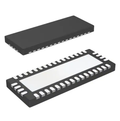
3.5 mm x 9 mm 42 Pin 0.5 mm pitch WQFN
package
•
•
•
•
•
•
•
•
•
•
•
•
•
2 Applications
•
•
•
•
•
•
•
Desktop PC/motherboard
Rack server
Microserver & tower server
High performance computing
Hardware accelerator
Network attached storage
Storage area network (SAN) & host bus adapter
(HBA) card
Network interface card (NIC)
•
The DS160PR412 receivers deploy continuous time
linear equalizers (CTLE) to provide a high-frequency
boost. The equalizer can open an input eye that is
completely closed due to inter-symbol interference
(ISI) induced by an interconnect medium, such as
PCB traces and cables. The linear redriver along with
the passive channel as a whole get link trained for
best transmit and receive equalization settings
resulting in best electrical link and lowest possible
latency. Low channel-channel cross-talk, low additive
jitter and excellent return loss allows the device to
become almost a passive element in the link. The
devices has internal linear voltage regulator to provide
clean power supply for high speed data paths that
provides high immunity to any supply noise on the
board.
The DS160PR412 implements high speed testing
during production for reliable high volume
manufacturing. The device also has low AC and DC
gain variation providing consistent equalization in high
volume platform deployment.
Device Information (1)
PART NUMBER
PACKAGE
DS160PR412
(1)
BODY SIZE (NOM)
WQFN (42)
3.5 mm x 9 mm
For all available packages, see the orderable addendum at
the end of the data sheet.
RX 8-ch
RX
4 Ch 2:1 Mux
TXB 8-ch
DS160PR412
TX 8-ch
CPU
Connector-A
Multiplexer
A
RX
A
8ch
PCIe Card
8ch
4 Ch 1:2 De-mux
x8
Slot
De-multiplexer
DS160PR421
RXB 8-ch
4-Ch
TX
4-Ch
x8
Connector-B
x8
Redriver Mux
4-Ch
DS160PR421
TX 1
TX 2
4-Ch
RX 1
4-Ch
RX 2
DS160PR412
4-Ch
Redriver Demux
TX
PCIe Card
x16
Slot
x8
PCIe Lane Muxing
Application Use Case
An©IMPORTANT
NOTICEIncorporated
at the end of this data sheet addresses availability, warranty, changes, use in
safety-critical
applications,
Copyright
2020 Texas Instruments
Submit
Document
Feedback
intellectual property matters and other important disclaimers. PRODUCTION DATA.
Product Folder Links: DS160PR412
1
�DS160PR412
www.ti.com
SNLS685 – DECEMBER 2020
Table of Contents
1 Features............................................................................1
2 Applications..................................................................... 1
3 Description.......................................................................1
4 Revision History.............................................................. 2
5 Pin Configuration and Functions...................................3
6 Specifications.................................................................. 6
6.1 Absolute Maximum Ratings ....................................... 6
6.2 ESD Ratings .............................................................. 6
6.3 Recommended Operating Conditions ........................6
6.4 Thermal Information ...................................................7
6.5 DC Electrical Characteristics ..................................... 7
6.6 High Speed Electrical Characteristics ........................8
6.7 SMBUS/I2C Timing Charateristics ............................. 9
6.8 Typical Characteristics.............................................. 11
7 Detailed Description......................................................14
7.1 Overview................................................................... 14
7.2 Functional Block Diagram......................................... 14
7.3 Feature Description...................................................14
7.4 Device Functional Modes..........................................16
7.5 Programming............................................................ 16
8 Application and Implementation.................................. 18
8.1 Application Information............................................. 18
8.2 Typical Applications.................................................. 18
9 Power Supply Recommendations................................23
10 Layout...........................................................................24
10.1 Layout Guidelines................................................... 24
11 Layout Example........................................................... 25
12 Device and Documentation Support..........................27
12.1 Receiving Notification of Documentation Updates..27
12.2 Support Resources................................................. 27
12.3 Trademarks............................................................. 27
12.4 Electrostatic Discharge Caution..............................27
12.5 Glossary..................................................................27
13 Mechanical, Packaging, and Orderable
Information.................................................................... 28
4 Revision History
NOTE: Page numbers for previous revisions may differ from page numbers in the current version.
2
DATE
REVISION
NOTES
December 2020
*
Advance Info.
Submit Document Feedback
Copyright © 2020 Texas Instruments Incorporated
Product Folder Links: DS160PR412
�DS160PR412
www.ti.com
SNLS685 – DECEMBER 2020
39 GND
39
40 EQ0/ADDR
40
41 MODE
41
42 RX_DET/SCL
42
5 Pin Configuration and Functions
GAIN/SDA
11
38
38 TXA0P
VREG1
22
37
37 TXA0N
RX0P
33
36
36 TXB0P
RX0N
44
35
35 TXB0N
VCC
55
34
34 TXA1P
GND
66
33
33 TXA1N
RX1P
77
32
32 TXB1P
RX1N
88
31
31 TXB1N
GND
99
EP=GND
30
30 GND
VREG2 12
12
27
27 TXB2P
VCC 13
13
26
26 TXB2N
RX3P 14
14
25
25 TXA3P
RX3N 15
15
24
24 TXA3N
GND 16
16
23
23 TXB3P
SEL 17
17
22
22 TXB3N
GND 21
21
28
28 TXA2N
EQ1 20
20
RX2N 11
11
19
RSVD 19
29
29 TXA2P
18
PD 18
RX2P 10
10
Figure 5-1. RUA Package 42-Pin WQFN Top View
Table 5-1. Pin Functions
PIN
NAME
MODE
I/O
NO.
41
I, 4-level
DESCRIPTION
Sets device control configuration modes. 4-level IO pin as defined in Table 7-3.
The pin can be exercised at device power up or in normal operation mode.
L0: Pin Mode – device control configuration is done solely by strap pins.
L1 or L2: SMBus/I2C Slave Mode – device control configuration is done by an
external controller with SMBus/I2C master. This pin along with ADDR pin sets
devices slave address.
L3 (Float): RESERVED – TI internal test mode.
Submit Document Feedback
Copyright © 2020 Texas Instruments Incorporated
Product Folder Links: DS160PR412
3
�DS160PR412
www.ti.com
SNLS685 – DECEMBER 2020
Table 5-1. Pin Functions (continued)
PIN
NAME
I/O
DESCRIPTION
In Pin Mode:
The EQ0 and EQ1 pins sets receiver linear equalization CTLE (AC gain) for all
channels according to Table 7-1. These pins are sampled at device power-up only.
In SMBus/I2C Mode:
The ADDR pin in conjunction with MODE pin sets SMBus / I2C slave address
according to Table 7-4. The pin is sampled at device power-up only.
EQ0 /ADDR
40
I, 4-level
EQ1
20
I, 4-level
GAIN /SDA
4
NO.
In Pin Mode:
DC gain (broadbad gain including high frequency) from the input to the output of
the device for all channels. Note the device also provides AC (high frequency)
gain in the form of equalization controlled by EQ pins or SMBus/I2C registers.
In SMBus/I2C Mode:
3.3 V SMBus/I2C data. External pullup resistor such as 4.7 kΩ required for
operation.
1
I, 4-level / IO
GND
EP, 6, 9, 16,
21, 30, 39
P
Ground reference for the device.
EP: the Exposed Pad at the bottom of the QFN package. It is used as the GND
return for the device. The EP should be connected to ground plane(s) through low
resistance path. A via array provides a low impedance path to GND. The EP also
improves thermal dissipation.
RSVD
19
O
TI internal test pin. Keep no connect.
PD
18
I, 3.3-V LVCMOS
RX_DET /SCL
42
I, 4-level / IO
RX0N
4
I
Inverting differential RX inputs. Channel 0.
RX0P
3
I
Noninverting differential RX inputs. Channel 0.
RX1N
8
I
Inverting differential RX inputs. Channel 1.
RX1P
7
I
Noninverting differential RX inputs. Channel 0.
RX2N
11
I
Inverting differential RX inputs. Channel 2.
RX2P
10
I
Noninverting differential RX inputs. Channel 2.
RX3N
15
I
Inverting differential RX inputs. Channel 3.
RX3P
14
I
Noninverting differential RX inputs. Channel 3.
SEL
17
I, 3.3 V LVCMOS
TXA0N
37
O
Inverting differential TX output – Port A, Channel 0.
TXA0P
38
O
Non-inverting differential TX output – Port A, Channel 0.
TXA1N
33
O
Inverting differential TX output – Port A, Channel 1.
TXA1P
34
O
Non-inverting differential TX output – Port A, Channel 1.
TXA2N
28
O
Inverting differential TX output – Port A, Channel 2.
TXA2P
29
O
Non-inverting differential TX output – Port A, Channel 2.
TXA3N
24
O
Inverting differential TX output – Port A, Channel 3.
TXA3P
25
O
Non-inverting differential TX output – Port A, Channel 3.
TXB0N
35
O
Inverting differential TX output – Port B, Channel 0.
2-level logic controlling the operating state of the redriver. Active in both Pin Mode
and SMBus/I2C Mode. The pin is used part of PCIe RX_DET state machine as
outlined in Table 7-2.
High: Power down for all channels
Low: Power up, normal operation for all channels
In Pin Mode:
Sets receiver detect state machine options according to Table 7-2. The pin is
sampled at device power-up only.
In SMBus/I2C Mode:
3.3 V SMBus/I2C clock. External pullup resistor such as 4.7 kΩ required for
operation.
Selects the mux path. Active in both Pin Mode and SMBus/I2C Mode. Note the
SEL pin must be exercised in system implementations for mux selection between
Port A vs Port B. The pin is used part of PCIe RX_DET state machine as outlined
in Table 7-2.
L: Port A selected.
H: Port B selected.
Submit Document Feedback
Copyright © 2020 Texas Instruments Incorporated
Product Folder Links: DS160PR412
�DS160PR412
www.ti.com
SNLS685 – DECEMBER 2020
Table 5-1. Pin Functions (continued)
PIN
NAME
NO.
I/O
DESCRIPTION
TXB0P
36
O
Non-inverting differential TX output – Port B, Channel 0.
TXB1N
31
O
Inverting differential TX output – Port B, Channel 1.
TXB1P
32
O
Non-inverting differential TX output – Port B, Channel 1.
TXB2N
26
O
Inverting differential TX output – Port B, Channel 2.
TXB2P
27
O
Non-inverting differential TX output – Port B, Channel 2.
TXB3N
22
O
Inverting differential TX output – Port B, Channel 3.
TXB3P
23
O
Non-inverting differential TX output – Port B, Channel 3.
5, 13
P
Power supply, VCC = 3.3 V ± 10%. The VCC pins on this device should be
connected through a low-resistance path to the board VCC plane.
VREG1
2
P
Internal regulator output. Must add decoupling capacitor of 0.22 µF near the pin.
Do not route the pin beyond the decoupling capacitor. Do not connect to VREG2.
Do not use as a power supply for any other component on the board.
VREG2
12
P
Internal regulator output. Must add decoupling caps of 0.22 µF near the pin. Do
not route the pin beyond the decoupling capacitor. Do not connect to VREG1. Do
not use as a power supply for any other component on the board.
VCC
Submit Document Feedback
Copyright © 2020 Texas Instruments Incorporated
Product Folder Links: DS160PR412
5
�DS160PR412
www.ti.com
SNLS685 – DECEMBER 2020
6 Specifications
6.1 Absolute Maximum Ratings
over operating free-air temperature range (unless otherwise noted)(1)
MIN
MAX
UNIT
VCCABSMAX
Supply Voltage (VCC)
–0.5
4.0
V
VIOCMOS,ABSMAX
3.3 V LVCMOS and Open Drain I/O voltage
–0.5
4.0
V
VIO4LVL,ABSMAX
4-level Input I/O voltage
–0.5
2.75
V
VIOHS-RX,ABSMAX
High-speed I/O voltage (RXnP, RXnN)
–0.5
3.2
V
VIOHS-TX,ABSMAX
High-speed I/O voltage (TXnP, TXnN)
–0.5
2.75
V
TJ,ABSMAX
Junction temperature
150
°C
Tstg
Storage temperature range
150
°C
(1)
–65
Stresses beyond those listed under Absolute Maximum Ratings may cause permanent damage to the device. These are stress ratings
only, which do not imply functional operation of the device at these or any other conditions beyond those indicated under
Recommended Operating Conditions. Exposure to absolute-maximum-rated conditions for extended periods may affect device
reliability.
6.2 ESD Ratings
VALUE
V(ESD)
(1)
(2)
Electrostatic discharge
Human body model (HBM), per ANSI/ESDA/JEDEC JS-001(1)
±2000
Charged device model (CDM), per JEDEC specification JESD22C101(2)
±500
UNIT
V
JEDEC document JEP155 states that 500-V HBM allows safe manufacturing with a standard ESD control process. Pins listed as ±2 kV
may actually have higher performance.
JEDEC document JEP157 states that 250-V CDM allows safe manufacturing with a standard ESD control process.
6.3 Recommended Operating Conditions
over operating free-air temperature range (unless otherwise noted)
VCC
Supply voltage, VCC to GND
NVCC
Supply noise tolerance1
TRampVCC
VCC supply ramp time
MIN
NOM
MAX
3.0
3.3
3.6
V
DC to 2.5 MHz, sinusoidal
6
From 0 V to 3.0 V
UNIT
10
mVpp
0.150
100
ms
TJ
Operating junction temperature
–40
125
°C
TA
Operating ambient temperature
–40
85
°C
PWLVCMOS
Minimum pulse width required for
the device to detect a valid signal PD, SEL
on LVCMOS inputs
200
VCCSMBUS
SMBus/I2C SDA and SCL Open
Drain Termination Voltage
FSMBus
SMBus/I2C clock (SCL) frequency
in SMBus slave mode
VIDLAUNCH
Source differential launch
amplitude
Supply voltage for open drain
pull-up resistor
Submit Document Feedback
uS
3.6
V
10
400
kHz
800
1200
mVpp
Copyright © 2020 Texas Instruments Incorporated
Product Folder Links: DS160PR412
�DS160PR412
www.ti.com
SNLS685 – DECEMBER 2020
6.4 Thermal Information
DS160PR41
2,
DS160PR42
1
THERMAL METRIC(1)
UNIT
RUA, 42
Pins
RθJA-High
26.1
℃/W
RθJC(top) Junction-to-case (top) thermal resistance
14.1
℃/W
RθJB
Junction-to-board thermal resistance
8.7
℃/W
ψJT
Junction-to-top characterization parameter
1.6
℃/W
ψJB
Junction-to-board characterization parameter
8.6
℃/W
RθJC(bot) Junction-to-case (bottom) thermal resistance
2.6
℃/W
K
(1)
Junction-to-ambient thermal resistance
For more information about traditional and new thermal metrics, see the IC Package Thermal Metrics application report.
6.5 DC Electrical Characteristics
over operating free-air temperature and voltage range (unless otherwise noted)
PARAMETER
TEST CONDITIONS
MIN
TYP
MAX
UNIT
Power
GAIN1/0 = L3
120
mW
GAIN1/0 = L0
110
mW
POWERCH
Active power per channel
IACTIVE
Device current consumption when four
GAIN1/0 = L3, PD = L
channels are active
ISTBY
VREG
145
190
mA
Device current consumption in standby
All channels disabled (PD = H)
power mode
30
45
mA
Internal regulator output
2.5
V
Control IO
VIH
High level input voltage
SDA, SCL, PD, SEL pins
VIL
Low level input voltage
SDA, SCL, PD, SEL pins
2.1
V
VOH
High level output voltage
Rpull-up = 4.7 kΩ (SDA, SCL pins)
VOL
Low level output voltage
IOL = –4 mA (SDA, SCL pins)
IIH,SEL
Input high leakage current for SEL pin
VInput = VCC
80
µA
IIH
Input high leakage current
VInput = VCC, (SCL, SDA, PD pins)
10
µA
IIL
Input low leakage current
VInput = 0 V, (SCL, SDA, PD, SEL pins)
IIH,FS
Input high leakage current for fail safe
input pins
VInput = 3.6 V, VCC = 0 V, (SCL, SDA,
PD, SEL pins)
CIN-CTRL
Input capacitance
SDA, SCL, PD, SEL pins
1.08
2.1
V
V
0.4
-10
V
µA
150
1.5
µA
pF
4 Level IOs (MODE, GAIN, EQ0, EQ1, RX_DET pins)
IIH_4L
Input high leakage current, 4 level IOs VIN = 2.5 V
IIL_4L
Input low leakage current for all 4 level
VIN = GND
IOs except MODE.
IIL_4L,MODE
Input low leakage current for MODE
pin
VIN = GND
VRX-DC-CM
RX DC Common Mode (CM) Voltage
Device is in active or standby state
ZRX-DC
Rx DC Single-Ended Impedance
ZRX-HIGH-IMP-
DC input CM input impedance during
Inputs are at CM voltage
Reset or power-down
10
µA
-10
µA
-200
µA
Receiver
DC-POS
20
2.5
V
50
Ω
kΩ
Transmitter
Submit Document Feedback
Copyright © 2020 Texas Instruments Incorporated
Product Folder Links: DS160PR412
7
�DS160PR412
www.ti.com
SNLS685 – DECEMBER 2020
over operating free-air temperature and voltage range (unless otherwise noted)
PARAMETER
ZTX-DIFF-DC
DC Differential Tx Impedance
VTX-DC-CM
Tx DC common mode Voltage
ITX-SHORT
TEST CONDITIONS
MIN
Impedance of Tx during active
signaling, VID,diff = 1Vpp
TYP
UNIT
100
Ω
0.75
V
Total current the Tx can supply when
shorted to GND
Tx Short Circuit Current
MAX
90
mA
6.6 High Speed Electrical Characteristics
over operating free-air temperature and voltage range (unless otherwise noted)
PARAMETER
TEST CONDITIONS
MIN
TYP
MAX
UNIT
Receiver
RLRX-DIFF
XTRX
50 MHz to 1.25 GHz
-25
dB
1.25 GHz to 2.5 GHz
-22
dB
2.5 GHz to 4.0 GHz
-21
dB
4.0 GHz to 8.0 GHz
-14
dB
Receive-side pair-to-pair isolation
Pair-to-pair isolation (SDD21) between
two adjacent active receiver pairs from
10 MHz to 8 GHz.
-47
dB
Tx AC Peak-to-Peak Common Mode
Voltage
Measured with lowest EQ, GAIN = L3;
PRBS-7, 16 Gbps, over at least
106 bits using a bandpass-Pass Filter
from 30 Khz - 500 Mhz
Absolute Delta of DC Common Mode
Voltage during L0 and Electrical Idle
VTX-CM-DC = |VOUTn+ + VOUTn–|/2,
Measured by taking the absolute
difference of VTX-CM-DC during PCIe
state L0 and Electrical Idle
Absolute Delta of DC Common Mode
Voltage between VOUTn+ and VOUTn–
during L0
Measured by taking the absolute
difference of VOUTn+ and VOUTn– during
PCIe state L0
Input differential return loss
Transmitter
VTX-AC-CM-PP
VTX-CM-DCACTIVE-IDLEDELTA
VTX-CM-DCLINE-DELTA
0
50
mVpp
100
mV
10
mV
VTX-IDLE-DIFF- AC Electrical Idle Differential Output
Voltage
Measured by taking the absolute
difference of VOUTn+ and VOUTn– during
Electrical Idle, Measured with a bandpass filter consisting of two first-order
filters. The High-Pass and Low-Pass
-3-dB bandwidths are 10 kHz and 1.25
GHz, respectively - zero at input
0
10
mV
VTX-IDLE-DIFF- DC Electrical Idle Differential Output
Voltage
Measured by taking the absolute
difference of VOUTn+ and VOUTn– during
Electrical Idle, Measured with a firstorder Low-Pass Filter with –3-dB
bandwidth of 10 kHz
0
5
mV
Measured while Tx is sensing whether
a low-impedance Receiver is present.
No load is connected to the driver
output
0
600
mV
AC-p
DC
VTX-RCVDETECT
RLTX-DIFF
XTTX
Amount of Voltage change allowed
during Receiver Detection
Output differential return loss
Transmit-side pair-to-pair isolation
50 MHz to 1.25 GHz
-20
dB
1.25 GHz to 2.5 GHz
-18
dB
2.5 GHz to 4.0 GHz
-18
dB
4.0 GHz to 8.0 GHz
-16
dB
Minimum pair-to-pair isolation
(SDD21) between two adjacent active
transmitter pairs from 10 MHz to 8
GHz.
-48
dB
Device Datapath
8
Submit Document Feedback
Copyright © 2020 Texas Instruments Incorporated
Product Folder Links: DS160PR412
�DS160PR412
www.ti.com
SNLS685 – DECEMBER 2020
over operating free-air temperature and voltage range (unless otherwise noted)
PARAMETER
TEST CONDITIONS
MIN
TYP
MAX
UNIT
80
110
ps
20
ps
TPLHD/PHLD
Input-to-output latency (propagation
delay) through a data channel
For either Low-to-High or High-to-Low
transition
LTX-SKEW
Lane-to-Lane Output Skew
Between any two lanes within a single
transmitter.
Additive Random Jitter with data
Difference between through redriver
and baseline setup. 16Gbps PRBS15.
Minimal input/output
channels. Minimum EQ. 800 mVpp-diff
input swing.
70
fs
Intrinsic additive Random Jitter with
clock
Difference between through redriver
and baseline setup. 8 Ghz CK.
Minimal input/output
channels. Minimum EQ. 400 mVpp-diff
input swing.
90
fs
Additive Total Jitter with data
Difference between through redriver
and baseline setup. 16 Gbps PRBS15.
Minimal input/output
channels. Minimum EQ. 800 mVpp-diff
input swing.
4
ps
Intrinsic additive Total Jitter with clock
Difference between through redriver
and baseline setup. 8 Ghz CK.
Minimal input/output
channels. Minimum EQ. 800 mVpp-diff
input swing.
1
ps
-4.2
dB
Minimum EQ, GAIN = L1
-1.8
dB
Minimum EQ, GAIN = L2
0.25
dB
2.0
dB
17
dB
TRJ-DATA
TRJ-INTRINSIC
JITTERTOTALDATA
JITTERTOTALINTRINSIC
-20
Minimum EQ, GAIN = L0
DCGAIN
DC flat gain input to output
EQ-MAX8G
EQ boost at max setting (EQ INDEX = AC gain at 8 GHz relative to gain at
15)
100 MHz.
DCGAINVAR
DC gain variation
GAIN = L2, minimum EQ setting. MaxMin.
-2.3
1.7
dB
EQGAINVAR
EQ boost variation
At 8 Ghz. GAIN1/0 = L2, maximum EQ
setting. Max-Min.
-3.3
3.7
dB
LINDC
Output DC Linearity
GAIN = L3 (defauult). 128T pattern at
2.5 Gbps.
1000
mVpp
LINAC
Output AC Linearity
GAIN = L3 (default). 1T pattern at 16
Gbps.
750
mVpp
Minimum EQ, GAIN = L3 (Float)
6.7 SMBUS/I2C Timing Charateristics
over operating free-air temperature range (unless otherwise noted)
PARAMETER
TEST CONDITIONS
MIN
TYP
MAX
UNIT
Slave Mode
tSP
Pulse width of spikes which must be
suppressed by the input filter
tHD-STA
Hold time (repeated) START condition.
After this period, the first clock pulse is
generated
0.6
µs
tLOW
LOW period of the SCL clock
1.3
µs
THIGH
HIGH period of the SCL clock
0.6
µs
tSU-STA
Set-up time for a repeated START
condition
0.6
µs
tHD-DAT
Data hold time
0
µs
TSU-DAT
Data setup time
0.1
µs
50
ns
Submit Document Feedback
Copyright © 2020 Texas Instruments Incorporated
Product Folder Links: DS160PR412
9
�DS160PR412
www.ti.com
SNLS685 – DECEMBER 2020
over operating free-air temperature range (unless otherwise noted)
PARAMETER
TEST CONDITIONS
MIN
TYP
MAX
UNIT
tr
Rise time of both SDA and SCL
signals
tf
Fall time of both SDA and SCL signals Pull-up resistor = 4.7 kΩ, Cb = 10pF
tSU-STO
Set-up time for STOP condition
0.6
µs
tBUF
Bus free time between a STOP and
START condition
1.3
µs
tVD-DAT
Data valid time
0.9
µs
tVD-ACK
Data valid acknowledge time
0.9
µs
Cb
capacitive load for each bus line
400
pF
10
Pull-up resistor = 4.7 kΩ, Cb = 10pF
Submit Document Feedback
120
ns
2
ns
Copyright © 2020 Texas Instruments Incorporated
Product Folder Links: DS160PR412
�DS160PR412
www.ti.com
SNLS685 – DECEMBER 2020
6.8 Typical Characteristics
Equalization Boost vs Frequency
20
18
16
EQ=0
EQ=1
EQ=2
EQ=3
EQ=4
EQ=5
EQ=6
EQ=7
EQ=8
EQ=9
EQ=10
EQ=11
EQ=12
EQ=13
EQ=14
EQ=15
14
EQ Boost (dB)
12
10
8
6
4
2
0
-2
-4
0.1
1
10
Frequency (GHz)
Figure 6-1. Typical EQ Boost vs Frequency
Equalization over Voltage and Temperature (EQ=15)
22
VCC=3.3V, Temp=25C
VCC=3.3V, Temp=-40C
VCC=3.3V, Temp=85C
20
VCC=3.0V, Temp=25C
VCC=3.0V, Temp=-40C
VCC=3.0V, Temp=85C
VCC=3.6V, Temp=25C
VCC=3.6V, Temp=-40C
VCC=3.6V, Temp=85C
18
16
EQ Boost (dB)
14
12
10
8
6
4
2
0
0.1
1
10
Frequency (GHz)
Figure 6-2. Typical EQ Boost over Voltage and Temperature with EQ=15
Submit Document Feedback
Copyright © 2020 Texas Instruments Incorporated
Product Folder Links: DS160PR412
11
�DS160PR412
www.ti.com
SNLS685 – DECEMBER 2020
Input (RX) Differential Return Loss
0
-4
SDD11 Magnitude (dB)
-8
-12
-16
-20
-24
-28
SDD11
-32
PCIe 4.0 Mask
-36
0
2
4
6
8
10
12
Frequency (GHz)
14
16
18
20
Figure 6-3. Typical RX Differential Return Loss
Output (TX) Differential Return Loss
0
-4
SDD22 Magnitude (dB)
-8
-12
-16
-20
-24
-28
SDD22
-32
PCIe 4.0 Mask
-36
0
2
4
6
8
10
12
Frequency (GHz)
14
16
18
20
Figure 6-4. Typical TX Differential Return Loss
12
Submit Document Feedback
Copyright © 2020 Texas Instruments Incorporated
Product Folder Links: DS160PR412
�DS160PR412
www.ti.com
SNLS685 – DECEMBER 2020
Figure 6-5. Typical Jitter Characteristics - Top: 16Gbps PRBS15 Input to the Device, Bottom: Output of
the Device.
Submit Document Feedback
Copyright © 2020 Texas Instruments Incorporated
Product Folder Links: DS160PR412
13
�DS160PR412
www.ti.com
SNLS685 – DECEMBER 2020
7 Detailed Description
7.1 Overview
The DS160PR412 is a four channel linear redriver with ingrated demultiplexer (demux). The low-power highperformance linear repeater or redriver is designed to support PCIe 1.0/2.0/3.0/4.0. The device is a protocol
agnostic linear redriver that can operate for interfaces up to 16 Gbps.
The DS160PR412 can be configured two different ways:
Pin Mode – device control configuration is done solely by strap pins. Pin mode is expected to be good enough
for many system implementation needs.
SMBus/I2C Slave Mode - provides most flexibility. Requires a SMBus/I2C master device to configure
DS160PR412 though writing to its slave address.
7.2 Functional Block Diagram
One of Four 1:2 Demultiplexer Modules
Term
Term
RXnP
CTLE
RXnN
DS160PR412
Redriver Demux 1:2
Linear
Driver
TXAnP
Linear
Driver
TXBnP
TXAnN
TXBnN
RX Detect
Select
mux
control
CTLE
Control
VCC
Driver
Control
RX Detect
Term
RX
Detect
Control
Voltage Regulator
VREG1,2
Shared Digital Core
PowerOn Reset
Always-On
10MHz
GAIN/SDA
RX_DET/SCL
SEL
EQ1
PD
MODE
EQ0/ADDR
Shared Digital
GND
7.3 Feature Description
7.3.1 Linear Equalization
The DS160PR412 receivers feature a continuous-time linear equalizer (CTLE) that applies high-frequency boost
to help equalize the frequency-dependent insertion loss effects of the passive channel. Table 7-1 shows
available equalization boost through EQ control pins (EQ1 and EQ0), when in Pin Control mode (MODE = L0).
14
Submit Document Feedback
Copyright © 2020 Texas Instruments Incorporated
Product Folder Links: DS160PR412
�DS160PR412
www.ti.com
SNLS685 – DECEMBER 2020
Table 7-1. Equalization Control Settings
EQUALIZATION SETTING
EQ INDEX
TYPICAL EQ BOOST (dB)
EQ1_0 (Ch 0-3) / EQ1_1 (Ch EQ0_0 (Ch0-3) / EQ0_1 (Ch
4-7)
4-7)
0
L0
L0
@ 4 GHz
@ 8 GHz
0.0
-0.1
1
L0
L1
1.5
4.5
2
L0
L2
2.0
5.5
3
L0
L3
2.5
6.5
4
L1
L0
2.7
7.0
5
L1
L1
3.0
8.0
6
L1
L2
4.0
9.0
7
L1
L3
5.0
10.0
8
L2
L0
6.0
11.0
9
L2
L1
7.0
12.0
10
L2
L2
7.5
12.5
11
L2
L3
8.0
13.0
12
L3
L0
8.5
14.0
13
L3
L1
9.5
15.0
14
L3
L2
10.0
16.0
15
L3
L3
11.0
17.0
The equalization of the device can also be set by writing to SMBus/I2C registers in slave mode. Refer to the
DS160PR412/421 Programming Guide for details.
7.3.2 Flat Gain
The GAIN pin can be used to set the overall datapath flat gain (broadbabd gain including high frequency) of the
DS160PR412 when the device is in Pin Mode. The default recommendation for most systems will be GAIN = L3
(float).
The flat gain and equalization of the DS160PR412 must be set such that the output signal swing at DC and high
frequency does not exceed the DC and AC linearity ranges of the devices, respectively.
Note the device also provides AC (high frequency) gain in the form of equalization controlled by EQ pins or
SMBus/I2C registers.
7.3.3 Receiver Detect State Machine
The DS160PR412 deploys an RX detect state machine that governs the RX detection cycle as defined in the
PCI express specifications. At device power up or through manually triggered event using PD or SEL pin or
writing to the relevant I2C/SMBus register, the redriver determines whether or not a valid PCI express
termination is present at the far end of the link. The RX_DET pin of DS160PR412 provides additional flexibility
for system designers to appropriately set the device in desired mode according to Table 7-2. For the PCIe
application the RX_DET pin can be left floating for default settings.
Note power up ramp or PD/SEL event triggers RX detect for all four channels. In applications where
DS160PR412 channels are used for multiple PCIe links, the RX detect function can be performed for individual
channels through writing in appropriate I2C/SMBus registers.
Table 7-2. Receiver Detect State Machine Settings
PD
L
RX_DET
RX Common-mode Impedance
L0
Always 50 Ω
COMMENTS
PCI Express RX detection state machine is disabled.
Recommended for non PCIe interface use case where the
DS160PR412 is used as buffer with equalization.
Submit Document Feedback
Copyright © 2020 Texas Instruments Incorporated
Product Folder Links: DS160PR412
15
�DS160PR412
www.ti.com
SNLS685 – DECEMBER 2020
Table 7-2. Receiver Detect State Machine Settings (continued)
PD
RX_DET
RX Common-mode Impedance
COMMENTS
L
L3 (Float)
Pre Detect: Hi-Z
Post Detect: 50 Ω.
TX polls every ≈150 µs until valid termination is detected. RX CM
impedance held at Hi-Z until detection Reset by asserting PD high
for 200 µs then low.
H
X
Hi-Z
Reset Channels 0-3 signal path and set their RX impedance to HiZ
L
X
Pre Detect: Hi-Z
Post Detect: 50 Ω.
Reset Channels 4-7 signal path and set their RX impedance to HiZ.
H
X
Hi-Z
7.4 Device Functional Modes
7.4.1 Active PCIe Mode
The device is in normal operation with PCIe state machine enabled by RX_DET = L3 (float). This mode is
recommended for PCIe use cases. In this mode PD pin is driven low in a system (for example by PCIe connector
"PRSNT" signal). In this mode, the device redrives and equalizes PCIe RX or TX signals to provide better signal
integrity.
7.4.2 Active Buffer Mode
The device is in normal operation with PCIe state machine disabled by RX_DET = L0. This mode is
recommended for non-PCIe use cases. In this mode the device is working as a buffer to provide linear
equalization to improve signal integrity.
7.4.3 Standby Mode
The device is in standby mode invoked by PD = H. In this mode, the device is in standby mode conserving
power.
7.5 Programming
7.5.1 Control and Configuration Interface
7.5.1.1 Pin Mode
The DS160PR412 can be fully configured through pin-strap pins. In this mode the device uses 2-level and 4level pins for device control and signal integrity optimum settings.
7.5.1.1.1 Four-Level Control Inputs
The DS160PR412 has five (EQ0, EQ1, GAIN, MODE, and RX_DET) 4-level inputs pins that are used to control
the configuration of the device. These 4-level inputs use a resistor divider to help set the 4 valid levels and
provide a wider range of control settings. External resistors must be of 10% tolerance or better. The EQ0, EQ1,
GAIN, and RX_DET pins are sampled at power-up only. The MODE pin can be exercised at device power up or
in normal operation mode.
Table 7-3. 4-Level Control Pin Settings
LEVEL
SETTING
L0
1 kΩ to GND
L1
13 kΩ to GND
L2
59 kΩ to GND
L3
F (Float)
7.5.1.2 SMBUS/I2C Register Control Interface
If MODE = L2 (SMBus / I2C slave control mode), the DS160PR412 is configured for best signal integrity through
a standard I2C or SMBus interface that may operate up to 400 kHz. The slave address of the DS160PR412 is
determined by the pin strap settings on the ADDR and MODE pins. The eight possible slave addresses (7-bit) for
each channel banks of the device are shown in Table 7-4. In SMBus/I2C modes the SCL, SDA pins must be
16
Submit Document Feedback
Copyright © 2020 Texas Instruments Incorporated
Product Folder Links: DS160PR412
�DS160PR412
www.ti.com
SNLS685 – DECEMBER 2020
pulled up to a 3.3 V supply with a pull-up resistor. The value of the resistor depends on total bus capacitance.
4.7 kΩ is a good first approximation for a bus capacitance of 10 pF.
Refer to the DS160PR412/421 Programming Guide for details.
Table 7-4. SMBUS/I2C Slave Address Settings
MODE
ADDR
7-bit Slave Address Channels 0-1
7-bit Slave Address Channels 2-3
L1
L0
0x18
0x19
L1
L1
0x1A
0x1B
L1
L2
0x1C
0x1D
L1
L3
0x1E
0x1F
L2
L0
0x20
0x21
L2
L1
0x22
0x23
L2
L2
0x24
0x25
L2
L3
0x26
0x27
Submit Document Feedback
Copyright © 2020 Texas Instruments Incorporated
Product Folder Links: DS160PR412
17
�DS160PR412
www.ti.com
SNLS685 – DECEMBER 2020
8 Application and Implementation
Note
Information in the following applications sections is not part of the TI component specification, and TI
does not warrant its accuracy or completeness. TI’s customers are responsible for determining
suitability of components for their purposes. Customers should validate and test their design
implementation to confirm system functionality.
8.1 Application Information
The DS160PR412 is a high-speed linear repeater with integrated demux . The device extends the reach of a
differential channels impaired by loss from transmission media like PCBs and cables. It can be deployed in a
variety of different systems. The following sections outline typical applications and their associated design
considerations.
8.2 Typical Applications
The DS160PR412 is a PCI Express linear redriver that can also be configured as interface agnostic redriver by
disabling its RX detect feature. The device can be used in wide range of interfaces including:
• PCI Express
• Ultra Path Interconnect (UPI)
• SATA
• SAS
• Display Port
18
Submit Document Feedback
Copyright © 2020 Texas Instruments Incorporated
Product Folder Links: DS160PR412
�DS160PR412
www.ti.com
SNLS685 – DECEMBER 2020
8.2.1 PCIe x8 Lane Switching
The DS160PR412 and DS160PR421 and can be used in desktop motherboard applications to switch PCIe lanes
from a CPU in to one of the two PCIe CEM connectors. Figure 8-1 shows a simplified schematic for the
configuration. Two DS160PR412 demultiplex eight TX channels from CPU into one of the two PCIe slots. On the
other hand two DS160PR421 multiplex eight RX channels from one of the two PCIe slots to CPU.
Two PR412
Mux selection
Float
SEL
RX_DET
RXnP
8 TX Chan
X8 Slot
Linear
Driver
CTLE
TXAnP
RXnN
TXAnN
8 Lanes
System Level
Power Control
1 of 4
channels
PD
Linear
Driver
TXBnP
TXBnN
GPIO mode
GND
MODE
1 NŸ
GAIN
DS160PR412
Pin strap to
fine tune
EQ gain
settings
EQ0
PCIe Redriver Demux
EQ1
VCC
VREG2
VREG1
PCIe
Slot
A
pin strap control
for DC gain
VCC
1 F
0.1 F
(2x)
Minimum
recommended
decoupling
0.1 F
0.1 F
Two PR421
Mux selection
CPU
(root
complex)
SEL
Float
RX_DET
8 RX Chan
Linear
Driver
TXnP
CTLE
TXnN
RXAnP
RXAnN
System Level
Power Control
CTLE
PD
RXBnP
RXBnN
Optional pin strap
control for DC gain
GAIN
Pin strap to
fine tune
EQ gain
settings
8 Lanes
1 of 4
channels
MODE
DS160PR421
PCIe Redriver Mux
EQ0
1 NŸ
EQ1
VREG1
VREG2
0.1 F
0.1 F
VCC
0.1 F
(2x)
PCIe
Slot
B
GPIO mode
GND
VCC
Minimum
recommended
decoupling
1 F
8 Lanes
X16 Slot
Figure 8-1. Simplified Schematic for PCIe Lane Switching for PC Desktop Application
Submit Document Feedback
Copyright © 2020 Texas Instruments Incorporated
Product Folder Links: DS160PR412
19
�DS160PR412
www.ti.com
SNLS685 – DECEMBER 2020
8.2.1.1 Design Requirements
As with any high-speed design, there are many factors which influence the overall performance. The following
list indicates critical areas for consideration during design.
• Use 85 Ω impedance traces when interfacing with PCIe CEM connectors. Length matching on the P and N
traces should be done on the single-ended segments of the differential pair.
• Use a uniform trace width and trace spacing for differential pairs.
• Place AC-coupling capacitors near to the receiver end of each channel segment to minimize reflections.
• For Gen 3.0 and Gen 4.0, AC-coupling capacitors of 220 nF are recommended, set the maximum body size
to 0402, and add a cutout void on the GND plane below the landing pad of the capacitor to reduce parasitic
capacitance to GND.
• Back-drill connector vias and signal vias to minimize stub length.
• Use reference plane vias to ensure a low inductance path for the return current.
8.2.1.2 Detailed Design Procedure
In PCIe Gen 4.0 and Gen 3.0 applications, the specification requires Rx-Tx link training to establish and optimize
signal conditioning settings at 16 Gbps and 8 Gbps, respectively. In link training, the Rx partner requests a series
of FIR – pre-shoot and de-emphasis coefficients (10 Presets) from the Tx partner. The Rx partner includes 7levels (6 dB to 12 dB) of CTLE followed by a single tap DFE. The link training would pre-condition the signal,
with an equalized link between the root-complex and endpoint.
Note that there is no link training in PCIe Gen 1.0 (2.5 Gbps) or PCIe Gen 2.0 (5.0 Gbps) applications. The
DS160PR412 is placed in between the Tx and Rx. It helps extend the PCB trace reach distance by boosting the
attenuated signals with its equalization, which allows the user to recover the signal by the downstream Rx more
easily.
For operation in Gen 4.0 and Gen 3.0 links, the DS160PR412 transmit outputs are designed to pass the Tx
Preset signaling onto the Rx for the PCIe Gen 4.0 or Gen 3.0 link to train and optimize the equalization settings.
The suggested setting for the device is GAIN = L3 (default). Adjustments to the EQ setting should be performed
based on the channel loss to optimize the eye opening in the Rx partner. The Tx equalization presets or CTLE
and DFE coefficients in the Rx can also be adjusted to further improve the eye opening.
8.2.1.3 Pin-to-pin Passive versus Redriver Option
For eight lane PCIe lane muxing application a topology is illustrated where two DS160PR412 and two
DS160PR421 are used. There are system use cases where the PCIe link loss is low enough that a signal
conditioner such as linear redrivers may not be needed. In such use cases system engineers may consider
passive mux to achieve same lane muxing topology. The four channel passive mux/demux TMUXHS4412 is pinto-pin (p2p) compatible with the DS160PR412 and DS160PR421 . This p2p component availability provides
great flexibility for system implementation engineers where the need for redriver is not completely clear. Figure
8-2 illustrates p2p passive vs redriver option to implement PCIe lane switching.
PCIe Card
x16
Slot
PCIe Card
x16
Slot
x8
Connector-B
x8
Connector-B
x8
x8
TMUXHS4412
RXB 8-ch
RX 8-ch
DS160PR421
RXB 8-ch
4 Ch 2:1 Mux
Connector-A
x8
Passive option
CPU
TXB 8-ch
Pin-2-pin
DS160PR412
CPU
A
Connector-A
8ch
A
8ch
PCIe Card
x8
Slot
TX 8-ch
4 Ch 1:2 redriver demux
A
RX
TX
A
8ch
PCIe Card
x8
Slot
TX 8-ch
8ch
4 Ch 1:2 demux
RX
TMUXHS4412
TX
TXB 8-ch
RX 8-ch
4 Ch 2:1 redriver mux
x8
Redriver option
Figure 8-2. Pin-to-pin passive vs redriver option for PCIe lane switching
20
Submit Document Feedback
Copyright © 2020 Texas Instruments Incorporated
Product Folder Links: DS160PR412
�DS160PR412
www.ti.com
SNLS685 – DECEMBER 2020
8.2.1.4 Application Curves
The DS160PR412 is a linear redriver that can be used to extend channel reach of a PCIe link. Normally, PCIecompliant TX and RX are equipt with signal-conditioning functions and can handle channel losses of up to 28 dB
at 8 GHz. In real implementation the channel reach is often lower. With the DS160PR412 in the link, the total
channel loss between a PCIe root complex and an end-point can be extended up to 42 dB at 8 GHz.
Figure 8-3 shows an electric link that models a single channel of a PCIe link and eye diagrams measured at
different locations along the link. The source that models a PCIe Transmitter sends a 16 Gbps PRBS-15 signal
with P7 presets. After a transmission channel with –30 dB at 8 GHz insertion loss, the eye diagram is fully
closed. The DS160PR412 with its CTLE set to the maximum (17 dB boost) together with the source TX
equalization compensates for the losses of the pre-channel (TL1) and opens the eye at the output of the device.
The post-channel (TL2) losses mandate the use of PCIe RX equalization functions such as CTLE and DFE that
are normally available in a PCIe-compliant receiver.
CPU / PCIe RC
16 Gbps, PRBS15
800mV
Pre-Cursor: 3.5 dB
Post-Cursor: -6 dB
TL1
-30 dB @ 8 GHz
DUT
PCIe 4.0 Redriver
PCIe
End Point
TL2
-15 dB @ 8 GHz
RX CTLE:
12 dB
RX EQ = 15 (17 dB)
Figure 8-3. PCIe 4.0 Link Reach Extension Using the DS160PR412
Submit Document Feedback
Copyright © 2020 Texas Instruments Incorporated
Product Folder Links: DS160PR412
21
�DS160PR412
www.ti.com
SNLS685 – DECEMBER 2020
8.2.2 DisplayPort Application
The DS160PR412 can be used as a four channel DisplayPort (DP) redriver demux for data rates up to 20 Gbps.
To use the device in a non-PCIe application, the RX_DET pin must be pin-strapped to GND with 1 kΩ resistor
(L0).
The inverted DisplayPort HPD signal can be used to put the device into standby mode by using its PD pin. Note
in a DisplayPort link a sink can use HPD line to create an interrupt for its link partner source. If HPD signal is
used for power management an RC filter must be installed to filter out HPD interrupt signals.
The device is a linear redriver which is agnostic to DP link training. The DP link training negotiation between a
display source and sink stays effective through the device . The redriver becomes part of the electrical channel
along with passive traces, cables, and so forth, resulting into optimum source and sink parameters for best
electrical link.
Figure 8-4 shows a simplified schematic for DisplayPort demultiplexing application using DS160PR412. Auxiliary
and Hot plug detect (HPD) are demuxed outside of DS160PR412. If system use case requires implementing DP
power states, the device must be controlled by the I2C or the pin-strap pins.
AUXAp
For brevity AUX
biasing is not shown
AUXAn
AUXp
TS3A5223
HPDA
AUXn
HPD
2-Ch 2:1 mux
AUXBp
AUXBn
HPDB
AUXAp
Demux control
AUXAn
SEL
RX_DET
1k
GND
RXnP
Linear
Driver
CTLE
DisplayPort
Sink A
AUXBp
DisplayPort
Sink B
TXAnP
TXAnN
RXnN
DisplayPort
Source
HPDA
3.3V
59k
AUXp
PD
Linear
Driver
1 of 4
channels
TXBnP
TXBnN
AUXn
HPD
0.1 F
AUXBn
GPIO mode
100k
HPD
GND
HPDB
MODE
DS160PR412
DP Main Link Redriver
1:2 Demux
1 NŸ
GAIN
EQ0
VCC
VCC
1 F
Minimum
recommended
decoupling
0.1 F
(2x)
VREG1
0.1 F
EQ1
VREG2
Optional pin strap
control for DC gain
Pin strap to fine tune
EQ gain settings
0.1 F
Figure 8-4. Simplified Schematic for DisplayPort Demultiplexer Application
22
Submit Document Feedback
Copyright © 2020 Texas Instruments Incorporated
Product Folder Links: DS160PR412
�DS160PR412
www.ti.com
SNLS685 – DECEMBER 2020
9 Power Supply Recommendations
Follow these general guidelines when designing the power supply:
1. The power supply should be designed to provide the operating conditions outlined in the recommended
operating conditions section in terms of DC voltage, AC noise, and start-up ramp time.
2. The DS160PR412 does not require any special power supply filtering, such as ferrite beads, provided that the
recommended operating conditions are met. Only standard supply decoupling is required. Typical supply
decoupling consists of a 0.1 µF capacitor per VCC pin, one 1.0 µF bulk capacitor per device, and one 10 µF
bulk capacitor per power bus that delivers power to one or more devices. The local decoupling (0.1 µF)
capacitors must be connected as close to the VCC pins as possible and with minimal path to the device
ground pad.
3. The DS160PR412 voltage regulator output pins require decoupling caps of 0.1 µF near each pins. The
regulator is only for internal use. Do not use to provide power to any external component.
Submit Document Feedback
Copyright © 2020 Texas Instruments Incorporated
Product Folder Links: DS160PR412
23
�DS160PR412
www.ti.com
SNLS685 – DECEMBER 2020
10 Layout
10.1 Layout Guidelines
The following guidelines should be followed when designing the layout:
1. Decoupling capacitors should be placed as close to the VCC pins as possible. Placing the decoupling
capacitors directly underneath the device is recommended if the board design permits.
2. High-speed differential signals TXnP/TXnN and RXnP/RXnN should be tightly coupled, skew matched, and
impedance controlled.
3. Vias should be avoided when possible on the high-speed differential signals. When vias must be used, take
care to minimize the via stub, either by transitioning through most/all layers or by back drilling.
4. GND relief can be used (but is not required) beneath the high-speed differential signal pads to improve signal
integrity by counteracting the pad capacitance.
5. GND vias should be placed directly beneath the device connecting the GND plane attached to the device to
the GND planes on other layers. This has the added benefit of improving thermal conductivity from the device
to the board.
24
Submit Document Feedback
Copyright © 2020 Texas Instruments Incorporated
Product Folder Links: DS160PR412
�DS160PR412
www.ti.com
SNLS685 – DECEMBER 2020
11 Layout Example
Figure 11-1 shows DS160PR412 layout example.
Figure 11-1. DS160PR412 layout example
Figure 11-2 shows a layout illustration where two DS160PR412 and two DS160PR421 are used to switch 8
lanes between two PCIe slots.
Submit Document Feedback
Copyright © 2020 Texas Instruments Incorporated
Product Folder Links: DS160PR412
25
�DS160PR412
www.ti.com
SNLS685 – DECEMBER 2020
Figure 11-2. Layout example for PCIe lane muxing application
26
Submit Document Feedback
Copyright © 2020 Texas Instruments Incorporated
Product Folder Links: DS160PR412
�DS160PR412
www.ti.com
SNLS685 – DECEMBER 2020
12 Device and Documentation Support
12.1 Receiving Notification of Documentation Updates
To receive notification of documentation updates, navigate to the device product folder on ti.com. Click on
Subscribe to updates to register and receive a weekly digest of any product information that has changed. For
change details, review the revision history included in any revised document.
12.2 Support Resources
TI E2E™ support forums are an engineer's go-to source for fast, verified answers and design help — straight
from the experts. Search existing answers or ask your own question to get the quick design help you need.
Linked content is provided "AS IS" by the respective contributors. They do not constitute TI specifications and do
not necessarily reflect TI's views; see TI's Terms of Use.
12.3 Trademarks
TI E2E™ is a trademark of Texas Instruments.
All trademarks are the property of their respective owners.
12.4 Electrostatic Discharge Caution
This integrated circuit can be damaged by ESD. Texas Instruments recommends that all integrated circuits be handled
with appropriate precautions. Failure to observe proper handling and installation procedures can cause damage.
ESD damage can range from subtle performance degradation to complete device failure. Precision integrated circuits may
be more susceptible to damage because very small parametric changes could cause the device not to meet its published
specifications.
12.5 Glossary
TI Glossary
This glossary lists and explains terms, acronyms, and definitions.
Submit Document Feedback
Copyright © 2020 Texas Instruments Incorporated
Product Folder Links: DS160PR412
27
�DS160PR412
www.ti.com
SNLS685 – DECEMBER 2020
13 Mechanical, Packaging, and Orderable Information
The following pages include mechanical, packaging, and orderable information. This information is the most
current data available for the designated devices. This data is subject to change without notice and revision of
this document. For browser-based versions of this data sheet, refer to the left-hand navigation.
28
Submit Document Feedback
Copyright © 2020 Texas Instruments Incorporated
Product Folder Links: DS160PR412
�PACKAGE OPTION ADDENDUM
www.ti.com
30-Dec-2020
PACKAGING INFORMATION
Orderable Device
Status
(1)
Package Type Package Pins Package
Drawing
Qty
Eco Plan
(2)
Lead finish/
Ball material
MSL Peak Temp
Op Temp (°C)
Device Marking
(3)
(4/5)
(6)
DS160PR412RUAR
ACTIVE
WQFN
RUA
42
3000
RoHS & Green
NIPDAU
Level-2-260C-1 YEAR
-40 to 85
PR412
DS160PR412RUAT
ACTIVE
WQFN
RUA
42
250
RoHS & Green
NIPDAU
Level-2-260C-1 YEAR
-40 to 85
PR412
(1)
The marketing status values are defined as follows:
ACTIVE: Product device recommended for new designs.
LIFEBUY: TI has announced that the device will be discontinued, and a lifetime-buy period is in effect.
NRND: Not recommended for new designs. Device is in production to support existing customers, but TI does not recommend using this part in a new design.
PREVIEW: Device has been announced but is not in production. Samples may or may not be available.
OBSOLETE: TI has discontinued the production of the device.
(2)
RoHS: TI defines "RoHS" to mean semiconductor products that are compliant with the current EU RoHS requirements for all 10 RoHS substances, including the requirement that RoHS substance
do not exceed 0.1% by weight in homogeneous materials. Where designed to be soldered at high temperatures, "RoHS" products are suitable for use in specified lead-free processes. TI may
reference these types of products as "Pb-Free".
RoHS Exempt: TI defines "RoHS Exempt" to mean products that contain lead but are compliant with EU RoHS pursuant to a specific EU RoHS exemption.
Green: TI defines "Green" to mean the content of Chlorine (Cl) and Bromine (Br) based flame retardants meet JS709B low halogen requirements of


 工商网监
湘ICP备2023018690号
工商网监
湘ICP备2023018690号
