ESD2CAN24-Q1, ESD2CANFD24-Q1, ESD2CANXL24-Q1
SLVSFW5C – APRIL 2022 – REVISED NOVEMBER 2022
ESD2CANxx24-Q1 Automotive 24-V, 2-Channel ESD Protection Diode
for In-Vehicle Networks
1 Features
3 Description
•
The ESD2CANxx24-Q1 is a bidirectional ESD
protection diode for Controller Area Network (CAN)
interface protection. The ESD2CANxx24-Q1 is rated
to dissipate contact ESD strikes beyond the maximum
level specified in the ISO 10605 automotive standard
(±30-kV Contact, ±30-kV Airgap). The low dynamic
resistance and low clamping voltage enables system
level protection against transient events. This
protection is key as automotive systems require a
high level of robustness and reliability for safety
applications.
•
•
•
•
•
•
•
•
•
•
•
IEC 61000-4-2 level 4 ESD protection:
– ±30-kV, ±25-kV or ±20-kV contact discharge
– ±30-kV, ±25-kV or ±20-kV air-gap discharge
ISO 10605 (330 pF, 330 Ω) ESD protection:
– ±30-kV, ±25-kV or ±20-kV contact discharge
– ±30-kV, ±25-kV or ±20-kV air-gap discharge
Tested in compliance to IEC 61000-4-5
24 V working voltage
Bidirectional ESD protection
2-channel device provides complete ESD
protection with single component
Low clamping voltage protects downstream
components
AEC-Q101 qualified
I/O capacitance = 3 pF, 2.5 pF, or 1.7 pF (typical)
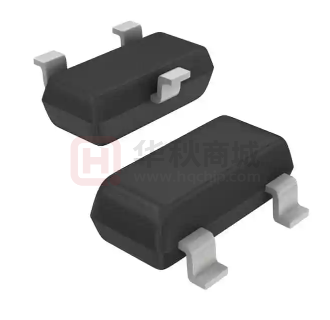
SOT-23 (DBZ) small, standard, common footprint
SOT-323, SC-70 (DCK) very small, standard,
space saving, common footprint
Leaded packages used for automatic optical
inspection (AOI)
This device features a low IO capacitance per
channel and a pin-out to suit two automotive CAN
bus lines (CANH and CANL) from the damage
caused by ElectroStatic Discharge (ESD) and other
transients. Additionally, the 3 pF (typical) or less line
capacitance of the ESD2CANxx24-Q1 is suitable for
CAN, CANFD, CAN SiC, and CAN-XL applications
that can support data rates up to 10 Mbps.
The ESD2CANxx24-Q1 is offered in two leaded
packages for easy flow through routing.
2 Applications
•
•
Automotive in-vehicle networks:
– Controller area network (CAN)
– Controlled area network flexible data-rate
(CAN-FD)
– Low, fault tolerant CAN
– High-speed CAN
Industrial control networks:
– DeviceNet IEC 62026-3
– CANopen – CiA 301/302-2 and EN 50325-4
Package Information(1)
PART NUMBER
PACKAGE
ESD2CAN24-Q1
BODY SIZE (NOM)
DBZ (SOT-23, 3)
2.92 mm × 1.30 mm
DCK (SC-70, 3)
2.00 mm × 1.25 mm
ESD2CANFD24-Q1
DBZ (SOT-23, 3)
2.92 mm × 1.30 mm
ESD2CANXL24-Q1
DBZ (SOT-23, 3)
2.92 mm × 1.30 mm
(1)
For all available packages, see the orderable addendum at
the end of the data sheet.
CANH
TXD
Application
(for example,
MCU I/O)
RT/2
CAN
Bus
CAN
TRANSCEIVER
RT/2
RXD
CANL
CG
1
2
ESD2CANxx24-Q1
3
ESD2CANxx24-Q1 Typical Application
An IMPORTANT NOTICE at the end of this data sheet addresses availability, warranty, changes, use in safety-critical applications,
intellectual property matters and other important disclaimers. UNLESS OTHERWISE NOTED, this document contains PRODUCTION
DATA.
�ESD2CAN24-Q1, ESD2CANFD24-Q1, ESD2CANXL24-Q1
www.ti.com
SLVSFW5C – APRIL 2022 – REVISED NOVEMBER 2022
Table of Contents
1 Features............................................................................1
2 Applications..................................................................... 1
3 Description.......................................................................1
4 Revision History.............................................................. 2
5 Pin Configuration and Functions...................................3
6 Specifications.................................................................. 4
6.1 Absolute Maximum Ratings........................................ 4
6.2 ESD Ratings—AEC Specification............................... 4
6.3 ESD Ratings—IEC Specification................................ 4
6.4 ESD Ratings - ISO Specification.................................5
6.5 Recommended Operating Conditions.........................5
6.6 Thermal Information....................................................5
6.7 Electrical Characteristics.............................................5
6.8 Typical Characteristics – ESD2CAN24-Q1................. 7
6.9 Typical Characteristics – ESD2CANFD24-Q1............ 9
7 Detailed Description...................................................... 11
7.1 Overview................................................................... 11
7.2 Functional Block Diagram......................................... 11
7.3 Feature Description...................................................11
7.4 Device Functional Modes..........................................12
8 Application and Implementation.................................. 13
8.1 Application Information............................................. 13
8.2 Typical Application.................................................... 13
9 Power Supply Recommendations................................14
10 Layout...........................................................................15
10.1 Layout Guidelines................................................... 15
10.2 Layout Example...................................................... 15
11 Device and Documentation Support..........................16
11.1 Documentation Support.......................................... 16
11.2 Receiving Notification of Documentation Updates.. 16
11.3 Support Resources................................................. 16
11.4 Trademarks............................................................. 16
11.5 Electrostatic Discharge Caution.............................. 16
11.6 Glossary.................................................................. 16
12 Mechanical, Packaging, and Orderable
Information.................................................................... 16
4 Revision History
NOTE: Page numbers for previous revisions may differ from page numbers in the current version.
Changes from Revision B (September 2022) to Revision C (November 2022)
Page
• Changed the status of the ESD2CANFD24-Q1 and ESD2CANXL24-Q1 devices from: preview to: active ...... 1
• Added the Application Curves section.............................................................................................................. 14
Changes from Revision A (June 2022) to Revision B (September 2022)
Page
• Changed the status of data sheet from: Advanced Information to: Production Data .........................................1
2
Submit Document Feedback
Copyright © 2022 Texas Instruments Incorporated
Product Folder Links: ESD2CAN24-Q1 ESD2CANFD24-Q1 ESD2CANXL24-Q1
�ESD2CAN24-Q1, ESD2CANFD24-Q1, ESD2CANXL24-Q1
www.ti.com
SLVSFW5C – APRIL 2022 – REVISED NOVEMBER 2022
5 Pin Configuration and Functions
IO
1
3
IO
GND
2
Not to scale
Figure 5-1. DCK or DBZ Package, 3-Pin SC-70 or SOT-23 (Top View)
Table 5-1. Pin Functions
PIN
TYPE(1)
DESCRIPTION
NAME
NO.
IO
1, 2
I/O
ESD protected IO
3
G
Connect to ground.
GND
(1)
I = Input, O = Output, I/O = Input or Output, G = Ground, P = Power
Copyright © 2022 Texas Instruments Incorporated
Submit Document Feedback
Product Folder Links: ESD2CAN24-Q1 ESD2CANFD24-Q1 ESD2CANXL24-Q1
3
�ESD2CAN24-Q1, ESD2CANFD24-Q1, ESD2CANXL24-Q1
www.ti.com
SLVSFW5C – APRIL 2022 – REVISED NOVEMBER 2022
6 Specifications
6.1 Absolute Maximum Ratings
over operating free-air temperature range (unless otherwise noted)(1)
Parameter
PPP
DEVICE
IEC 61000-4-5 Power (tp – 8/20 µs) at 25°C
IPP
IEC 61000-4-5 current (tp – 8/20 µs) at 25°C
MIN
MAX
ESD2CAN24-Q1
210
ESD2CANFD24-Q1
133
ESD2CANXL24-Q1
90
ESD2CAN24-Q1
5.7
ESD2CANFD24-Q1
3.5
ESD2CANXL24-Q1
2.5
TA
Operating free-air temperature
-55
150
TJ
Junction temperature
-55
150
Tstg
Storage temperature
-65
155
(1)
UNIT
W
A
°C
Operation outside the Absolute Maximum Ratings may cause permanent device damage. Absolute Maximum Ratings do not imply
functional operation of the device at these or any other conditions beyond those listed under Recommended Operating Conditions.
If used outside the Recommended Operating Conditions but within the Absolute Maximum Ratings, the device may not be fully
functional, and this may affect device reliability, functionality, performance, and shorten the device lifetime.
6.2 ESD Ratings—AEC Specification
Parameter
V(ESD)
(1)
(2)
Test Conditions
VALUE
Human body model (HBM), per AEC Q101-001
Electrostatic discharge
(1)
Charged device model (CDM), per AEC Q101-005 (2)
± 2500
± 1000
UNIT
V
JEDEC document JEP155 states that 500-V HBM allows safe manufactuuring with a standard ESD control proccess.
JEDEC document JEP157 states that 250-V CDM allows safe manufactuuring with a standard ESD control proccess.
6.3 ESD Ratings—IEC Specification
over TA = 25°C (unless otherwise noted)
Parameter
Test Conditions
IEC 61000-4-2 Contact Discharge, all pins
V(ESD)
Electrostatic discharge
IEC 61000-4-2 Air-gap Discharge, all pins
4
Submit Document Feedback
DEVICE
VALUE
ESD2CAN24-Q1
±30000
ESD2CANFD24-Q1
±25000
ESD2CANXL24-Q1
±20000
ESD2CAN24-Q1
±30000
ESD2CANFD24-Q1
±25000
ESD2CANXL24-Q1
±20000
UNIT
V
Copyright © 2022 Texas Instruments Incorporated
Product Folder Links: ESD2CAN24-Q1 ESD2CANFD24-Q1 ESD2CANXL24-Q1
�ESD2CAN24-Q1, ESD2CANFD24-Q1, ESD2CANXL24-Q1
www.ti.com
SLVSFW5C – APRIL 2022 – REVISED NOVEMBER 2022
6.4 ESD Ratings - ISO Specification
over TA = 25°C (unless otherwise noted)
Parameter
Test Conditions
DEVICE
ISO 10605, 150-pF, 330-Ω, IO
Contact discharge
ISO 10605, 330-pF, 330-Ω, IO
V(ESD)
Electrostatic discharge
ISO 10605, 150-pF, 330-Ω, IO
Air-gap discharge
ISO 10605, 330-pF, 330-Ω, IO
VALUE
ESD2CAN24-Q1
±30000
ESD2CANFD24-Q1
±25000
ESD2CANXL24-Q1
±20000
ESD2CAN24-Q1
±30000
ESD2CANFD24-Q1
±25000
ESD2CANXL24-Q1
±20000
ESD2CAN24-Q1
±30000
ESD2CANFD24-Q1
±25000
ESD2CANXL24-Q1
±20000
ESD2CAN24-Q1
±30000
ESD2CANFD24-Q1
±25000
ESD2CANXL24-Q1
±20000
UNIT
V
6.5 Recommended Operating Conditions
over operating free-air temperature range (unless otherwise noted)
Parameter
MIN
NOM
MAX
UNIT
VIN
Input voltage
-24
24
V
TA
Operating free-air temperature
-55
150
°C
6.6 Thermal Information
ESD2CAN24-Q1
THERMAL METRIC(1)
ESD2CANFD24-Q1 ESD2CANXL24-Q1
DBZ (SOT-23)
DCK (SOT-323 / SC-70)
DBZ (SOT-23)
DBZ (SOT-23)
UNIT
3 PINS
3 PINS
3 PINS
3 PINS
Junction-to-ambient thermal
resistance
291.5
283.0
316.3
325.3
°C/W
Junction-to-case (top) thermal
resistance
147.1
164.1
170.7
178.8
°C/W
RθJB
Junction-to-board thermal
resistance
131.1
105.1
156.2
165.5
°C/W
ΨJT
Junction-to-top characterization
parameter
32.0
67.1
45.9
52.4
°C/W
ΨJB
Junction-to-board characterization
parameter
130.2
104.4
155.1
164.4
°C/W
Junction-to-case (bottom) thermal
resistance
N/A
N/A
N/A
N/A
°C/W
RθJA
Rθ
JC(top)
Rθ
JC(bot)
(1)
For more information about traditional and new thermal metrics, see the Semiconductor and IC Package Thermal Metrics application
report.
6.7 Electrical Characteristics
over TA = 25°C (unless otherwise noted)(1)
PARAMETER
TEST CONDITIONS
VRWM
Reverse stand-off voltage
VBRF
Breakdown voltage(2)
VBRR
voltage(2)
Breakdown
DEVICE
MIN
TYP
MAX
UNIT
–24
24
V
IIO = 10 mA, IO to GND
25.5
35.5
V
IIO = –10 mA, IO to GND
–35.5
–25.5
V
Copyright © 2022 Texas Instruments Incorporated
Submit Document Feedback
Product Folder Links: ESD2CAN24-Q1 ESD2CANFD24-Q1 ESD2CANXL24-Q1
5
�ESD2CAN24-Q1, ESD2CANFD24-Q1, ESD2CANXL24-Q1
www.ti.com
SLVSFW5C – APRIL 2022 – REVISED NOVEMBER 2022
over TA = 25°C (unless otherwise noted)(1)
PARAMETER
TEST CONDITIONS
VCLAMP Clamping voltage(3)
VCLAMP Clamping voltage(4)
DEVICE
MIN
ESD2CAN24-Q1
37
IPP = 3.5 A, tp = 8/20 µs, IO to GND
ESD2CANFD24-Q1
37
IPP = 2.5 A, tp = 8/20 µs, IO to GND
ESD2CANXL24-Q1
36
ESD2CAN24-Q1
35
ESD2CANFD24-Q1
36
ESD2CANXL24-Q1
38
ESD2CAN24-Q1
30
ESD2CANFD24-Q1
30
IPP = 16 A, TLP, IO to GND or GND to IO
VHold
Holding voltage after
snapback
TLP
ILEAK
Leakage current
VIO = ±24 V, IO to GND
RDYN
Dynamic resistance(4)
IO to GND and GND to IO
ESD2CANXL24-Q1
(1)
(2)
(3)
(4)
(5)
6
Line capacitance(5)
VIO = 0 V, f = 1 MHz, Vpp = 30 mV
MAX
UNIT
V
V
V
30
-50
5
50
nA
ESD2CAN24-Q1
0.35
Ω
ESD2CANFD24-Q1
0.45
Ω
ESD2CANXL24-Q1
0.57
ESD2CAN24-Q1
CL
TYP
IPP = 5.7 A, tp = 8/20 µs, IO to GND
Ω
3
5
ESD2CANFD24-Q1
2.5
4.2
ESD2CANXL24-Q1
1.7
2.8
pF
Measurements made on each IO channel
VBRF and VBRR are defined as the voltage when ±10 mA is applied in the positive and negative going direction respectively, before the
device latches into the snapback state
Device stressed with 8/20 μs exponential decay waveform according to IEC 61000-4-5
Non-repetitive current pulse, Transmission Line Pulse (TLP); square pulse; ANSI / ESD STM5.5.1-2008
Measured from IO to GND on each channel
Submit Document Feedback
Copyright © 2022 Texas Instruments Incorporated
Product Folder Links: ESD2CAN24-Q1 ESD2CANFD24-Q1 ESD2CANXL24-Q1
�ESD2CAN24-Q1, ESD2CANFD24-Q1, ESD2CANXL24-Q1
www.ti.com
SLVSFW5C – APRIL 2022 – REVISED NOVEMBER 2022
28
26
24
22
20
18
16
14
12
10
8
6
4
2
0
Ipp (A)
Ipp (A)
6.8 Typical Characteristics – ESD2CAN24-Q1
5
10
15
20
25
Vclamp (V)
30
35
40
28
26
24
22
20
18
16
14
12
10
8
6
4
2
0
5
10
Figure 6-1. Positive TLP Curve
30
35
40
Figure 6-2. Negative TLP Curve
150
25
125
0
-25
Voltage (V)
100
Voltage (V)
20
25
Vclamp (V)
tp = 100 ns, Transmission Line Pulse (TLP)
tp = 100 ns, Transmission Line Pulse (TLP)
75
50
Vclamp_ESD at 30ns = 28V
25
Vclamp_ESD at 30ns = -32.9V
-50
-75
-100
-125
0
-150
-25
-100
0
100
200
300
400
Time(ns)
500
600
-175
-100
700
Figure 6-3. +8-kV Clamped IEC Waveform
0
100
200
300
400
Time(ns)
500
600
700
Figure 6-4. −8-kV Clamped IEC Waveform
3.2
10
3.1
8
6
3
4
2.9
ILEAK (nA)
Capacitance (pF)
15
2.8
2.7
2
0
-2
2.6
-4
2.5
-6
-8
2.4
2.3
-10
-25
Frequency = 1MHz, V pp = 30 mV
2.2
0
0.2
0.4
0.6
0.8
1
1.2
VR (V)
1.4
1.6
1.8
Figure 6-5. Capacitance vs. Bias Voltage
Copyright © 2022 Texas Instruments Incorporated
2
-20
-15
-10
-5
0
VR (V)
5
10
15
20
25
TA = 150 C
ILEAK is less than 1 nA at -55 C and 25 C.
Figure 6-6. Leakage Current vs. Bias Voltage Across
Temperature
Submit Document Feedback
Product Folder Links: ESD2CAN24-Q1 ESD2CANFD24-Q1 ESD2CANXL24-Q1
7
�ESD2CAN24-Q1, ESD2CANFD24-Q1, ESD2CANXL24-Q1
www.ti.com
SLVSFW5C – APRIL 2022 – REVISED NOVEMBER 2022
6
5
60
Current 55
Voltage
50
4.5
45
Current (A)
5.5
4
40
3.5
35
3
30
2.5
25
2
20
1.5
15
1
10
0.5
0
-5
Voltage (V)
6.8 Typical Characteristics – ESD2CAN24-Q1 (continued)
5
0
5
10
15
20
Time ( s)
25
30
35
0
40
Figure 6-7. 8/20 μs Surge Response at 5.7 A
8
Submit Document Feedback
Copyright © 2022 Texas Instruments Incorporated
Product Folder Links: ESD2CAN24-Q1 ESD2CANFD24-Q1 ESD2CANXL24-Q1
�ESD2CAN24-Q1, ESD2CANFD24-Q1, ESD2CANXL24-Q1
www.ti.com
SLVSFW5C – APRIL 2022 – REVISED NOVEMBER 2022
30
30
27
27
24
24
21
21
18
18
Ipp (A)
Ipp (A)
6.9 Typical Characteristics – ESD2CANFD24-Q1
15
12
15
12
9
9
6
6
3
3
0
0
-3
-3
0
5
10
15
20
25
Vclamp (V)
30
35
40
45
0
5
10
15
20
25
Vclamp (V)
30
35
40
45
tp = 100 ns, Transmission Line Pulse (TLP)
tp = 100 ns, Transmission Line Pulse (TLP)
Figure 6-9. Negative TLP Curve
Figure 6-8. Positive TLP Curve
175
150
Voltage (V)
125
100
75
Vclamp_ESD at 30ns = 27.3V
50
25
0
-25
-100
0
100
200
300
400
Time(ns)
500
600
700
2.3
2.28
2.26
2.24
2.22
2.2
2.18
2.16
2.14
2.12
2.1
2.08
2.06
2.04
2.02
2
-25
Figure 6-11. −8-kV Clamped IEC Waveform
10
8
6
4
ILEAK (nA)
Capacitance (pF)
Figure 6-10. +8-kV Clamped IEC Waveform
2
0
-2
-4
-6
-8
-10
-25
-20
-15
-10
-5
0
VR (V)
5
10
15
20
Figure 6-12. Capacitance vs. Bias Voltage
Copyright © 2022 Texas Instruments Incorporated
25
-20
-15
-10
-5
0
VR (V)
5
10
15
20
25
TA = 150 C
ILEAK is less than 1 nA at -55 C and 25 C.
Figure 6-13. Leakage Current vs. Bias Voltage Across
Temperature
Submit Document Feedback
Product Folder Links: ESD2CAN24-Q1 ESD2CANFD24-Q1 ESD2CANXL24-Q1
9
�ESD2CAN24-Q1, ESD2CANFD24-Q1, ESD2CANXL24-Q1
www.ti.com
SLVSFW5C – APRIL 2022 – REVISED NOVEMBER 2022
Voltage (V)
40
36
4
Voltage (V)
Current (A) 3.6
32
3.2
28
2.8
24
2.4
20
2
16
1.6
12
1.2
8
0.8
4
0.4
0
-5
0
5
10
15
20
25
Time ( s)
30
35
40
Current (A)
6.9 Typical Characteristics – ESD2CANFD24-Q1 (continued)
0
45
Figure 6-14. 8/20 μs Surge Response at 5.7 A
10
Submit Document Feedback
Copyright © 2022 Texas Instruments Incorporated
Product Folder Links: ESD2CAN24-Q1 ESD2CANFD24-Q1 ESD2CANXL24-Q1
�ESD2CAN24-Q1, ESD2CANFD24-Q1, ESD2CANXL24-Q1
www.ti.com
SLVSFW5C – APRIL 2022 – REVISED NOVEMBER 2022
7 Detailed Description
7.1 Overview
The ESD2CANxx24-Q1 is a dual-channel ESD TVS diode in SOT-23 and SC-70 leaded packages which are
convenient for automatic optical inspection. This product offers ISO 10605 ±30-kV or ±25-kV or ±20-kV air-gap,
±30-kV or ±25-kV or ±20-kV contact ESD protection, and has a clamp circuit with a back-to-back TVS diode for
bidirectional signal support. The 3 pF (typical) or less line capacitance of this ESD protection diode is suitable for
CAN, CANFD, CAN SiC, and CAN-XL applications that can support data rates up to 10 Mbps.
A typical application for this product is ESD circuit protection for CAN transceivers used in automotive
applications. The ESD2CANxx24-Q1 is a good fit for the ESD protection inside automotive electronic control
units (ECUs) for head lights, door modules, climate control, roof control, wipers, cluster, audio, and many other
automotive applications.
7.2 Functional Block Diagram
1
2
3
7.3 Feature Description
The ESD2CANxx24-Q1 is a bidirectional TVS with a high ESD protection level. This device protects the circuit
from ESD strikes up to ±30-kV or ±25-kV or ±20-kV contact and ±30-kV or ±25-kV or ±20-kV air-gap specified
in the ISO 10605 automotive standard. The device can also handle up to 5.7 A surge current (IEC 61000-4-5
8/20 µs). The I/O capacitance of 3-pF (typical) supports a data rate up to 10 Mbps. This clamping device has
a small dynamic resistance, which makes the clamping voltage low when the device is actively protecting other
circuits. For example, the clamping voltage is only 37 V when the device is taking 5.7 A transient surge current.
The breakdown is bidirectional so this protection device is a good fit for CAN which is a differential signal. Low
leakage allows the diode to conserve power when working below the VRWM. The temperature range of −55°C to
+150°C makes this ESD device work at extensive temperatures in most environments. The leaded SOT-23 and
SC-70 packages are good for applications requiring automatic optical inspection (AOI).
7.3.1 AEC-Q101 Qualified and Temperature Range
This device is qualified to AEC-Q101 standards and is qualified to operate from –55°C to +150°C.
7.3.2 ISO 10605 ESD Protection
The I/O pins can withstand ESD events of at least ±30-kV contact and ±30-kV air-gap in the leaded SOT-23 and
SC-70 packages according to the ISO 10605 (330 pF and 330 Ω loading condition) standard. An ESD-surge
clamp diverts the current to ground.
7.3.3 IEC 61000-4-5 Surge Protection
The IO pins can withstand surge events up to 5.7 A (8/20 µs waveform). An ESD-surge clamp diverts this
current to ground.
7.3.4 IO Capacitance
The capacitance between the I/O pins is 3 pF (typical) or less. This capacitance supports data rates for CAN,
CANFD, CAN SiC, and CAN-XL up to 10 Mbps.
Copyright © 2022 Texas Instruments Incorporated
Submit Document Feedback
Product Folder Links: ESD2CAN24-Q1 ESD2CANFD24-Q1 ESD2CANXL24-Q1
11
�ESD2CAN24-Q1, ESD2CANFD24-Q1, ESD2CANXL24-Q1
www.ti.com
SLVSFW5C – APRIL 2022 – REVISED NOVEMBER 2022
7.3.5 Dynamic Resistance
The IO pins feature an ESD clamp that has a low RDYN of 0.57 Ω (Pin 1 or Pin 2 to Pin 3) and 0.57 Ω (Pin 3 to
Pin 1 or Pin 2) or less which prevents system damage during ESD events.
7.3.6 DC Breakdown Voltage
The DC breakdown voltage between the IO pins is a minimum of ± 25.5 V. This protects sensitive equipment
from surges above the reverse standoff voltage of ± 24 V.
7.3.7 Ultra Low Leakage Current
The IO pins feature an ultra-low leakage current of ± 50 nA (maximum) with a bias of ± 24 V.
7.3.8 Clamping Voltage
The IO pins feature an ESD clamp that is capable of clamping the voltage to 37 V (IPP = 5.7 A) and 35 V (IPP =
16 A for TLP) for ESD2CAN24-Q1, and 38 V (IPP = 3.5 A) and 34 V (IPP = 16 A for TLP) for ESD2CANFD24-Q1,
and 36 V (IPP = 1.5 A) and 38 V (IPP = 16 A for TLP) for ESD2CANXL24-Q1.
7.3.9 Industry Standard Leaded Packages
This device features industry standard SOT-23 (DBZ) and SC-70 (DCK) leaded packages for automatic optical
inspection (AOI).
7.4 Device Functional Modes
The ESD2CANxx24-Q1 is a dual channel passive clamp that has low leakage during normal operation when the
voltage between pin 1 or pin 2 and pin 3 is below VRWM, and activates when the voltage between pin 1 or pin 2
and pin 3 goes above VBR. During ISO 10605 ESD events, transient voltages as high as ±30 kV can be clamped
on either channel. When the voltages on the protected lines fall below the VHOLD, the device reverts back to the
low leakage passive state.
12
Submit Document Feedback
Copyright © 2022 Texas Instruments Incorporated
Product Folder Links: ESD2CAN24-Q1 ESD2CANFD24-Q1 ESD2CANXL24-Q1
�ESD2CAN24-Q1, ESD2CANFD24-Q1, ESD2CANXL24-Q1
www.ti.com
SLVSFW5C – APRIL 2022 – REVISED NOVEMBER 2022
8 Application and Implementation
Note
Information in the following applications sections is not part of the TI component specification,
and TI does not warrant its accuracy or completeness. TI’s customers are responsible for
determining suitability of components for their purposes, as well as validating and testing their design
implementation to confirm system functionality.
8.1 Application Information
The ESD2CANxx24-Q1 is a dual channel TVS diode which is used to provide a path to ground for dissipating
ESD events on differential CAN signal lines. The CAN signal lines are typically routed throughout the automobile
to connect between the different ECUs. As the current from ESD passes through the TVS, only a small voltage
drop is present across the diode. This is the voltage presented to the protected IC. The low RDYN of the triggered
TVS holds this voltage, VCLAMP, to a safe level for the protected IC.
8.2 Typical Application
CANH
TXD
Application
(for example,
MCU I/O)
RT/2
CAN
Bus
CAN
TRANSCEIVER
RT/2
RXD
CANL
CG
1
2
ESD2CANxx24-Q1
3
Figure 8-1. ESD2CANxx24-Q1 Typical Application
8.2.1 Design Requirements
For this design example, the ESD2CANxx24-Q1 is used to provide ESD protection for a CAN transceiver. Table
8-1 lists the known design parameters for this application.
Table 8-1. Design Parameters for the ESD2CAN24-Q1 Typical Application
Design Parameter
Value
Diode configuration
Bidirectional
VIO differential signal range
> ±1.5 V
VRWM
±24 V
Jumpstart short to battery event on VIO
±24 V
Data rate
Up to 10 Mbps
RT/2
60 Ω
Copyright © 2022 Texas Instruments Incorporated
Submit Document Feedback
Product Folder Links: ESD2CAN24-Q1 ESD2CANFD24-Q1 ESD2CANXL24-Q1
13
�ESD2CAN24-Q1, ESD2CANFD24-Q1, ESD2CANXL24-Q1
www.ti.com
SLVSFW5C – APRIL 2022 – REVISED NOVEMBER 2022
8.2.2 Detailed Design Procedure
The ESD2CANxx24-Q1 has a VRWM of ±24 V to protect the diode from being damaged during a short to battery
event that can occur by reversing the terminal connections during jumpstart. The bidirectional characteristic
enables the signal integrity of the differential CAN lines to not be impacted by the diode. The low capacitance
of 3 pF (typical) or less enables data rates up to 10 Mbps, which allows the designer to meet the requirements
for CAN, CANFD, CAN SiC, and CAN-XL. The 60 Ω split termination improves the electromagnetic emissions
behavior of the network by filtering higher-frequency common-mode noise that may be present on the differential
signal lines.
8.2.3 Application Curves
25
150
0
125
-25
Voltage (V)
75
50
Vclamp_ESD at 30ns = 28V
25
-75
-100
-125
0
-25
-100
Vclamp_ESD at 30ns = -32.9V
-50
-150
0
100
200
300
400
Time(ns)
500
600
-175
-100
700
Figure 8-2. +8-kV Clamped IEC Waveform
100
6
5
60
Current 55
Voltage
50
4.5
45
4
40
3.5
35
3
30
2.5
25
2
20
1.5
15
1
300
400
Time(ns)
500
600
700
10
0.5
0
-5
200
Figure 8-3. −8-kV Clamped IEC Waveform
5.5
Current (A)
0
Voltage (V)
Voltage (V)
100
5
0
5
10
15
20
Time ( s)
25
30
35
0
40
Figure 8-4. 8/20 µs Surge Response at 5.7 A
9 Power Supply Recommendations
This device is a passive TVS diode-based ESD protection device, therefore there is no requirement to power it.
Ensure that the maximum voltage specifications for each pin are not violated.
14
Submit Document Feedback
Copyright © 2022 Texas Instruments Incorporated
Product Folder Links: ESD2CAN24-Q1 ESD2CANFD24-Q1 ESD2CANXL24-Q1
�ESD2CAN24-Q1, ESD2CANFD24-Q1, ESD2CANXL24-Q1
www.ti.com
SLVSFW5C – APRIL 2022 – REVISED NOVEMBER 2022
10 Layout
10.1 Layout Guidelines
•
•
•
•
The optimum placement of the device is as close to the connector as possible.
– EMI during an ESD event can couple from the trace being struck to other nearby unprotected traces,
resulting in early system failures.
– The PCB designer must minimize the possibility of EMI coupling by keeping any unprotected traces away
from the protected traces which are between the TVS and the connector.
Route the protected traces as straight as possible.
Eliminate any sharp corners on the protected traces between the TVS and the connector by using rounded
corners with the largest radii possible.
– Electric fields tend to build up on corners, increasing EMI coupling.
If pin 3 is connected to ground, use a thick and short trace for this return path.
10.2 Layout Example
This example is typical of a dual channel differential data pair application, such as CAN.
IO1
GND
IO2
= VIA to GND
Figure 10-1. Routing with DBZ and DCK Package
Copyright © 2022 Texas Instruments Incorporated
Submit Document Feedback
Product Folder Links: ESD2CAN24-Q1 ESD2CANFD24-Q1 ESD2CANXL24-Q1
15
�ESD2CAN24-Q1, ESD2CANFD24-Q1, ESD2CANXL24-Q1
www.ti.com
SLVSFW5C – APRIL 2022 – REVISED NOVEMBER 2022
11 Device and Documentation Support
TI offers an extensive line of development tools. Tools and software to evaluate the performance of the device,
generate code, and develop solutions are listed below.
11.1 Documentation Support
11.1.1 Related Documentation
For related documentation, see the following:
•
•
•
•
Texas Instruments, ESD Layout Guide user's guide
Texas Instruments, ESD Protection Diodes EVM user's guide
Texas Instruments, Generic ESD Evaluation Module user's guide
Texas Instruments, Reading and Understanding an ESD Protection data sheet
11.2 Receiving Notification of Documentation Updates
To receive notification of documentation updates, navigate to the device product folder on ti.com. Click on
Subscribe to updates to register and receive a weekly digest of any product information that has changed. For
change details, review the revision history included in any revised document.
11.3 Support Resources
TI E2E™ support forums are an engineer's go-to source for fast, verified answers and design help — straight
from the experts. Search existing answers or ask your own question to get the quick design help you need.
Linked content is provided "AS IS" by the respective contributors. They do not constitute TI specifications and do
not necessarily reflect TI's views; see TI's Terms of Use.
11.4 Trademarks
TI E2E™ is a trademark of Texas Instruments.
All trademarks are the property of their respective owners.
11.5 Electrostatic Discharge Caution
This integrated circuit can be damaged by ESD. Texas Instruments recommends that all integrated circuits be handled
with appropriate precautions. Failure to observe proper handling and installation procedures can cause damage.
ESD damage can range from subtle performance degradation to complete device failure. Precision integrated circuits may
be more susceptible to damage because very small parametric changes could cause the device not to meet its published
specifications.
11.6 Glossary
TI Glossary
This glossary lists and explains terms, acronyms, and definitions.
12 Mechanical, Packaging, and Orderable Information
The following pages include mechanical, packaging, and orderable information. This information is the most
current data available for the designated devices. This data is subject to change without notice and revision of
this document. For browser-based versions of this data sheet, refer to the left-hand navigation.
16
Submit Document Feedback
Copyright © 2022 Texas Instruments Incorporated
Product Folder Links: ESD2CAN24-Q1 ESD2CANFD24-Q1 ESD2CANXL24-Q1
�PACKAGE OPTION ADDENDUM
www.ti.com
2-Dec-2022
PACKAGING INFORMATION
Orderable Device
Status
(1)
Package Type Package Pins Package
Drawing
Qty
Eco Plan
(2)
Lead finish/
Ball material
MSL Peak Temp
Op Temp (°C)
Device Marking
(3)
Samples
(4/5)
(6)
ESD2CAN24DBZRQ1
ACTIVE
SOT-23
DBZ
3
3000
RoHS & Green
NIPDAU
Level-1-260C-UNLIM
-55 to 150
1L3
Samples
ESD2CAN24DCKRQ1
ACTIVE
SC70
DCK
3
3000
RoHS & Green
NIPDAU
Level-3-260C-168 HR
-55 to 150
1L6
Samples
ESD2CANFD24DBZRQ1
ACTIVE
SOT-23
DBZ
3
3000
RoHS & Green
NIPDAU
Level-1-260C-UNLIM
-50 to 150
2QP8
Samples
ESD2CANXL24DBZRQ1
ACTIVE
SOT-23
DBZ
3
3000
RoHS & Green
NIPDAU
Level-1-260C-UNLIM
-50 to 150
2RI8
Samples
(1)
The marketing status values are defined as follows:
ACTIVE: Product device recommended for new designs.
LIFEBUY: TI has announced that the device will be discontinued, and a lifetime-buy period is in effect.
NRND: Not recommended for new designs. Device is in production to support existing customers, but TI does not recommend using this part in a new design.
PREVIEW: Device has been announced but is not in production. Samples may or may not be available.
OBSOLETE: TI has discontinued the production of the device.
(2)
RoHS: TI defines "RoHS" to mean semiconductor products that are compliant with the current EU RoHS requirements for all 10 RoHS substances, including the requirement that RoHS substance
do not exceed 0.1% by weight in homogeneous materials. Where designed to be soldered at high temperatures, "RoHS" products are suitable for use in specified lead-free processes. TI may
reference these types of products as "Pb-Free".
RoHS Exempt: TI defines "RoHS Exempt" to mean products that contain lead but are compliant with EU RoHS pursuant to a specific EU RoHS exemption.
Green: TI defines "Green" to mean the content of Chlorine (Cl) and Bromine (Br) based flame retardants meet JS709B low halogen requirements of


 工商网监
湘ICP备2023018690号
工商网监
湘ICP备2023018690号
