Sample &
Buy
Product
Folder
Support &
Community
Tools &
Software
Technical
Documents
Reference
Design
FDC1004
SNOSCY5B – AUGUST 2014 – REVISED APRIL 2015
FDC1004 4-Channel Capacitance-to-Digital Converter for Capacitive Sensing Solutions
1 Features
3 Description
•
•
•
•
•
•
•
•
Capacitive sensing with grounded capacitor sensors
is a very low-power, low-cost, high-resolution contactless sensing technique that can be applied to a
variety of applications ranging from proximity sensing
and gesture recognition to material analysis and
remote liquid level sensing. The sensor in a
capacitive sensing system is any metal or conductor,
allowing for low cost and highly flexible system
design.
1
•
•
Input Range: ±15 pF
Measurement Resolution: 0.5 fF
Maximum Offset Capacitance: 100 pF
Programmable Output Rates: 100/200/400 S/s
Maximum Shield Load: 400 pF
Supply Voltage: 3.3 V
Temp Range: –40° to 125°C
Current Consumption:
– Active: 750 µA
– Standby: 29 µA
Interface: I2C
Number of Channels: 4
The FDC1004 is a high-resolution, 4-channel
capacitance-to-digital converter for implementing
capacitive sensing solutions. Each channel has a full
scale range of ±15 pF and can handle a sensor offset
capacitance of up to 100 pF, which can be either
programmed internally or can be an external
capacitor for tracking environmental changes over
time and temperature. The large offset capacitance
capability allows for the use of remote sensors.
2 Applications
•
•
•
•
•
•
•
•
•
Proximity Sensor
Gesture Recognition
Automotive Door / Kick Sensors
Automotive Rain Sensor
Remote and Direct Liquid Level Sensor
High-resolution Metal Profiling
Rain / Fog / Ice / Snow Sensor
Material Size Detection
Material Stack Height
The FDC1004 also includes shield drivers for sensor
shields, which can reduce EMI interference and help
focus the sensing direction of a capacitive sensor.
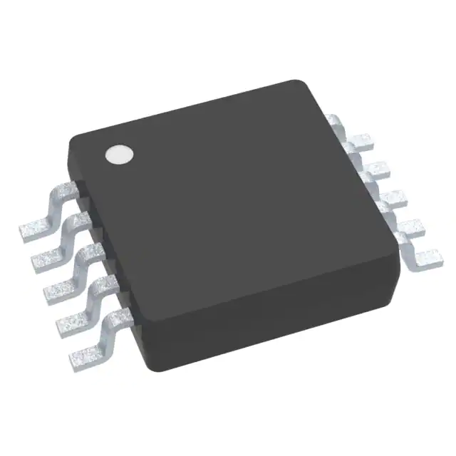
The small footprint of the FDC1004 allows for use in
space-constrained applications. The FDC1004 is
available in a 10-pin WSON and VSSOP package
and features an I2C interface for interfacing to an
MCU.
Device Information(1)
PART NUMBER
FDC1004
PACKAGE
BODY SIZE (NOM)
WSON (DSC)
3.0 mm x 3.0 mm
VSSOP (DGS)
3.0 mm x 3.0 mm
(1) For all available packages, see the orderable addendum at
the end of the datasheet.
4 Typical Application
3.3 V
LEVEL
SENSOR
VDD
SHLD1
ENVIRONMENTAL
SENSOR
EXCITATION
SHLD2
3.3 V 3.3 V
CIN1
FDC1004
3.3 V
CIN2
CIN3
CHA
MUX
CHA
CIN4
CAPACITANCE
TO DIGITAL
CONVERTER
LIQUID
SENSOR
CHB
MUX
VDD
OFFSET
& GAIN
CALIBRATION
MCU
SCL
CHB
CONFIGURATION & DATA
REGISTERS
I2C
SDA
I2C
Peripheral
GND
CAPDAC
GND
1
An IMPORTANT NOTICE at the end of this data sheet addresses availability, warranty, changes, use in safety-critical applications,
intellectual property matters and other important disclaimers. PRODUCTION DATA.
�FDC1004
SNOSCY5B – AUGUST 2014 – REVISED APRIL 2015
www.ti.com
Table of Contents
1
2
3
4
5
6
7
8
Features ..................................................................
Applications ...........................................................
Description .............................................................
Typical Application ................................................
Revision History.....................................................
Pin Configuration and Functions .........................
Specifications.........................................................
1
1
1
1
2
4
5
7.1
7.2
7.3
7.4
7.5
7.6
7.7
7.8
5
5
5
5
6
6
7
8
Absolute Maximum Ratings ......................................
ESD Ratings..............................................................
Recommended Operating Conditions.......................
Thermal Information .................................................
Electrical Characteristics...........................................
I2C Interface Voltage Level ......................................
I2C Interface Timing .................................................
Typical Characteristics ..............................................
Detailed Description ............................................ 10
8.1 Overview ................................................................. 10
8.2 Functional Block Diagram ....................................... 10
8.3 Feature Description................................................. 10
8.4 Device Functional Modes........................................ 11
8.5 Programming........................................................... 13
8.6 Register Maps ........................................................ 16
9
Applications and Implementation ...................... 20
9.1
9.2
9.3
9.4
Application Information............................................
Typical Application .................................................
Do's and Don'ts ......................................................
Initialization Set Up ................................................
20
21
23
23
10 Power Supply Recommendations ..................... 23
11 Layout................................................................... 23
11.1 Layout Guidelines ................................................. 23
11.2 Layout Example .................................................... 23
12 Device and Documentation Support ................. 24
12.1
12.2
12.3
12.4
Documentation Support .......................................
Trademarks ...........................................................
Electrostatic Discharge Caution ............................
Glossary ................................................................
24
24
24
24
13 Mechanical, Packaging, and Orderable
Information ........................................................... 24
5 Revision History
Changes from Revision A (October 2014) to Revision B
Page
•
Changed max temp range from 85C to 125C throughout ..................................................................................................... 1
•
Added VSSOP package type ................................................................................................................................................. 1
•
Added note to Electrical Characteristics table ....................................................................................................................... 2
•
Deleted WSON DAP explicit assignment to GND in diagram ................................................................................................ 4
•
Added VSSOP package diagram .......................................................................................................................................... 4
•
Changed table from Handling Ratings to ESD Ratings and moved Storage Temp to Absolute Maximum Ratings ............. 5
•
Added JA thermal resistance for VSSOP package ............................................................................................................... 5
•
Added JC thermal resistance for WSON package ................................................................................................................ 5
•
Added JC thermal resistance for VSSOP package ............................................................................................................... 5
•
Added JC thermal resistance for WSON package ................................................................................................................ 5
•
Added JB thermal resistance for VSSOP package ............................................................................................................... 5
•
Added note to Electrical Characteristics table ....................................................................................................................... 6
•
Added note to Electrical Characteristics limits ...................................................................................................................... 6
•
Changed TcCOFF to "46" from "30" ......................................................................................................................................... 6
•
Changed GERR to "0.2" from "0.07" ........................................................................................................................................ 6
•
Changed gain error unit to "%" from "% of full scale"............................................................................................................. 6
•
Changed tcG to "-37.5" from "2.1" ......................................................................................................................................... 6
•
Changed tcG unit to "ppm/°C" from "ppm of full scale/°C"..................................................................................................... 6
•
Added testing for PSRR condition .......................................................................................................................................... 6
•
Changed PSRR to "13.6" from "11" ...................................................................................................................................... 6
•
Changed FRCAPDACto "96.9" from "96.875" ............................................................................................................................ 6
•
Deleted CAPDAC resolution from EC table ........................................................................................................................... 6
•
Changed TcCOFFCAPDAC to "30" from "1" .............................................................................................................................. 6
•
Changed TcCOFFCAPDACto "fF" from "ppm of FS/°C" ............................................................................................................ 6
•
Changed DRV value of 400pF from typ and moved to max limit ........................................................................................... 6
2
Submit Documentation Feedback
Copyright © 2014–2015, Texas Instruments Incorporated
Product Folder Links: FDC1004
�FDC1004
www.ti.com
SNOSCY5B – AUGUST 2014 – REVISED APRIL 2015
Revision History (continued)
•
Changed plot for Active Supply Current vs Temperature due to change in temperature range ........................................... 8
•
Changed plot for Stand-by Supply Current vs Temperature due to change in temperature range ...................................... 8
•
Changed plot for Gain Drift vs Temperature due to change in temperature range and gain drift unit .................................. 8
•
Changed plot for Offset Drift vs Temperature due to change in temperature range ............................................................. 8
•
Added capacitance vs voltage plot ........................................................................................................................................ 8
•
Changed shield configuration example for differential mode from "CIN2-CIN1, where CHA=CIN2 and CHB=CIN1" to
"CIN1-CIN2, where CHA=CIN1 and CHB=CIN2" ................................................................................................................ 10
•
Changed shield configuration example for differential mode from "CIN2-CIN1, where CHA=CIN2 and CHB=CIN1" to
"CIN1-CIN2, where CHA=CIN1 and CHB=CIN2" ................................................................................................................ 12
•
Added note to Electrical Characteristics table ..................................................................................................................... 16
Changes from Original (August 2014) to Revision A
Page
•
Added Parameter not tested in production ............................................................................................................................ 6
•
Changed CINx to CINn throughout ..................................................................................................................................... 10
•
Added note for Applications and Implementation section. ................................................................................................... 20
Submit Documentation Feedback
Copyright © 2014–2015, Texas Instruments Incorporated
Product Folder Links: FDC1004
3
�FDC1004
SNOSCY5B – AUGUST 2014 – REVISED APRIL 2015
www.ti.com
6 Pin Configuration and Functions
WSON (DSC)
10 Pins
TOP
SHLD1
1
10
SDA
CIN1
2
9
SCL
CIN2
3
8
VDD
CIN3
4
7
GND
CIN4
5
6
SHLD2
DAP
VSSOP (DGS)
10 Pins
TOP
SHLD1
1
10
SDA
CIN1
2
9
SCL
CIN2
3
8
VDD
CIN3
4
7
GND
CIN4
5
6
SHLD2
Pin Functions
PIN
TYPE (1)
DESCRIPTION
NAME
NO.
SHLD1
1
A
Capacitive Input Active AC Shielding.
CIN1
2
A
Capacitive Input. The measured capacitance is connected between the CIN1 pin and GND. If
not used, this pin should be left as an open circuit.
CIN2
3
A
Capacitive Input. The measured capacitance is connected between the CIN2 pin and GND. If
not used, this pin should be left as an open circuit.
CIN3
4
A
Capacitive Input. The measured capacitance is connected between the CIN3 pin and GND. If
not used, this pin should be left as an open circuit.
CIN4
5
A
Capacitive Input. The measured capacitance is connected between the CIN4 pin and GND. If
not used, this pin should be left as an open circuit.
SHLD2
6
A
Capacitive Input Active AC Shielding.
GND
7
G
Ground
VDD
8
P
Power Supply Voltage. This pin should be decoupled to GND, using a low impedance
capacitor, for example in combination with a 1-μF tantalum and a 0.1-μF multilayer ceramic.
SCL
9
I
Serial Interface Clock Input. Connects to the master clock line. Requires pull-up resistor if not
already provided elsewhere in the system.
SDA
10
I/O
Serial Interface Bidirectional Data. Connects to the master data line. Requires a pull-up
resistor if not provided elsewhere in the system.
-
N/A
Connect to GND
DAP (2)
(1)
(2)
4
P=Power, G=Ground, I=Input, O=Output, A=Analog, I/O=Bi-Directional Input/Output
There is an internal electrical connection between the exposed Die Attach Pad (DAP) and the GND pin of the device. Although the DAP
can be left floating, for best performance the DAP should be connected to the same potential as the device's GND pin. Do not use the
DAP as the primary ground for the device. The device GND pin must always be connected to ground.
Submit Documentation Feedback
Copyright © 2014–2015, Texas Instruments Incorporated
Product Folder Links: FDC1004
�FDC1004
www.ti.com
SNOSCY5B – AUGUST 2014 – REVISED APRIL 2015
7 Specifications
7.1 Absolute Maximum Ratings (1)
Input voltage
Input current
MIN
MAX
UNIT
VDD
–0.3
6
V
SCL, SDA
–0.3
6
V
at any other pin
–0.3
VDD+0.3
V
3
mA
150
°C
150
°C
at any pin
Junction temperature (2)
Storage temperature
(1)
(2)
TSTG
–65
Stresses beyond those listed under Absolute Maximum Ratings may cause permanent damage to the device. These are stress ratings
only, which do not imply functional operation of the device at these or any other conditions beyond those indicated under Recommended
Operating Conditions. Exposure to absolute-maximum-rated conditions for extended periods may affect device reliability.
The maximum power dissipation is a function of TJ(MAX), RθJA, and the ambient temperature, TA. The maximum allowable power
dissipation at any ambient temperature is PDMAX = (TJ(MAX) - TA)/ RθJA. All numbers apply for packages soldered directly onto a PC
board.
7.2 ESD Ratings
VALUE
V(ESD)
(1)
(2)
(3)
Electrostatic discharge
(1)
Human body model (HBM), per ANSI/ESDA/JEDEC
JS-001, all pins (2)
±1000
Charged device model (CDM), per JEDEC
specification -500 500 JESD22-C101, all pins (3)
±250
UNIT
V
Electrostatic discharge (ESD) to measure device sensitivity and immunity to damage caused by assembly line electrostatic discharges in
to the device.
Level listed above is the passing level per ANSI, ESDA, and JEDEC JS-001. JEDEC document JEP155 states that 500-V HBM allows
safe manufacturing with a standard ESD control process.
Level listed above is the passing level per EIA-JEDEC JESD22-C101. JEDEC document JEP157 states that 250-V CDM allows safe
manufacturing with a standard ESD control process.
7.3 Recommended Operating Conditions
Over operating temperature range (unless otherwise noted)
MIN
NOM
MAX
3
3.3
3.6
V
125
°C
Supply voltage (VDD-GND)
Temperature
–40
UNIT
7.4 Thermal Information
FDC1004
THERMAL METRIC (1)
WSON (DSC)
VSSOP (DGS)
UNIT
10 PINS
RθJA
Junction-to-ambient thermal resistance
46.8
46.8
°C/W
RθJC
Junction-to-case(top) thermal resistance
46.7
48.7
°C/W
RθJB
Junction-to-board thermal resistance
21.5
70.6
°C/W
(1)
For more information about traditional and new thermal metrics, see the IC Package Thermal Metrics application report, SPRA953.
Submit Documentation Feedback
Copyright © 2014–2015, Texas Instruments Incorporated
Product Folder Links: FDC1004
5
�FDC1004
SNOSCY5B – AUGUST 2014 – REVISED APRIL 2015
www.ti.com
7.5 Electrical Characteristics (1)
Over recommended operating temperature range, VDD = 3.3 V, for TA = 25°C (unless otherwise noted).
PARAMETER
TYP (3)
MAX (2)
Conversion mode; Digital input to
VDD or GND
750
950
µA
Standby; Digital input to VDD or
GND
29
70
µA
TEST CONDITION
MIN (2)
UNIT
POWER SUPPLY
IDD
Supply current
CAPACITIVE INPUT
ICR
Input conversion range
COMAX
Max input offset capacitance
RES
Effective resolution
EON
(4)
per channel, Series resistance at
CINn n=1.4 = 0 Ω
±15
pF
100
pF
Sample rate = 100S/s
(5)
16
Output noise
Sample rate = 100S/s
(5)
33.2
ERR
Absolute error
after offset calibration
±6
fF
TcCOFF
Offset deviation over temperature
-40°C < T < 125°C
46
fF
GERR
Gain error
0.2
%
tcG
Gain drift vs. temperature
-40°C < T < 125°C
PSRR
DC power supply rejection
3 V < VDD < 3.6 V, single-ended
mode (channel vs GND)
bit
aF/√Hz
-37.5
ppm/°C
13.6
fF/V
96.9
pF
30
fF
CAPDAC
FRCAPDAC
Full-scale range
TcCOFFCAP Offset drift vs. temperature
-40°C < T < 125°C
DAC
EXCITATION
ƒ
Frequency
25
kHz
VAC
AC voltage across capacitance
2.4
Vpp
VDC
Average DC voltage across
capacitance
1.2
V
SHIELD
DRV
(1)
(2)
(3)
(4)
(5)
Driver capability
ƒ = 25 kHz, SHLDn to GND, n = 1,2
400
pF
Electrical Characteristics Table values apply only for factory testing conditions at the temperature indicated. Factor testing conditions
result in very limited self-heating of the device such that TJ=TA. No guarantee of parametric performance is indicated in the electrical
tables under conditions of internal self-heating where TJ>TA. Absolute Maximum Ratings indicate junction temperature limits beyond
which the device may be permanently degraded, either mechanically or electrically.
Limits are ensured by testing, design, or statistical analysis at 25Degree C. Limits over the operating temperature range are ensured
through correlations using statistical quality control (SQC) method.
Typical values represent the most likely parametric norm as determined at the time of characterization. Actual typical values may vary
over time and will also depend on the application and configuration. The typical values are not tested and are not guaranteed on
shipped production material.
Effective resolution is the ratio of converter full scale range to RMS measurement noise.
No external capacitance connected.
7.6 I2C Interface Voltage Level
Over recommended operating free-air temperature range, VDD = 3.3 V, for TA = TJ = 25°C (unless otherwise noted).
PARAMETER
VIH
Input high voltage
VIL
Input low voltage
VOL
Output low voltage
HYS
Hysteresis
(1)
6
TEST CONDITIONS
MIN
TYP
MAX
0.7*VDD
Sink current 3 mA
(1)
0.1*VDD
UNIT
V
0.3*VDD
V
0.4
V
V
This parameter is specified by design and/or characterization and is not tested in production.
Submit Documentation Feedback
Copyright © 2014–2015, Texas Instruments Incorporated
Product Folder Links: FDC1004
�FDC1004
www.ti.com
SNOSCY5B – AUGUST 2014 – REVISED APRIL 2015
7.7 I2C Interface Timing
Over recommended operating free-air temperature range, VDD = 3.3 V, for TA = TJ = 25°C (unless otherwise noted).
PARAMETER
TEST CONDITIONS
MIN
(1)
TYP
10
MAX
UNIT
400
kHz
fSCL
Clock frequency
tLOW
Clock low time (1)
1.3
µs
tHIGH
Clock high time (1)
0.6
µs
tHD;STA
Hold time (repeated) START
condition (1)
0.6
µs
tSU;STA
Set-up time for a repeated START
condition (1)
0.6
µs
tHD;DAT
Data hold time (1) (2)
0
ns
tSU;DAT
Data setup time (1)
tf
SDA fall time (1)
tSU;STO
Set-up time for STOP condition (1)
0.6
µs
tBUF
Bus free time between a STOP and
START condition (1)
1.3
µs
tVD;DAT
Data valid time (1)
After this period, the first clock pulse
is generated
100
300
(1)
tVD;ACK
Data valid acknowledge time
tSP
Pulse width of spikes that must be
suppressed by the input filter (1)
(1)
(2)
ns
IL ≤ 3mA; CL ≤ 400pF
ns
0.9
ns
0.9
ns
50
ns
This parameter is specified by design and/or characterization and is not tested in production.
The FDC1004 provides an internal 300 ns minimum hold time to bridge the undefined region of the falling edge of SCL.
SDA
tLOW
tf
tHD;STA
tr
tf
tr
tBUF
tSP
SCL
tSU;STA
tHD;STA
tHIGH
tHD;DAT
START
tSU;STO
tSU;DAT
REPEATED
START
STOP
START
Figure 1. I2C Timing
Submit Documentation Feedback
Copyright © 2014–2015, Texas Instruments Incorporated
Product Folder Links: FDC1004
7
�FDC1004
SNOSCY5B – AUGUST 2014 – REVISED APRIL 2015
www.ti.com
7.8 Typical Characteristics
50
1300
3V
3.3 V
3.6 V
1200
45
Standby Current (µA)
Current (µA)
1100
1000
900
800
700
40
35
30
VDD = 3 V
VDD = 3.3 V
VDD = 3.6 V
25
600
500
-60
-40
-20
0
20
40
60
Temperature (°C)
80
100
120
20
-60
140
-40
-20
0
D002
Figure 2. Active Conversion Mode Supply Current vs.
Temperature
20
40
60
Temperature (°C)
80
100
120
140
D001
Figure 3. Stand-by Mode Supply Current vs. Temperature
2000
0.1
0.08
1000
0.06
Offset Drift (pF)
G a in D r ift ( p p m )
0
-1000
-2000
0.04
0.02
0
-0.02
-0.04
-3000
-0.06
-4000
-0.08
-5000
-50
-30
-10
10
30
50
70
90
110
Temperature (°C)
130
-0.1
-40
-20
0
D004
20
40
60
Temperature (°C)
80
100
120
D003
CINn = open, where n = 1...4
Figure 4. Gain Drift vs. Temperature
Figure 5. Offset Drift vs. Temperature
10.258
10
10.256
-10
0
-20
-30
-40
Magnitude (dB)
Capacitance (pF)
10.254
10.252
10.25
10.248
-50
-60
-70
-80
-90
-100
-110
10.246
-120
-130
10.244
-140
10.242
2.9
3
3.1
3.2
3.3
3.4
Voltage (V)
3.5
3.6
3.7
-150
10-1
100
101
102
103
104
105
Frequency (Hz)
D005
Capacitance Value = 10pF
Figure 6. Capacitance vs Voltage
8
Submit Documentation Feedback
Figure 7. Frequency Response 100S/s
Copyright © 2014–2015, Texas Instruments Incorporated
Product Folder Links: FDC1004
�FDC1004
www.ti.com
SNOSCY5B – AUGUST 2014 – REVISED APRIL 2015
Typical Characteristics (continued)
10
0
0
-10
-10
-20
-20
-30
-30
-40
-40
Magnitude (dB)
Magnitude (dB)
10
-50
-60
-70
-80
-90
-50
-60
-70
-80
-90
-100
-100
-110
-110
-120
-120
-130
-130
-140
-150
10-1
-140
0
10
1
10
2
10
3
10
4
10
5
10
-150
10-1
100
101
102
103
104
Frequency (Hz)
Frequency (Hz)
Figure 8. Frequency Response 200S/s
Figure 9. Frequency Response 400S/s
105
Submit Documentation Feedback
Copyright © 2014–2015, Texas Instruments Incorporated
Product Folder Links: FDC1004
9
�FDC1004
SNOSCY5B – AUGUST 2014 – REVISED APRIL 2015
www.ti.com
8 Detailed Description
8.1 Overview
The FDC1004 is a high-resolution, 4-channel capacitance-to-digital converter for implementing capacitive
sensing solutions. Each channel has a full scale range of ±15 pF and can handle a sensor offset capacitance of
up to 100 pF, which can be either programmed internally or can be an external capacitor for tracking
environmental changes over time and temperature. The large offset capacitance capability allows for the use of
remote sensors. The FDC1004 also includes shield drivers for sensor shields, which can reduce EMI interference
and help focus the sensing direction of a capacitive sensor. The small footprint of the FDC1004 allows for use in
space-constrained applications. For more information on the basics of capacitive sensing and applications, refer
to FDC1004: Basics of Capacitive Sensing and Applications application note (SNOA927).
8.2 Functional Block Diagram
CIN1
CIN2
FDC1004
M
U
X
CHA
SHLD1
EXCITATION
SHLD2
CIN3
VDD
M
U
X
CAPACITANCE
TO DIGITAL
CONVERTER
OFFSET
&
GAIN
CALIBRATION
SDA
I2C
SCL
CONFIGURATION REGISTERS
&
DATA REGISTERS
CHB
CIN4
CAPDAC
GND
8.3 Feature Description
8.3.1 The Shield
The FDC1004 measures capacitance between CINn and ground. That means any capacitance to ground on
signal path between the FDC1004 CINn pins and sensor is included in the FDC1004 conversion result.
In some applications, the parasitic capacitance of the sensor connections can be larger than the capacitance of
the sensor. If that parasitic capacitance is stable, it can be treated as a constant capacitive offset. However, the
parasitic capacitance of the sensor connections can have significant variation due to environmental changes
(such as mechanical movement, temperature shifts, humidity changes). These changes are seen as drift in the
conversion result and may significantly compromise the system accuracy.
To eliminate the CINn parasitic capacitance to ground, the FDC1004 SHLDx signals can be used for shielding
the connection between the sensor and CINn. The SHLDx output is the same signal waveform as the excitation
of the CINn pin; the SHLDx is driven to the same voltage potential as the CINn pin. Therefore, there is no current
between CINn and SHLDx pins, and any capacitance between these pins does not affect the CINn charge
transfer. Ideally, the CINn to SHLD capacitance does not have any contribution to the FDC1004 result.
In differential measurements, SHLD1 is assigned to CHn and SHLD2 is assigned to CHm, where n < m. For
instance in the measurement CIN1 – CIN2, where CHA = CIN1 and CHB = CIN2 (see Table 4), SHDL1 is
assigned to CIN1 and SHDL2 is assigned to CIN2.
10
Submit Documentation Feedback
Copyright © 2014–2015, Texas Instruments Incorporated
Product Folder Links: FDC1004
�FDC1004
www.ti.com
SNOSCY5B – AUGUST 2014 – REVISED APRIL 2015
Feature Description (continued)
In a single ended configuration, such as CINn vs. GND, SHLD1 is internally shorted to SHLD2. In a single ended
configuration, such as CINn vs. GND with CAPDAC enabled, SHLD1 is assigned to the selected channel,
SHLD2 is floating.
For best results, locate the FDC1004 as close as possible to the capacitive sensor. Minimize the connection
length between the sensor and FDC1004 CINn pins and between the sensor ground and the FDC1004 GND pin.
Shield the PCB traces to the CINn pins and connect the shielding to the FDC1004 SHLDx pins. In addition, if a
shielded cable is used to connect the FDC1004 to the sensor, the shield should be connected to the appropriate
SHLDx pin. In applications where only one SHLDx pin is used, the unused SHLDx pin can be left unconnected.
For more information on shielding, refer to Capacitive Sensing: Ins and Outs of Active Sensing application note
(SNOA926).
8.3.2 The CAPDAC
The FDC1004 full-scale input range is ±15 pF. The part can accept a higher capacitance on the input and the
common-mode or offset (constant component) capacitance can be balanced by the programmable on-chip
CAPDACs. The CAPDAC can be viewed as a negative capacitance connected internally to the CINn pin. The
relation between the input capacitance and output data can be expressed as DATA = (CINn – CAPDAC), n =
1...4. The CAPDACs have a 5-bit resolution, monotonic transfer function, are well matched to each other, and
have a defined temperature coefficient.
8.3.3 Capacitive System Offset Calibration
The capacitive offset can be due to many factors including the initial capacitance of the sensor, parasitic
capacitances of board traces, and the capacitance of any other connections between the sensor and the FDC.
The parasitic capacitances of the FDC1004 are calibrated out at production. If there are other sources of offset in
the system, it may be necessary to calibrate the system capacitance offset in the application. Any offset in the
capacitance input larger than ½ LSB of the CAPDAC should first be removed using the on-chip CAPDACs. Any
residual offset of approximately 1 pF can then be removed by using the capacitance offset calibration register.
The offset calibration register is reloaded by the default value at power-on or after reset. Therefore, if the offset
calibration is not repeated after each system power-up, the calibration coefficient value should be stored by the
host controller and reloaded as part of the FDC1004 setup.
8.3.4 Capacitive Gain Calibration
The gain is factory calibrated up to ±15 pF in the production for each part individually. The factory gain coefficient
is stored in a one-time programmable (OTP) memory.
The gain can be temporarily changed by setting the Gain Calibration Register (registers 0x11 to 0x14) for the
appropriate CINn pin, although the factory gain coefficient will be restored after power-up or reset.
The part is tested and specified for use only with the default factory calibration coefficient. Adjusting the Gain
calibration can be used to normalize the capacitance measurement of the CINn input channels.
8.4 Device Functional Modes
8.4.1 Single Ended Measurement
The FDC1004 can be used for interfacing to a single-ended capacitive sensor. In this configuration the sensor
should be connected to the input CINn (n = 1..4) pins of the FDC1004 and GND. The capacitance-to-digital
convertor (without using the CAPDAC, CAPDAC= 0pF) measures the positive (or the negative) input capacitance
in the range of 0 pF to 15 pF. The CAPDAC can be used for programmable shifting of the input range. In this
case it is possible to measure input capacitance in the range of 0 pF to ±15 pF which are on top of an offset
capacitance up to 100 pF. In single ended measurements with CAPDAC disabled SHLD1 is internally shorted to
SHLD2 (see Figure 10); if CAPDAC is enabled SHLD2 is floating (see Figure 11). The single ended mode is
enabled when the CHB register of the Measurements configuration registers (see Table 4) are set to b100 or
b111.
Submit Documentation Feedback
Copyright © 2014–2015, Texas Instruments Incorporated
Product Folder Links: FDC1004
11
�FDC1004
SNOSCY5B – AUGUST 2014 – REVISED APRIL 2015
www.ti.com
Device Functional Modes (continued)
CIN1
CIN2
M
U
X
CHA
SHLD1
EXCITATION
SHLD2
CIN3
VDD
FDC1004
CAPACITANCE
TO DIGITAL
CONVERTER
OFFSET
&
GAIN
CALIBRATION
SDA
I2C
SCL
CONFIGURATION REGISTERS
&
DATA REGISTERS
M
U
X
CHB
CIN4
S1
S2
S3
S4
CAPDAC
GND
Figure 10. Single-Ended Configuration with CAPDAC Disabled
CIN1
CIN2
M
U
X
CHA
SHLD1
EXCITATION
SHLD2
CIN3
VDD
FDC1004
M
U
X
CAPACITANCE
TO DIGITAL
CONVERTER
OFFSET
&
GAIN
CALIBRATION
SDA
I2C
SCL
CONFIGURATION REGISTERS
&
DATA REGISTERS
CHB
CIN4
S1
S2
S3
S4
CAPDAC
GND
Figure 11. Single-Ended Configuration with CAPDAC Enabled
8.4.2 Differential Measurement
When the FDC1004 is used for interfacing to a differential capacitive sensor, each of the two input capacitances
must be less than 115 pF. In this configuration the CAPDAC is disabled. The absolute value of the difference
between the two input capacitances should be kept below 15 pF to avoid introducing errors in the measurement.
In differential measurements, SHLD1 is assigned to CHn and SHLD2 is assigned to CHm, where n < m. For
instance in the measurement CIN1 – CIN2, where CHA = CIN1 and CHB = CIN2 (see Table 4), SHDL1 is
12
Submit Documentation Feedback
Copyright © 2014–2015, Texas Instruments Incorporated
Product Folder Links: FDC1004
�FDC1004
www.ti.com
SNOSCY5B – AUGUST 2014 – REVISED APRIL 2015
Device Functional Modes (continued)
assigned to CIN1 and SHDL2 is to CIN2. Differential sensors made with S1 versus S3 and S2 versus S4 is
shown below in Figure 12. S1 and S2 are alternatively connected to CHA and the S3 and S4 are alternatively
connected to CHB, the shield signals are connected as explained in previous paragraph. The FDC1004 will
perform a differential measurement when CHB field of the Measurements Configuration Registers (refer to
Table 4) is less than to b100.
This configuration is very useful in applications where environment conditions need to be tracked. The differential
measurement between the main electrode and the environment electrode makes the measurement independent
of the environment conditions.
CIN1
FDC1004
CIN2
M
U
X
CHA
SHLD1
EXCITATION
SHLD2
M
U
X
CIN3
VDD
CAPACITANCE
TO DIGITAL
CONVERTER
OFFSET
&
GAIN
CALIBRATION
SDA
2
IC
SCL
CONFIGURATION REGISTERS
&
DATA REGISTERS
CHB
CIN4
S1
S2
S3
S4
CAPDAC
GND
Figure 12. Differential Configuration
8.5 Programming
The FDC1004 operates only as a slave device on the two-wire bus interface. Every device on the bus must have
a unique address. Connection to the bus is made via the open-drain I/O lines, SDA, and SCL. The SDA and SCL
pins feature integrated spike-suppression filters and Schmitt triggers to minimize the effects of input spikes and
bus noise. The FDC1004 supports fast mode frequencies 10 kHz to 400 kHz. All data bytes are transmitted MSB
first.
8.5.1 Serial Bus Address
To communicate with the FDC1004, the master must first address slave devices via a slave address byte. The
slave address byte consists of seven address bits and a direction bit that indicates the intent to execute a read or
write operation. The seven bit address for the FDC1004 is (MSB first): b101 0000.
8.5.2 Read/Write Operations
Access a particular register on the FDC1004 by writing the appropriate value to the Pointer Register. The pointer
value is the first byte transferred after the slave address byte with the R/W bit low. Every write operation to the
FDC1004 requires a value for the pointer register. When reading from the FDC1004, the last value stored in the
pointer by a write operation is used to determine which register is read by a read operation. To change the
pointer register for a read operation, a new value must be written to the pointer. This transaction is accomplished
by issuing the slave address byte with the R/W bit low, followed by the pointer byte. No additional data is
Submit Documentation Feedback
Copyright © 2014–2015, Texas Instruments Incorporated
Product Folder Links: FDC1004
13
�FDC1004
SNOSCY5B – AUGUST 2014 – REVISED APRIL 2015
www.ti.com
Programming (continued)
required. The master can then generate a START condition and send the slave address byte with the R/W bit
high to initiate the read command. Note that register bytes are sent MSB first, followed by the LSB. A write
operation in a read only registers such as MANUFACTURER ID or SERIAL ID returns a NACK after each data
byte; read/write operation to unused address returns a NACK after the pointer; a read/write operation with
incorrect I2C address returns a NACK after the I2C address.
1
9
1
9
SCL
A6
SDA
A5
A4
A3
A2
A1
A0
P7
R/W
Start by
Master
P6
P5
P4
P3
P2
P1
P0
Ack by
Slave
Ack by
Slave
Frame 1
7-bit Serial Bus Address Byte
Frame 2
Pointer Register Byte
1
9
1
9
SCL
D15
SDA
D14
D13
D12
D11
D10
D9
D8
D7
D6
D5
D4
D3
D2
D1
Ack by
Slave
D0
Ack by
Slave
Frame 3
Data MSB from
SLAVE
Stop by
Master
Frame 4
Data LSB from
SLAVE
Figure 13. Write Frame
1
9
1
9
SCL
A6
SDA
A5
A4
A3
A2
A1
A0 R/W
Start by
Master
P7
P6
P5
P4
P3
P2
P1
P0
Ack by
Slave
Ack by
Slave
Frame 1
Frame 2
7-bit Serial Bus Address Byte
Pointer Register Byte
1
1
9
9
1
9
SCL
A6
SDA
A5
A4
A3
A2
A1
A0 R/W
Start by
Master
D15 D14 D13 D12 D11 D10 D9
Ack by
Slave
Frame 3
7-bit Serial Bus Address Byte
Frame 4
Data MSB from
Slave
D8
D7
Ack by
Master
D6
D5
D4
D3
D2
D1
Frame 5
Data LSB from
Slave
D0
Nack by Stop by
Master Master
Figure 14. Read Frame
8.5.3 Device Usage
The basic usage model of the FDC1004 is to simply follow these steps:
1. Configure measurements (for details, refer to Measurement Configuration).
2. Trigger a measurement set (for details, refer to Triggering Measurements).
3. Wait for measurement completion (for details, refer to Wait for Measurement Completion).
4. Read measurement data (for details, refer to Read of Measurement Result).
8.5.3.1 Measurement Configuration
Configuring a measurement involves setting the input channels and the type of measurement (single-ended or
differential).
The FDC1004 can be configured with up to 4 separate measurements, where each measurement can be any
valid configuration (that is, a specific channel can be used in multiple measurements). There is a dedicated
configuration register for each of the 4 possible measurements (e.g MEAS_CONF1 in register 0x08 configures
measurement 1, MEAS_CONF2 in register 0x09 configures measurement 2, ...). Configuring only one
measurement is allowed, and it can be one of the 4 possible measurement configurations.
14
Submit Documentation Feedback
Copyright © 2014–2015, Texas Instruments Incorporated
Product Folder Links: FDC1004
�FDC1004
www.ti.com
SNOSCY5B – AUGUST 2014 – REVISED APRIL 2015
Programming (continued)
1. Setup the input channels for each measurement. Determine which of the 4 measurement configuration
registers to use (registers 0x08 to 0x0A) and set the following:
(a) For single-ended measurement:
(a) Select the positive input pin for the measurement by setting the CHA field (bits[15:13]).
(b) Set CAPDAC (bits[9:5]) if the channel offset capacitance is more than 15pF.
(b) For a differential measurement:
(a) Select the positive input pin for the measurement by setting the CHA field (bits[15:13]).
(b) Select the negative input pin for the measurement by setting the CHB field (bits[12:10]). Note that the
CAPDAC setting has no effect for a differential measurement.
2. Determine the appropriate sample rate. The sample rate sets the resolution of the measurement. Lower the
sample rate higher is the resolution of the measurement.
8.5.3.2 Triggering Measurements
For a single measurement, trigger the desired measurement (i.e. which one of the configured measurements)
when needed by:
1. Setting REPEAT (Register 0x0C:bit[8]) to 0.
2. Setting the corresponding MEAS_x field (Register 0x0C:bit[7:4]) to 1.
– For example, to trigger a single measurement of Measurement 2 at a rate of 100S/s, set Address 0x0C to
0x0540.
Note that, at a given time, only one measurement of the configured measurements can be triggered in this
manner (i.e. MEAS_1 and MEAS_2 cannot both be triggered in a single operation).
The FDC1004 can also trigger a new measurement on the completion of the previous measurement (repeated
measurements). This is setup by:
1. Setting REPEAT (Register 0x0C:bit[8]) to 1.
2. Setting the corresponding MEAS_x field (Register 0x0C:bit[7:4]) to 1.
When the FDC1004 is setup for repeated measurements, multiple configured measurements (up to a maximum
of 4) can be performed in this manner, but Register 0x0C must be written in a single transaction.
8.5.3.3 Wait for Measurement Completion
Wait for the triggered measurements to complete. When the measurements are complete, the corresponding
DONE_x field (Register 0x0C:bits[3:0]) will be set to 1.
8.5.3.4
Read of Measurement Result
Read the result of the measurement from the corresponding registers:
• 0x00/0x01 for Measurement 1
• 0x02/0x03 for Measurement 2
• 0x04/0x05 for Measurement 3
• 0x06/0x07 for Measurement 4
The measurement results span 2 register addresses; both registers must be read to have a complete conversion
result. The lower address (e.g. 0x00 for Measurement 1) must be read first, then the upper address read
afterwards (for example, 0x01 for Measurement 1).
Once the measurement read is complete, the corresponding DONE_x field (Register 0x0C:bits[3:0]) will return to
0.
If an additional single triggered measurement is desired, simply perform the Trigger, Wait, Read steps again.
If the FDC1004 is setup for repeated measurements (Register 0x0C:bit[8]) = 1), the FDC1004 will continuously
measure until the REPEAT field (Register 0x0C:bit[8]) is set to 0, even if the results are not read back.
Submit Documentation Feedback
Copyright © 2014–2015, Texas Instruments Incorporated
Product Folder Links: FDC1004
15
�FDC1004
SNOSCY5B – AUGUST 2014 – REVISED APRIL 2015
www.ti.com
8.6 Register Maps
Table 1. Register Map
Pointer
Register Name
Reset Value
0x00
MEAS1_MSB
0x0000
MSB portion of Measurement 1
Description
0x01
MEAS1_LSB
0x0000
LSB portion of Measurement 1
0x02
MEAS2_MSB
0x0000
MSB portion of Measurement 2
0x03
MEAS2_LSB
0x0000
LSB portion of Measurement 2
0x04
MEAS3_MSB
0x0000
MSB portion of Measurement 3
0x05
MEAS3_LSB
0x0000
LSB portion of Measurement 3
0x06
MEAS4_MSB
0x0000
MSB portion of Measurement 4
0x07
MEAS4_LSB
0x0000
LSB portion of Measurement 4
0x08
CONF_MEAS1
0x1C00
Measurement 1 Configuration
0x09
CONF_MEAS2
0x1C00
Measurement 2 Configuration
0x0A
CONF_MEAS3
0x1C00
Measurement 3 Configuration
0x0B
CONF_MEAS4
0x1C00
Measurement 4 Configuration
0x0C
FDC_CONF
0x0000
Capacitance to Digital Configuration
0x0D
OFFSET_CAL_CIN1
0x0000
CIN1 Offset Calibration
0x0E
OFFSET_CAL_CIN2
0x0000
CIN2 Offset Calibration
0x0F
OFFSET_CAL_CIN3
0x0000
CIN3 Offset Calibration
0x10
OFFSET_CAL_CIN4
0x0000
CIN4 Offset Calibration
0x11
GAIN_CAL_CIN1
0x4000
CIN1 Gain Calibration
0x12
GAIN_CAL_CIN2
0x4000
CIN2 Gain Calibration
0x13
GAIN_CAL_CIN3
0x4000
CIN3 Gain Calibration
0x14
GAIN_CAL_CIN4
0x4000
CIN4 Gain Calibration
0xFE
Manufacturer ID
0x5449
ID of Texas Instruments
0xFF
Device ID
0x1004
ID of FDC1004 device
Registers from 0x15 to 0xFD are reserved and should not be written to.
8.6.1 Registers
The FDC1004 has an 8-bit pointer used to address a given data register. The pointer identifies which of the data
registers should respond to a read or write command on the two-wire bus. This register is set with every write
command. A write command must be issued to set the proper value in the pointer before executing a read
command. The power-on reset (POR) value of the pointer is 0x00.
8.6.1.1 Capacitive Measurement Registers
The capacitance measurement registers are 24-bit result registers in binary format (the 8 LSBs D[7:0] are always
0x00). The result of the acquisition is always a 24 bit value, while the accuracy is related to the selected
conversion time (refer to Electrical Characteristics (1)). The data is encoded in a Two’s complement format. The
result of the measurement can be calculated by the following formula:
Capacitance (pf) = ((Two's Complement (measurement [23:0])) / 219 ) + Coffset
where
•
(1)
16
Coffset is based on the CAPDAC setting.
(1)
Electrical Characteristics Table values apply only for factory testing conditions at the temperature indicated. Factor testing conditions
result in very limited self-heating of the device such that TJ=TA. No guarantee of parametric performance is indicated in the electrical
tables under conditions of internal self-heating where TJ>TA. Absolute Maximum Ratings indicate junction temperature limits beyond
which the device may be permanently degraded, either mechanically or electrically.
Submit Documentation Feedback
Copyright © 2014–2015, Texas Instruments Incorporated
Product Folder Links: FDC1004
�FDC1004
www.ti.com
SNOSCY5B – AUGUST 2014 – REVISED APRIL 2015
Table 2. Measurement Registers Description (0x00, 0x02, 0x04, 0x06)
Field Name
Bits
MSB_MEASn (1)
(1)
Description
[15:0]
Most significant 16 bits of Measurement n (read only)
MSB_MEAS1 = register 0x00, MSB_MEAS2 = register 0x02, MSB_MEAS3 = register 0x04, MSB_MEAS4 = register 0x06
Table 3. Measurement Registers Description (0x01, 0x03, 0x05, 0x07)
Field Name
Bits
LSB_MEASn (1)
[7:0]
(1)
Description
[15:8]
Least significant 8 bits of Measurement n (read only)
Reserved
Reserved, always 0 (read only)
LSB_MEAS1 = register 0x01, LSB_MEAS2 = register 0x03, LSB_MEAS3 = register 0x05, LSB_MEAS4 = register 0x07
8.6.2 Measurement Configuration Registers
These registers configure the input channels and CAPDAC setting for a measurement.
Table 4. Measurement Configuration Registers Description (0x08, 0x09, 0x0A, 0x0B)
Field Name
CHA (1) (2)
CHB (1) (2)
CAPDAC
RESERVED
(1)
(2)
Bits
[15:13]
[12:10]
[9:5]
[04:00]
Description
Positive input
channel
capacitive to
digital
converter
b000
CIN1
b001
CIN2
b010
CIN3
b011
CIN4
Negative
input channel
capacitive to
digital
converter
b000
CIN1
b001
CIN2
b010
CIN3
b011
CIN4
b100
CAPDAC
b111
DISABLED
b00000
0pF (minimum programmable offset)
-----
Configure the single-ended measurement capacitive offset:
Coffset = CAPDAC x 3.125pF
b11111
96.875pF (maximum programmable offset)
Offset
Capacitance
Reserved
Reserved, always 0 (read only)
It is not permitted to configure a measurement where the CHA field and CHB field hold the same value (for example, if
CHA=b010, CHB cannot also be set to b010).
It is not permitted to configure a differential measurement between CHA and CHB where CHA > CHB (for example, if CHA=
b010, CHB cannot be b001 or b000).
8.6.3 FDC Configuration Register
This register configures measurement triggering and reports measurement completion.
Table 5. FDC Register Description (0x0C)
Field Name
RST
Bits
[15]
Description
Reset
RESERVED
[14:12]
Reserved
RATE
[11:10]
Measurement
Rate
0
Normal operation
1
Software reset: write a 1 to initiate a device reset; after completion of reset this
field will return to 0
Reserved, always 0 (read only)
b00
Reserved
b01
100S/s
b10
200S/s
b11
400S/s
RESERVED
[9]
Reserved
Reserved, always 0 (read only)
REPEAT
[8]
Repeat
0
Measurements
1
Repeat disabled
Repeat enabled, all the enabled measurement are repeated
Submit Documentation Feedback
Copyright © 2014–2015, Texas Instruments Incorporated
Product Folder Links: FDC1004
17
�FDC1004
SNOSCY5B – AUGUST 2014 – REVISED APRIL 2015
www.ti.com
Table 5. FDC Register Description (0x0C) (continued)
Field Name
Bits
Description
MEAS_1
[7]
Initiate
0
Measurements
1
Measurement 1 disabled
MEAS_2
[6]
Initiate
0
Measurements
1
Measurement 2 disabled
Measurement 1 enabled
Measurement 2 enabled
MEAS_3
[5]
Initiate
0
Measurements
1
Measurement 3 disabled
MEAS_4
[4]
Initiate
0
Measurements
1
Measurement 4 disabled
DONE_1
[3]
Measurement
Done
0
Measurement 1 not completed
1
Measurement 1 completed
Measurement 3 enabled
Measurement 4 enabled
DONE_2
[2]
Measurement
Done
0
Measurement 2 not completed
1
Measurement 2 completed
DONE_3
[1]
Measurement
Done
0
Measurement 3 not completed
1
Measurement 3 completed
Measurement
Done
0
Measurement 4 not completed
1
Measurement 4 completed
DONE_4
[0]
8.6.4 Offset Calibration Registers
These registers configure a digitized capacitance value in the range of -16 pF to 16 pF (max residual offset 250
aF) that can be added to each channel in order to remove parasitic capacitance due to external circuitry. In
addition to the offset calibration capacitance which is a fine-tune offset capacitance, it is possible to support a
larger offset by using the CAPDAC (for up to 100 pF). These 16-bit registers are formatted as a fixed point
number, where the first 5 bits represents the integer portion of the capacitance in Two’s complement format, and
the remaining 11 bits represent the fractional portion of the capacitance.
Table 6. Offset Calibration Registers Description (0x0D, 0x0E, 0x0F, 0x10)
Field Name
OFFSET_CALn (1)
(1)
Bits
Description
[15:11]
Integer part
Integer portion of the Offset Calibration of Channel CINn
[10:0]
Decimal part
Decimal portion of the Offset Calibration of Channel CINn
OFFSET_CAL1 = register 0x0D, OFFSET_CAL2 = register 0x0E, OFFSET_CAL3 = register 0x0F, OFFSET_CAL4 = register 0x10
8.6.5 Gain Calibration Registers
These registers contain a gain factor correction in the range of 0 to 4 that can be applied to each channel in
order to remove gain mismatch due to the external circuitry. This 16-bit register is formatted as a fixed point
number, where the 2 MSBs of the GAIN_CALn register correspond to an integer portion of the gain correction,
and the remaining 14 bits represent the fractional portion of the gain correction. The result of the conversion
represents a number without dimensions.
The Gain can be set according to the following formula:
Gain = GAIN_CAL[15:0]/214
Table 7. Gain Calibration Registers Description (0x11, 0x12, 0x13, 0x14)
Field Name
GAIN_CALn (1)
(1)
18
Bits
Description
[15:14]
Integer part
Integer portion of the Gain Calibration of Channel CINn
[13:0]
Decimal part
Decimal portion of the Gain Calibration of Channel CINn
GAIN_CAL1 = register 0x11, GAIN_CAL2 = register 0x12, GAIN_CAL3 = register 0x13, GAIN_CAL4 = register 0x14
Submit Documentation Feedback
Copyright © 2014–2015, Texas Instruments Incorporated
Product Folder Links: FDC1004
�FDC1004
www.ti.com
SNOSCY5B – AUGUST 2014 – REVISED APRIL 2015
8.6.6 Manufacturer ID Register
This register contains a factory-programmable identification value that identifies this device as being
manufactured by Texas Instruments. This register distinguishes this device from other devices that are on the
same I2C bus. The manufacturer ID reads 0x5449.
Table 8. Manufacturer ID Register Description (0xFE)
Field Name
Bits
MANUFACTURER [15:0]
ID
Description
Manufacturer 0x5449h
ID
Texas instruments ID (read only)
8.6.7 Device ID Register
This register contains a factory-programmable identification value that identifies this device as a FDC1004. This
register distinguishes this device from other devices that are on the same I2C bus. The Device ID for the
FDC1004 is 0x1004.
Table 9. Device ID Register Description (0xFF)
Field Name
DEVICE ID
Bits
[15:0]
Description
Device ID
0x1004
FDC1004 Device ID (read only)
Submit Documentation Feedback
Copyright © 2014–2015, Texas Instruments Incorporated
Product Folder Links: FDC1004
19
�FDC1004
SNOSCY5B – AUGUST 2014 – REVISED APRIL 2015
www.ti.com
9 Applications and Implementation
NOTE
Information in the following applications sections is not part of the TI component
specification, and TI does not warrant its accuracy or completeness. TI’s customers are
responsible for determining suitability of components for their purposes. Customers should
validate and test their design implementation to confirm system functionality.
9.1 Application Information
9.1.1 Liquid Level Sensor
The FDC1004 can be used to measure liquid level in non-conductive containers. Capacitive sensors can be
attached to the outside of the container or be located remotely from the container, allowing for contactless
measurements. The working principle is based on a ratiometric measurement; Figure 15 shows a possible
system implementation which uses three electrodes. The Level electrode provides a capacitance value
proportional to the liquid level. The Reference Environmental electrode and the Reference Liquid electrode are
used as references. The Reference Liquid electrode accounts for the liquid dielectric constant and its variation,
while the Reference Environmental electrode is used to compensate for any other environmental variations that
are not due to the liquid itself. Note that the Reference Environmental electrode and the Reference Liquid
electrode are the same physical size (hREF).
For this application, single-ended measurements on the appropriate channels are appropriate, as the tank is
grounded.
Use the following formula to determine the liquid level from the measured capacitances:
C � CLev (0)
Level href Lev
CRL � CRE
where
•
•
•
•
•
CRE is the capacitance of the Reference Environmental electrode,
CRL is the capacitance of the Reference Liquid electrode,
CLev is the current value of the capacitance measured at the Level electrode sensor,
CLev(0) is the capacitance of the Level electrode when the container is empty, and
hREF is the height in the desired units of the Container or Liquid Reference electrodes.
The ratio between the capacitance of the level and the reference electrodes allows simple calculation of the liquid
level inside the container itself. Very high sensitivity values (that is, many LSB/mm) can be obtained due to the
high resolution of the FDC1004, even when the sensors are located remotely from the container.
For more information on a robust liquid level sensing technique, refer to Capacitive Sensing: Out-of-Phase Liquid
Level Technique application note (SNOA925) and the Capacitive-Based Liquid Level Sensing Sensor Reference
Design (TIDA-00317).
20
Submit Documentation Feedback
Copyright © 2014–2015, Texas Instruments Incorporated
Product Folder Links: FDC1004
�FDC1004
www.ti.com
SNOSCY5B – AUGUST 2014 – REVISED APRIL 2015
9.2 Typical Application
3.3 V
LEVEL
SENSOR
VDD
SHLD1
ENVIRONMENTAL
SENSOR
EXCITATION
SHLD2
3.3 V 3.3 V
CIN1
FDC1004
3.3 V
CIN2
CIN3
CHA
CHA
MUX
CIN4
CAPACITANCE
TO DIGITAL
CONVERTER
LIQUID
SENSOR
CHB
MUX
VDD
OFFSET
& GAIN
CALIBRATION
MCU
SCL
CHB
CONFIGURATION & DATA
REGISTERS
I2C
SDA
I2C
Peripheral
GND
CAPDAC
GND
Figure 15. FDC1004 (Liquid Level Measurement)
9.2.1 Design Requirements
The liquid level measurement should be independent of the liquid, which can be achieved using the 3-electrode
design described above. Moreover, the sensor should be immune to environmental interferers such as a human
body, other objects, or EMI. This can be achieved by shielding the side of the sensor which does not face the
container.
9.2.2 Detailed Design Procedure
In capacitive sensing systems, the design of the sensor plays an important role in determining system
performance and capabilities. In most cases the sensor is simply a metal plate that can be designed on the PCB.
The sensor used in this example is implemented with a two-layer PCB. On the top layer, which faces the tank,
there are the 3 electrodes (Reference Environmental, Reference Liquid, and Level) with a ground plane
surrounding the electrodes. The bottom layer is covered with a shield plane in order to isolate the electrodes
from any external interference sources.
Depending on the shape of the container, the FDC1004 can be located on the sensor PCB to minimize the
length of the traces between the input channels and the sensors and increase the immunity from EMI sources. In
case the shape of the container or other mechanical constraints do not allow having the sensors and the
FDC1004 on the same PCB, the traces which connect the channels to the sensor need to be shielded with the
appropriate shield. In this design example all of the channels are shielded with SHLD1. For this configuration, the
FDC1004 measures the capacitance of the 3 channels versus ground; and so the SHLD1 and SHLD2 pins are
internally shorted in the FDC1004 (see The Shield).
9.2.3 Application Performance Plot
The data shown below has been collected with the FDC1004EVM. A liquid level sensor with 3 electrodes like the
one shown in the schematic was connected to the EVM. The plot shows the capacitance measured by the 3
electrodes at different levels of liquid in the tank. The capacitance of the Reference Liquid (the RF trace in the
graph below) and Reference Environmental (the RE trace) sensors have a steady value when the liquid is above
their height while the capacitance of the level sensor (Level) increases linearly with the height of the liquid in the
tank.
Submit Documentation Feedback
Copyright © 2014–2015, Texas Instruments Incorporated
Product Folder Links: FDC1004
21
�FDC1004
SNOSCY5B – AUGUST 2014 – REVISED APRIL 2015
www.ti.com
Typical Application (continued)
4.5
4.7
RF
RE
Level
4.6
3.5
4.5
3
4.4
2.5
4.3
2
4.2
1.5
4.1
1
0
5
10
15
20
25
30
35
40
45
Level (pF)
RE (pF), RF (pF)
4
4
50
Level (mm)
Figure 16. Electrodes' Capacitance vs. Liquid Level
22
Submit Documentation Feedback
Copyright © 2014–2015, Texas Instruments Incorporated
Product Folder Links: FDC1004
�FDC1004
www.ti.com
SNOSCY5B – AUGUST 2014 – REVISED APRIL 2015
9.3 Do's and Don'ts
Avoid long traces to connect the sensor to the FDC1004. Short traces reduce parasitic capacitances between
shield versus input channel and parasitic resistance between input channel versus GND and shield versus GND.
Since the sensor in many cases is simply a metal surface on a PCB, it needs to be protected with solder resist to
avoid short circuits and limit any corrosion. Any change in the sensor may result in a change in system
performance.
9.4 Initialization Set Up
At power on the device is in stand-by. It stays in this mode until a measurement is triggered.
10 Power Supply Recommendations
The FDC1004 requires a voltage supply within 3 V and 3.6 V. Two multilayer ceramic bypass X7R capacitors of
0.1 μF and 1 μF, respectively between VDD and GND pin are recommended. The 0.1-μF capacitor should be
closer to the VDD pin than the 1-μF capacitor.
11 Layout
11.1 Layout Guidelines
The FDC1004 measures the capacitances connected between the CINn (n=1..4) pins and GND. To get the best
result, locate the FDC1004 as close as possible to the capacitive sensor. Minimize the connection length
between the sensor and FDC1004 CINn pins and between the sensor ground and the FDC1004 GND pin. If a
shielded cable is used for remote sensor connection, the shield should be connected to the SHLDm (m=1...2) pin
according to the configured measurement.
11.2 Layout Example
Figure 17 below is optimized for applications where the sensor is not too far from the FDC1004. Each channel
trace runs between 2 shield traces. This layout allows the measurements of 4 single ended capacitance or 2
differential capacitance. The ground plane needs to be far from the channel traces, it is mandatory around or
below the I2C pin.
TOP LAYER
BOTTOM LAYER
Figure 17. Layout
Submit Documentation Feedback
Copyright © 2014–2015, Texas Instruments Incorporated
Product Folder Links: FDC1004
23
�FDC1004
SNOSCY5B – AUGUST 2014 – REVISED APRIL 2015
www.ti.com
12 Device and Documentation Support
12.1 Documentation Support
12.1.1 Related Documentation
IC Package Thermal Metrics application report, SPRA953
Application Notes
FDC1004: Basics of Capacitive Sensing and Applications (SNOA927)
Capacitive Sensing: Ins and Outs of Active Sensing (SNOA926)
Capacitive Sensing: Out-of-Phase Liquid Level Technique (SNOA925)
Capacitive Proximity Sensing Using the FDC1004 (SNOA928)
Ice Buildup Detection Using TI's Capacitive Sensing Technology - FDC1004 (SLLA355)
TI Reference Designs
Capacitive-Based Liquid Level Sensing Sensor (TIDA-00317)
Automotive Capacitive Proximity Kick to Open Detection (TIDA-00506)
Capacitive-Based Human Proximity Detection for System Wake-Up & Interrupt (TIDA-00220)
Backlight and Smart Lighting Control by Ambient Light and Proximity Sensor (TIDA-00373)
12.2 Trademarks
All trademarks are the property of their respective owners.
12.3 Electrostatic Discharge Caution
These devices have limited built-in ESD protection. The leads should be shorted together or the device placed in conductive foam
during storage or handling to prevent electrostatic damage to the MOS gates.
12.4 Glossary
SLYZ022 — TI Glossary.
This glossary lists and explains terms, acronyms, and definitions.
13 Mechanical, Packaging, and Orderable Information
The following pages include mechanical, packaging, and orderable information. This information is the most
current data available for the designated devices. This data is subject to change without notice and revision of
this document. For browser-based versions of this data sheet, refer to the left-hand navigation.
24
Submit Documentation Feedback
Copyright © 2014–2015, Texas Instruments Incorporated
Product Folder Links: FDC1004
�PACKAGE OPTION ADDENDUM
www.ti.com
10-Dec-2020
PACKAGING INFORMATION
Orderable Device
Status
(1)
Package Type Package Pins Package
Drawing
Qty
Eco Plan
(2)
Lead finish/
Ball material
MSL Peak Temp
Op Temp (°C)
Device Marking
(3)
(4/5)
(6)
FDC1004DGSR
ACTIVE
VSSOP
DGS
10
3500
RoHS & Green
SN
Level-1-260C-UNLIM
-40 to 125
ZBNX
FDC1004DGST
ACTIVE
VSSOP
DGS
10
250
RoHS & Green
SN
Level-1-260C-UNLIM
-40 to 125
ZBNX
FDC1004DSCJ
ACTIVE
WSON
DSC
10
4500
RoHS & Green
SN
Level-1-260C-UNLIM
-40 to 125
F1004
FDC1004DSCR
ACTIVE
WSON
DSC
10
1000
RoHS & Green
SN
Level-1-260C-UNLIM
-40 to 125
F1004
FDC1004DSCT
ACTIVE
WSON
DSC
10
250
RoHS & Green
SN
Level-1-260C-UNLIM
-40 to 125
F1004
(1)
The marketing status values are defined as follows:
ACTIVE: Product device recommended for new designs.
LIFEBUY: TI has announced that the device will be discontinued, and a lifetime-buy period is in effect.
NRND: Not recommended for new designs. Device is in production to support existing customers, but TI does not recommend using this part in a new design.
PREVIEW: Device has been announced but is not in production. Samples may or may not be available.
OBSOLETE: TI has discontinued the production of the device.
(2)
RoHS: TI defines "RoHS" to mean semiconductor products that are compliant with the current EU RoHS requirements for all 10 RoHS substances, including the requirement that RoHS substance
do not exceed 0.1% by weight in homogeneous materials. Where designed to be soldered at high temperatures, "RoHS" products are suitable for use in specified lead-free processes. TI may
reference these types of products as "Pb-Free".
RoHS Exempt: TI defines "RoHS Exempt" to mean products that contain lead but are compliant with EU RoHS pursuant to a specific EU RoHS exemption.
Green: TI defines "Green" to mean the content of Chlorine (Cl) and Bromine (Br) based flame retardants meet JS709B low halogen requirements of


 工商网监
湘ICP备2023018690号
工商网监
湘ICP备2023018690号
