FDC1004QEVM User Guide
User's Guide
Literature Number: SNAU178
April 2015
�Contents
1
2
Introduction ......................................................................................................................... 4
Setup .................................................................................................................................. 4
2.1
FDC1004QEVM .......................................................................................................... 4
2.2
Input/Output Connector Description ................................................................................... 5
................................................................................................................. 6
................................................................................................................. 6
2.5
Operation .................................................................................................................. 6
3
Board Layout ....................................................................................................................... 6
4
Schematic ........................................................................................................................... 8
Revision History .......................................................................................................................... 10
2
2.3
HW Setup
2.4
SW Setup
Table of Contents
SNAU178 – April 2015
Submit Documentation Feedback
Copyright © 2015, Texas Instruments Incorporated
�www.ti.com
List of Figures
1
FDC1004QEVM : Sections ................................................................................................. 5
2
Top Layer Routing ........................................................................................................... 6
3
Bottom Layer Routing ....................................................................................................... 7
4
FDC1004QEVM Schematic
................................................................................................
8
List of Tables
1
Ordering ....................................................................................................................... 4
2
J1, J2 Pin Out ................................................................................................................ 5
3
J4 Pin Out..................................................................................................................... 5
4
J5 Pin Out..................................................................................................................... 6
5
Bill of Materials ............................................................................................................... 9
SNAU178 – April 2015
Submit Documentation Feedback
List of Figures
Copyright © 2015, Texas Instruments Incorporated
3
�User's Guide
SNAU178 – April 2015
FDC1004QEVM User's Guide
1
Introduction
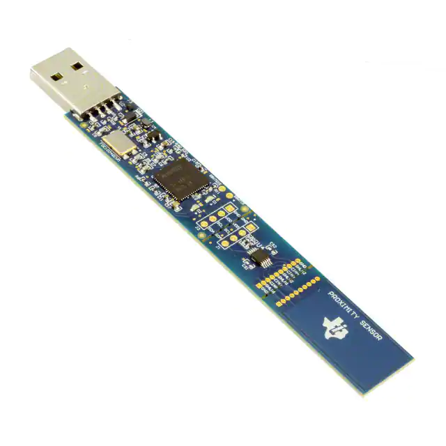
The FDC1004QEVM evaluation kit is a plug and play system to test and evaluate the FDC1004Q, AECQ100 qualified, 4-channel capacitive to digital converter. The EVM is a breakable PCB which consists of 3
sections. The first section is a USB to I2C converter based on MSP430F5528 micro-controller, the second
section contains the FDC1004Q and the third section is a touchless sensor (to demonstrate the sensitivity
of the FDC1004Q) . The third section can be removed and replace with customized sensors to evaluate
the capabilities of the FDC1004Q in various applications. The FDC1004QEVM can be used with the
FDC1004EVM GUI. The software is able to configure the FDC1004Q’s registers, display on four graphs
(one for each measurement) the capacitive values and export data in CSV format.
The EVM contains one FDC1004Q (See Table 1).
Table 1. Ordering
2
DEVICE
IC
Package
U1
FDC1004QDGS
VSSOP 10pin
Setup
This section provides a general description about FDC1004QEVM, its I/O connectors and how to properly
setup the evaluation module.
2.1
FDC1004QEVM
The FDC1004QEVM is divided in three sections:
1. USB to I2C section: this has the purpose to interface the communication of FDC1004Q to a USB port.
2. FDC1004Q section: this section embeds FDC1004Q capacitive to digital converter.
3. Sensor section: this section contains a capacitive sensor that can be used for human proximity.
The EVM has precut lines on the borders of each section that allow for a flexible and specific system
design. As an example of the flexibility of this design, the sensor can be replaced with a customer sensor,
or the MCU section can be separated to allow for a remote placement of the FDC1004Q.
4
FDC1004QEVM User's Guide
SNAU178 – April 2015
Submit Documentation Feedback
Copyright © 2015, Texas Instruments Incorporated
�Setup
www.ti.com
USB to I2C
FDC1004
SENSOR
Figure 1. FDC1004QEVM : Sections
2.2
Input/Output Connector Description
J1, J2: 4x1 Header: the I/O ports of sections between the USB to I2C and the FDC1004Q sections. This
provides the I2C communication channel and the power connections between these two sections should
the EVM be separated into sections. A simple 4 wire cable can be used to interface the sections.
Table 2. J1, J2 Pin Out
Pin
Pin
Description
J1.1
J2.1
GND
J1.2
J2.2
VDD
J1.3
J2.3
SCL
J1.4
J2.4
SDA
J3: USB interface to connect the EVM to a PC; it also provides power to the EVM.
J4: 10x1 Headers. This is not populated by default. It provides an easy method to change sensors or to
remotely place the sensor away from the FDC1004Q. This connector with its counterpart, J5, allows the
communication of the two modules through a 10-wire cable.
Table 3. J4 Pin Out
Pin
Description
J4.1
GND
J4.2
SHLD1
J4.3
CIN1
J4.4
CIN2
J4.5
SHLD1
J4.6
SHLD2
J4.7
CIN3
J4.8
CIN4
J4.9
SHLD2
J4.10
GND
J5: 10x1 Header, for the electrical connection between the FDC1004 and the sensor section.
SNAU178 – April 2015
Submit Documentation Feedback
FDC1004QEVM User's Guide
Copyright © 2015, Texas Instruments Incorporated
5
�Setup
www.ti.com
Table 4. J5 Pin Out
Pin
Description
J5.1
Not Connected
J5.2
SHLD1
J5.3
CIN1
J5.4
Not Connected
J5.5
SHLD1
J5.6
Not Connected
J5.7
Not Connected
J5.8
Not Connected
J5.9
Not Connected
J5.10
Not Connected
2.3
HW Setup
The power supply of FDC1004Q is provided by the LDO (U4), which is sourced from the USB 5.0V. The
I2C communication with FDC1004Q is fully managed by the MSP430F5528IRGC microcontroller (U3).
The FDC1004Q has a fixed I2C address.
2.4
SW Setup
Ensure that the FDC1004QEVM GUI and the drivers have been installed on the host computer. Plug the
EVM into an available USB port on the host.
2.5
Operation
Plug the EVM into the host computer. The host computer should automatically detect the device as an
EVM. Launch the GUI and configure the desired data acquisition mode for FDC1004Q. Then, it should
automatically start measuring on the configured sensors.
3
Board Layout
Figure 2 and Figure 3 show the board layout of the FDC1004QEVM.
Sensor layout has been designed to demonstrate human proximity sensing with a single sensor. A shield
layer below the sensor and a shield ring around the sensor is designed to significantly reduce parasitic
capacitance interference from directions not intended to sense the target. The intended sensing area for
this EVM is towards the top side of the sensor. For more information about shielding, refer to the
application note Capacitive Sensing: The Ins and Outs of Active Shielding (SNOA926).
Figure 2. Top Layer Routing
6
FDC1004QEVM User's Guide
SNAU178 – April 2015
Submit Documentation Feedback
Copyright © 2015, Texas Instruments Incorporated
�Board Layout
www.ti.com
Figure 3. Bottom Layer Routing
SNAU178 – April 2015
Submit Documentation Feedback
FDC1004QEVM User's Guide
Copyright © 2015, Texas Instruments Incorporated
7
�FID3
FDC1004QEVM User's Guide
Copyright © 2015, Texas Instruments Incorporated
COFF
100pF
GND GND
GND
5
4
CIN4
3
CIN2
CIN3
8
CIN1
C10
220pF
GND
GND
GND
SHLD2
SHLD1
7
6
1
9
10
GND
VDD
SCL
SDA
GND
C11
1300pF
VBUS
VUSB
VDD
11
15
40
53
54
55
17
51
50
52
9
10
57
58
12
13
34
35
36
37
38
AVCC1
DVCC1
DVCC2
VBUS
VUSB
V18
VCORE
PUR
PU.0/DP
PU.1/DM
P5.0/A8/VREF+/VEREF+
P5.1/A9/VREF-/VEREFP5.2/XT2IN
P5.3/XT2OUT
P5.4/XIN
P5.5/XOUT
P3.0/UCB0SIMO/UCB0SDA
P3.1/UCB0SOMI/UCB0SCL
P3.2/UCB0CLK/UCA0STE
P3.3/UCA0TXD/UCA0SIMO
P3.4/UCA0RXD/UCA0SOMI
GND
GND
CS2
51pF
SDA
CS1
GND
51pF
VDD
TSW-104-07-G-S
J2
R10
4.99k
SCL
1
2
3
4
MSP430F5528IRGC
SHLD1
SHLD2
R11
4.99k
GND
C19
1300pF
1.0k
R6
PUR
DP
DM
1.0k
R7
SCL
SDA
C6
1300pF
C17
0.47µF
FDC1004QDGS
CIN4
CIN3
CIN2
CIN1
VDD
U1
C8
18pF
GND
1
3
TSW-104-07-G-S
2
C1
0.1µF
G
G
24.000MHz
GND
J1
2
4
C20
1µF
1
2
3
4
C9
18pF
GND
Super Red
D2
Y1
Texas Instruments
PCB
LOGO
VDD
GND
VDD
SCL
SDA
GND
1
2
GND
Green
D1
Texas Instruments
PCB
LOGO
FID2
1
2
GND
GND
10
9
CIN4 8
CIN3 7
SHLD2
6
SHLD1
5
CIN2 4
CIN1 3
SHLD1
2
1
SHLD2
J4
QFN PAD
VSSU
AVSS1
AVSS2
DVSS1
DVSS2
RST/NMI/SBWTDIO
TEST/SBWTCK
PJ.0/TDO
PJ.1/TDI/TCLK
PJ.2/TMS
PJ.3/TCK
P6.0/CB0/A0
P6.1/CB1/A1
P6.2/CB2/A2
P6.3/CB3/A3
P6.4/CB4/A4
P6.5/CB5/A5
P6.6/CB6/A6
P6.7/CB7/A7
P4.0/PM_UCB1STE/PM_UCA1CLK
P4.1/PM_UCB1SIMO/PM_UCB1SDA
P4.2/PM_UCB1SOMI/PM_UCB1SCL
P4.3/PM_UCB1CLK/PM_UCA1STE
P4.4/PM_UCA1TXD/PM_UCA1SIMO
P4.5/PM_UCA1RXD/PM_UCA1SOMI
P4.6/PM_NONE
P4.7/PM_NONE
P2.0/TA1.1
P2.1/TA1.2
P2.2/TA2CLK/SMCLK
P2.3/TA2.0
P2.4/TA2.1
P2.5/TA2.2
P2.6/RTCCLK/DMAE0
P2.7/UCB0STE/UCA0CLK
65
49
14
56
16
39
64
59
60
61
62
63
1
2
3
4
5
6
7
8
J5
GND
C7
2200pF
R5
33k
SBWTDIO
VDD
SBWTCK
10
9
8
7
6
SHLD1
5
4
CIN1 3
SHLD1
2
1
GND
41
42 SDA
43 SCL
44
45
46
47
48
26
27
28
29
30
31
32
33
CIN1
SHLD1
J3
PROXIMITY
SENSOR
GND 48037-2200
5
6
GND
1
GND
U2
C3
3
1300pF
GND
C2
10µF
GND
VLS201610ET-100M
L1
D21
5.6V
MMSZ5232B-7-F
VBUS
GND
2
P1.0/TA0CLK/ACLK
P1.1/TA0.0
P1.2/TA0.1
P1.3/TA0.2
P1.4/TA0.3
P1.5/TA0.4
P1.6/TA1CLK/CBOUT
P1.7/TA1.0
3
FID1
4
U3
6
18
19
20
21
22
23
24
25
5
VCC
IO1
1
IO4
IO2
4
IO3
GND
2
8
3
GND
ON/OFF
IN
VBUS
C5
1300pF
GND
CBYP
OUT
R8
33
DM
C4
0.01µF
GND
R9
33
4
5
LP2985AIM5-3.3/NOPB
U4
GND
R20
33k
R40
33k
GND
C15
2.2µF
VDD
DP
PUR
4
2
PCB Number: SV601125
PCB Rev: A
Schematic
www.ti.com
Schematic
Figure 4. FDC1004QEVM Schematic
SNAU178 – April 2015
Submit Documentation Feedback
1
�Schematic
www.ti.com
Table 5. Bill of Materials
Qty
Designator
Description
Footprint
Manufacturer Part
Number
1
C1
CAP, CERM, 0.1uF, 6.3V, +/-10%, X5R, 0402
402
C1005X5R0J104K050BA
1
C2
CAP CER 10UF 10V 10% X5R 0603
603
C1608X5R1A106K080AC
4
C3, C5,
C11, C19
CAP CER 0.1UF 16V 5% X7R 0402
402
0402YC132KAT2A
1
C4
CAP, CERM, 0.01uF, 25V, +/-5%, C0G/NP0, 0603
603
C1608C0G1E103J080AA
1
C6
CAP CER 220PF 50V 1% NP0 0402
402
0402YC132KAT2A
1
C7
CAP, CERM, 2200pF, 50V, +/-10%, X7R, 0603
603
C0603X222K5RACTU
2
C8, C9
CAP CER 18PF 100V 5% NP0 0603
603
GRM1885C2A300JA01D
1
C10
CAP, CERM, 220pF, 50V, +/-1%, C0G/NP0, 0603
603
06035A221FAT2A
1
C15
CAP, CERM, 2.2uF, 10V, +/-10%, X5R, 0603
603
C0603C225K8PACTU
1
C17
CAP, CERM, 0.47uF, 10V, +/-10%, X7R, 0603
603
C0603C474K8RACTU
1
C20
CAP, CERM, 1uF, 6.3V, +/-20%, X5R, 0402
402
C1005X5R0J105M050BB
0
COFF
CAP, CERM, 100pF, 50V, +/-5%, C0G/NP0, 0402
402
GRM1535C1H101JDD5D
0
CS1, CS2
CAP, CERM, 51pF, 50V, +/-5%, C0G/NP0, 0402
402
GRM1555C1H510JA01D
1
D1
LED SMARTLED GREEN 570NM 0603
603
LG L29K-G2J1-24-Z
1
D2
LED 660NM SUPER RED DIFF 0603SMD
603
SML-LX0603SRW-TR
1
D21
Diode, Zener, 5.6V, 500mW, SOD-123
SOD-123
MMSZ5232B-7-F
0
J1, J2
Header, TH, 100mil, 4x1, Gold plated, 230 mil above
insulator
TSW-104-07-G-S
TSW-104-07-G-S
1
J3
Connector, USB Type A, 4POS R/A, SMD
CONN_USB_04803722
00
480372200
0
J4
Receptacle, 50mil 10x1, R/A, TH
CONN_851-43-010-20001000
851-43-010-20-001000
0
J5
Header, 50mil, 10x1, R/A, TH
CONN_850-80-010-20001101
850-80-010-20-001101
1
L1
INDUCTOR POWER 10UH .45A SMD
VLS201610E
VLS201610ET-100M
1
R5
RES, 33k ohm, 5%, 0.063W, 0402
402
CRCW040233K0JNED
2
R6, R7
RES 1K OHM 1/10W 5% 0402 SMD
402
CRCW040233R0JNED
2
R8, R9
RES, 33 ohm, 5%, 0.063W, 0402
402
CRCW040233R0JNED
2
R10, R11
RES, 4.99k ohm, 1%, 0.063W, 0402
402
CRCW04024K99FKED
1
R20
RES,1M ohm, 5%, 0.063W, 0402
402
RC0402JR-071ML
1
R40
RES 1.5K OHM 1/16W 5% 0402 SMD
402
CRCW04021K50JNED
1
U1
Q Grade 4-Channel Capacitance-to-Digital Converter
for Capacitive Sensing Solutions, DGS0010A
DGS0010A
FDC1004QDGS
1
U2
4-CHANNEL ESD-PROTECTION ARRAY FOR
HIGH-SPEED DATA INTERFACES, DRY006A
DRY0006A
TPD4E004DRY
1
U3
Mixed Signal MicroController, RGC0064B
RGC0064B
MSP430F5528IRGCT
1
U4
Micropower 150 mA Low-Noise Ultra Low-Dropout
Regulator, 5-pin SOT-23, Pb-Free
MF05A_N
LP2985AIM5-3.3/NOPB
1
Y1
CRYSTAL 24.000MHZ 18PF SMD
ABMM
ABMM-24.000MHZ-B2-T
SNAU178 – April 2015
Submit Documentation Feedback
FDC1004QEVM User's Guide
Copyright © 2015, Texas Instruments Incorporated
9
�Revision History
www.ti.com
Revision History
NOTE: Page numbers for previous revisions may differ from page numbers in the current version.
10
DATE
REVISION
NOTES
April 2015
*
Initial release.
Revision History
SNAU178 – April 2015
Submit Documentation Feedback
Copyright © 2015, Texas Instruments Incorporated
�STANDARD TERMS AND CONDITIONS FOR EVALUATION MODULES
1.
Delivery: TI delivers TI evaluation boards, kits, or modules, including any accompanying demonstration software, components, or
documentation (collectively, an “EVM” or “EVMs”) to the User (“User”) in accordance with the terms and conditions set forth herein.
Acceptance of the EVM is expressly subject to the following terms and conditions.
1.1 EVMs are intended solely for product or software developers for use in a research and development setting to facilitate feasibility
evaluation, experimentation, or scientific analysis of TI semiconductors products. EVMs have no direct function and are not
finished products. EVMs shall not be directly or indirectly assembled as a part or subassembly in any finished product. For
clarification, any software or software tools provided with the EVM (“Software”) shall not be subject to the terms and conditions
set forth herein but rather shall be subject to the applicable terms and conditions that accompany such Software
1.2 EVMs are not intended for consumer or household use. EVMs may not be sold, sublicensed, leased, rented, loaned, assigned,
or otherwise distributed for commercial purposes by Users, in whole or in part, or used in any finished product or production
system.
2
Limited Warranty and Related Remedies/Disclaimers:
2.1 These terms and conditions do not apply to Software. The warranty, if any, for Software is covered in the applicable Software
License Agreement.
2.2 TI warrants that the TI EVM will conform to TI's published specifications for ninety (90) days after the date TI delivers such EVM
to User. Notwithstanding the foregoing, TI shall not be liable for any defects that are caused by neglect, misuse or mistreatment
by an entity other than TI, including improper installation or testing, or for any EVMs that have been altered or modified in any
way by an entity other than TI. Moreover, TI shall not be liable for any defects that result from User's design, specifications or
instructions for such EVMs. Testing and other quality control techniques are used to the extent TI deems necessary or as
mandated by government requirements. TI does not test all parameters of each EVM.
2.3 If any EVM fails to conform to the warranty set forth above, TI's sole liability shall be at its option to repair or replace such EVM,
or credit User's account for such EVM. TI's liability under this warranty shall be limited to EVMs that are returned during the
warranty period to the address designated by TI and that are determined by TI not to conform to such warranty. If TI elects to
repair or replace such EVM, TI shall have a reasonable time to repair such EVM or provide replacements. Repaired EVMs shall
be warranted for the remainder of the original warranty period. Replaced EVMs shall be warranted for a new full ninety (90) day
warranty period.
3
Regulatory Notices:
3.1 United States
3.1.1
Notice applicable to EVMs not FCC-Approved:
This kit is designed to allow product developers to evaluate electronic components, circuitry, or software associated with the kit
to determine whether to incorporate such items in a finished product and software developers to write software applications for
use with the end product. This kit is not a finished product and when assembled may not be resold or otherwise marketed unless
all required FCC equipment authorizations are first obtained. Operation is subject to the condition that this product not cause
harmful interference to licensed radio stations and that this product accept harmful interference. Unless the assembled kit is
designed to operate under part 15, part 18 or part 95 of this chapter, the operator of the kit must operate under the authority of
an FCC license holder or must secure an experimental authorization under part 5 of this chapter.
3.1.2
For EVMs annotated as FCC – FEDERAL COMMUNICATIONS COMMISSION Part 15 Compliant:
CAUTION
This device complies with part 15 of the FCC Rules. Operation is subject to the following two conditions: (1) This device may not
cause harmful interference, and (2) this device must accept any interference received, including interference that may cause
undesired operation.
Changes or modifications not expressly approved by the party responsible for compliance could void the user's authority to
operate the equipment.
FCC Interference Statement for Class A EVM devices
NOTE: This equipment has been tested and found to comply with the limits for a Class A digital device, pursuant to part 15 of
the FCC Rules. These limits are designed to provide reasonable protection against harmful interference when the equipment is
operated in a commercial environment. This equipment generates, uses, and can radiate radio frequency energy and, if not
installed and used in accordance with the instruction manual, may cause harmful interference to radio communications.
Operation of this equipment in a residential area is likely to cause harmful interference in which case the user will be required to
correct the interference at his own expense.
SPACER
SPACER
SPACER
SPACER
SPACER
SPACER
SPACER
SPACER
�FCC Interference Statement for Class B EVM devices
NOTE: This equipment has been tested and found to comply with the limits for a Class B digital device, pursuant to part 15 of
the FCC Rules. These limits are designed to provide reasonable protection against harmful interference in a residential
installation. This equipment generates, uses and can radiate radio frequency energy and, if not installed and used in accordance
with the instructions, may cause harmful interference to radio communications. However, there is no guarantee that interference
will not occur in a particular installation. If this equipment does cause harmful interference to radio or television reception, which
can be determined by turning the equipment off and on, the user is encouraged to try to correct the interference by one or more
of the following measures:
•
•
•
•
Reorient or relocate the receiving antenna.
Increase the separation between the equipment and receiver.
Connect the equipment into an outlet on a circuit different from that to which the receiver is connected.
Consult the dealer or an experienced radio/TV technician for help.
3.2 Canada
3.2.1
For EVMs issued with an Industry Canada Certificate of Conformance to RSS-210
Concerning EVMs Including Radio Transmitters:
This device complies with Industry Canada license-exempt RSS standard(s). Operation is subject to the following two conditions:
(1) this device may not cause interference, and (2) this device must accept any interference, including interference that may
cause undesired operation of the device.
Concernant les EVMs avec appareils radio:
Le présent appareil est conforme aux CNR d'Industrie Canada applicables aux appareils radio exempts de licence. L'exploitation
est autorisée aux deux conditions suivantes: (1) l'appareil ne doit pas produire de brouillage, et (2) l'utilisateur de l'appareil doit
accepter tout brouillage radioélectrique subi, même si le brouillage est susceptible d'en compromettre le fonctionnement.
Concerning EVMs Including Detachable Antennas:
Under Industry Canada regulations, this radio transmitter may only operate using an antenna of a type and maximum (or lesser)
gain approved for the transmitter by Industry Canada. To reduce potential radio interference to other users, the antenna type
and its gain should be so chosen that the equivalent isotropically radiated power (e.i.r.p.) is not more than that necessary for
successful communication. This radio transmitter has been approved by Industry Canada to operate with the antenna types
listed in the user guide with the maximum permissible gain and required antenna impedance for each antenna type indicated.
Antenna types not included in this list, having a gain greater than the maximum gain indicated for that type, are strictly prohibited
for use with this device.
Concernant les EVMs avec antennes détachables
Conformément à la réglementation d'Industrie Canada, le présent émetteur radio peut fonctionner avec une antenne d'un type et
d'un gain maximal (ou inférieur) approuvé pour l'émetteur par Industrie Canada. Dans le but de réduire les risques de brouillage
radioélectrique à l'intention des autres utilisateurs, il faut choisir le type d'antenne et son gain de sorte que la puissance isotrope
rayonnée équivalente (p.i.r.e.) ne dépasse pas l'intensité nécessaire à l'établissement d'une communication satisfaisante. Le
présent émetteur radio a été approuvé par Industrie Canada pour fonctionner avec les types d'antenne énumérés dans le
manuel d’usage et ayant un gain admissible maximal et l'impédance requise pour chaque type d'antenne. Les types d'antenne
non inclus dans cette liste, ou dont le gain est supérieur au gain maximal indiqué, sont strictement interdits pour l'exploitation de
l'émetteur
3.3 Japan
3.3.1
Notice for EVMs delivered in Japan: Please see http://www.tij.co.jp/lsds/ti_ja/general/eStore/notice_01.page 日本国内に
輸入される評価用キット、ボードについては、次のところをご覧ください。
http://www.tij.co.jp/lsds/ti_ja/general/eStore/notice_01.page
3.3.2
Notice for Users of EVMs Considered “Radio Frequency Products” in Japan: EVMs entering Japan may not be certified
by TI as conforming to Technical Regulations of Radio Law of Japan.
If User uses EVMs in Japan, not certified to Technical Regulations of Radio Law of Japan, User is required by Radio Law of
Japan to follow the instructions below with respect to EVMs:
1.
2.
3.
Use EVMs in a shielded room or any other test facility as defined in the notification #173 issued by Ministry of Internal
Affairs and Communications on March 28, 2006, based on Sub-section 1.1 of Article 6 of the Ministry’s Rule for
Enforcement of Radio Law of Japan,
Use EVMs only after User obtains the license of Test Radio Station as provided in Radio Law of Japan with respect to
EVMs, or
Use of EVMs only after User obtains the Technical Regulations Conformity Certification as provided in Radio Law of Japan
with respect to EVMs. Also, do not transfer EVMs, unless User gives the same notice above to the transferee. Please note
that if User does not follow the instructions above, User will be subject to penalties of Radio Law of Japan.
SPACER
SPACER
SPACER
SPACER
SPACER
�【無線電波を送信する製品の開発キットをお使いになる際の注意事項】 開発キットの中には技術基準適合証明を受けて
いないものがあります。 技術適合証明を受けていないもののご使用に際しては、電波法遵守のため、以下のいずれかの
措置を取っていただく必要がありますのでご注意ください。
1.
2.
3.
電波法施行規則第6条第1項第1号に基づく平成18年3月28日総務省告示第173号で定められた電波暗室等の試験設備でご使用
いただく。
実験局の免許を取得後ご使用いただく。
技術基準適合証明を取得後ご使用いただく。
なお、本製品は、上記の「ご使用にあたっての注意」を譲渡先、移転先に通知しない限り、譲渡、移転できないものとします。
上記を遵守頂けない場合は、電波法の罰則が適用される可能性があることをご留意ください。 日本テキサス・イ
ンスツルメンツ株式会社
東京都新宿区西新宿6丁目24番1号
西新宿三井ビル
3.3.3
Notice for EVMs for Power Line Communication: Please see http://www.tij.co.jp/lsds/ti_ja/general/eStore/notice_02.page
電力線搬送波通信についての開発キットをお使いになる際の注意事項については、次のところをご覧くださ
い。http://www.tij.co.jp/lsds/ti_ja/general/eStore/notice_02.page
SPACER
4
EVM Use Restrictions and Warnings:
4.1 EVMS ARE NOT FOR USE IN FUNCTIONAL SAFETY AND/OR SAFETY CRITICAL EVALUATIONS, INCLUDING BUT NOT
LIMITED TO EVALUATIONS OF LIFE SUPPORT APPLICATIONS.
4.2 User must read and apply the user guide and other available documentation provided by TI regarding the EVM prior to handling
or using the EVM, including without limitation any warning or restriction notices. The notices contain important safety information
related to, for example, temperatures and voltages.
4.3 Safety-Related Warnings and Restrictions:
4.3.1
User shall operate the EVM within TI’s recommended specifications and environmental considerations stated in the user
guide, other available documentation provided by TI, and any other applicable requirements and employ reasonable and
customary safeguards. Exceeding the specified performance ratings and specifications (including but not limited to input
and output voltage, current, power, and environmental ranges) for the EVM may cause personal injury or death, or
property damage. If there are questions concerning performance ratings and specifications, User should contact a TI
field representative prior to connecting interface electronics including input power and intended loads. Any loads applied
outside of the specified output range may also result in unintended and/or inaccurate operation and/or possible
permanent damage to the EVM and/or interface electronics. Please consult the EVM user guide prior to connecting any
load to the EVM output. If there is uncertainty as to the load specification, please contact a TI field representative.
During normal operation, even with the inputs and outputs kept within the specified allowable ranges, some circuit
components may have elevated case temperatures. These components include but are not limited to linear regulators,
switching transistors, pass transistors, current sense resistors, and heat sinks, which can be identified using the
information in the associated documentation. When working with the EVM, please be aware that the EVM may become
very warm.
4.3.2
EVMs are intended solely for use by technically qualified, professional electronics experts who are familiar with the
dangers and application risks associated with handling electrical mechanical components, systems, and subsystems.
User assumes all responsibility and liability for proper and safe handling and use of the EVM by User or its employees,
affiliates, contractors or designees. User assumes all responsibility and liability to ensure that any interfaces (electronic
and/or mechanical) between the EVM and any human body are designed with suitable isolation and means to safely
limit accessible leakage currents to minimize the risk of electrical shock hazard. User assumes all responsibility and
liability for any improper or unsafe handling or use of the EVM by User or its employees, affiliates, contractors or
designees.
4.4 User assumes all responsibility and liability to determine whether the EVM is subject to any applicable international, federal,
state, or local laws and regulations related to User’s handling and use of the EVM and, if applicable, User assumes all
responsibility and liability for compliance in all respects with such laws and regulations. User assumes all responsibility and
liability for proper disposal and recycling of the EVM consistent with all applicable international, federal, state, and local
requirements.
5.
Accuracy of Information: To the extent TI provides information on the availability and function of EVMs, TI attempts to be as accurate
as possible. However, TI does not warrant the accuracy of EVM descriptions, EVM availability or other information on its websites as
accurate, complete, reliable, current, or error-free.
SPACER
SPACER
SPACER
SPACER
SPACER
SPACER
�SPACER
6.
Disclaimers:
6.1 EXCEPT AS SET FORTH ABOVE, EVMS AND ANY WRITTEN DESIGN MATERIALS PROVIDED WITH THE EVM (AND THE
DESIGN OF THE EVM ITSELF) ARE PROVIDED "AS IS" AND "WITH ALL FAULTS." TI DISCLAIMS ALL OTHER
WARRANTIES, EXPRESS OR IMPLIED, REGARDING SUCH ITEMS, INCLUDING BUT NOT LIMITED TO ANY IMPLIED
WARRANTIES OF MERCHANTABILITY OR FITNESS FOR A PARTICULAR PURPOSE OR NON-INFRINGEMENT OF ANY
THIRD PARTY PATENTS, COPYRIGHTS, TRADE SECRETS OR OTHER INTELLECTUAL PROPERTY RIGHTS.
6.2 EXCEPT FOR THE LIMITED RIGHT TO USE THE EVM SET FORTH HEREIN, NOTHING IN THESE TERMS AND
CONDITIONS SHALL BE CONSTRUED AS GRANTING OR CONFERRING ANY RIGHTS BY LICENSE, PATENT, OR ANY
OTHER INDUSTRIAL OR INTELLECTUAL PROPERTY RIGHT OF TI, ITS SUPPLIERS/LICENSORS OR ANY OTHER THIRD
PARTY, TO USE THE EVM IN ANY FINISHED END-USER OR READY-TO-USE FINAL PRODUCT, OR FOR ANY
INVENTION, DISCOVERY OR IMPROVEMENT MADE, CONCEIVED OR ACQUIRED PRIOR TO OR AFTER DELIVERY OF
THE EVM.
7.
USER'S INDEMNITY OBLIGATIONS AND REPRESENTATIONS. USER WILL DEFEND, INDEMNIFY AND HOLD TI, ITS
LICENSORS AND THEIR REPRESENTATIVES HARMLESS FROM AND AGAINST ANY AND ALL CLAIMS, DAMAGES, LOSSES,
EXPENSES, COSTS AND LIABILITIES (COLLECTIVELY, "CLAIMS") ARISING OUT OF OR IN CONNECTION WITH ANY
HANDLING OR USE OF THE EVM THAT IS NOT IN ACCORDANCE WITH THESE TERMS AND CONDITIONS. THIS OBLIGATION
SHALL APPLY WHETHER CLAIMS ARISE UNDER STATUTE, REGULATION, OR THE LAW OF TORT, CONTRACT OR ANY
OTHER LEGAL THEORY, AND EVEN IF THE EVM FAILS TO PERFORM AS DESCRIBED OR EXPECTED.
8.
Limitations on Damages and Liability:
8.1 General Limitations. IN NO EVENT SHALL TI BE LIABLE FOR ANY SPECIAL, COLLATERAL, INDIRECT, PUNITIVE,
INCIDENTAL, CONSEQUENTIAL, OR EXEMPLARY DAMAGES IN CONNECTION WITH OR ARISING OUT OF THESE
TERMS ANDCONDITIONS OR THE USE OF THE EVMS PROVIDED HEREUNDER, REGARDLESS OF WHETHER TI HAS
BEEN ADVISED OF THE POSSIBILITY OF SUCH DAMAGES. EXCLUDED DAMAGES INCLUDE, BUT ARE NOT LIMITED
TO, COST OF REMOVAL OR REINSTALLATION, ANCILLARY COSTS TO THE PROCUREMENT OF SUBSTITUTE GOODS
OR SERVICES, RETESTING, OUTSIDE COMPUTER TIME, LABOR COSTS, LOSS OF GOODWILL, LOSS OF PROFITS,
LOSS OF SAVINGS, LOSS OF USE, LOSS OF DATA, OR BUSINESS INTERRUPTION. NO CLAIM, SUIT OR ACTION SHALL
BE BROUGHT AGAINST TI MORE THAN ONE YEAR AFTER THE RELATED CAUSE OF ACTION HAS OCCURRED.
8.2 Specific Limitations. IN NO EVENT SHALL TI'S AGGREGATE LIABILITY FROM ANY WARRANTY OR OTHER OBLIGATION
ARISING OUT OF OR IN CONNECTION WITH THESE TERMS AND CONDITIONS, OR ANY USE OF ANY TI EVM
PROVIDED HEREUNDER, EXCEED THE TOTAL AMOUNT PAID TO TI FOR THE PARTICULAR UNITS SOLD UNDER
THESE TERMS AND CONDITIONS WITH RESPECT TO WHICH LOSSES OR DAMAGES ARE CLAIMED. THE EXISTENCE
OF MORE THAN ONE CLAIM AGAINST THE PARTICULAR UNITS SOLD TO USER UNDER THESE TERMS AND
CONDITIONS SHALL NOT ENLARGE OR EXTEND THIS LIMIT.
9.
Return Policy. Except as otherwise provided, TI does not offer any refunds, returns, or exchanges. Furthermore, no return of EVM(s)
will be accepted if the package has been opened and no return of the EVM(s) will be accepted if they are damaged or otherwise not in
a resalable condition. If User feels it has been incorrectly charged for the EVM(s) it ordered or that delivery violates the applicable
order, User should contact TI. All refunds will be made in full within thirty (30) working days from the return of the components(s),
excluding any postage or packaging costs.
10. Governing Law: These terms and conditions shall be governed by and interpreted in accordance with the laws of the State of Texas,
without reference to conflict-of-laws principles. User agrees that non-exclusive jurisdiction for any dispute arising out of or relating to
these terms and conditions lies within courts located in the State of Texas and consents to venue in Dallas County, Texas.
Notwithstanding the foregoing, any judgment may be enforced in any United States or foreign court, and TI may seek injunctive relief
in any United States or foreign court.
Mailing Address: Texas Instruments, Post Office Box 655303, Dallas, Texas 75265
Copyright © 2015, Texas Instruments Incorporated
spacer
�IMPORTANT NOTICE
Texas Instruments Incorporated and its subsidiaries (TI) reserve the right to make corrections, enhancements, improvements and other
changes to its semiconductor products and services per JESD46, latest issue, and to discontinue any product or service per JESD48, latest
issue. Buyers should obtain the latest relevant information before placing orders and should verify that such information is current and
complete. All semiconductor products (also referred to herein as “components”) are sold subject to TI’s terms and conditions of sale
supplied at the time of order acknowledgment.
TI warrants performance of its components to the specifications applicable at the time of sale, in accordance with the warranty in TI’s terms
and conditions of sale of semiconductor products. Testing and other quality control techniques are used to the extent TI deems necessary
to support this warranty. Except where mandated by applicable law, testing of all parameters of each component is not necessarily
performed.
TI assumes no liability for applications assistance or the design of Buyers’ products. Buyers are responsible for their products and
applications using TI components. To minimize the risks associated with Buyers’ products and applications, Buyers should provide
adequate design and operating safeguards.
TI does not warrant or represent that any license, either express or implied, is granted under any patent right, copyright, mask work right, or
other intellectual property right relating to any combination, machine, or process in which TI components or services are used. Information
published by TI regarding third-party products or services does not constitute a license to use such products or services or a warranty or
endorsement thereof. Use of such information may require a license from a third party under the patents or other intellectual property of the
third party, or a license from TI under the patents or other intellectual property of TI.
Reproduction of significant portions of TI information in TI data books or data sheets is permissible only if reproduction is without alteration
and is accompanied by all associated warranties, conditions, limitations, and notices. TI is not responsible or liable for such altered
documentation. Information of third parties may be subject to additional restrictions.
Resale of TI components or services with statements different from or beyond the parameters stated by TI for that component or service
voids all express and any implied warranties for the associated TI component or service and is an unfair and deceptive business practice.
TI is not responsible or liable for any such statements.
Buyer acknowledges and agrees that it is solely responsible for compliance with all legal, regulatory and safety-related requirements
concerning its products, and any use of TI components in its applications, notwithstanding any applications-related information or support
that may be provided by TI. Buyer represents and agrees that it has all the necessary expertise to create and implement safeguards which
anticipate dangerous consequences of failures, monitor failures and their consequences, lessen the likelihood of failures that might cause
harm and take appropriate remedial actions. Buyer will fully indemnify TI and its representatives against any damages arising out of the use
of any TI components in safety-critical applications.
In some cases, TI components may be promoted specifically to facilitate safety-related applications. With such components, TI’s goal is to
help enable customers to design and create their own end-product solutions that meet applicable functional safety standards and
requirements. Nonetheless, such components are subject to these terms.
No TI components are authorized for use in FDA Class III (or similar life-critical medical equipment) unless authorized officers of the parties
have executed a special agreement specifically governing such use.
Only those TI components which TI has specifically designated as military grade or “enhanced plastic” are designed and intended for use in
military/aerospace applications or environments. Buyer acknowledges and agrees that any military or aerospace use of TI components
which have not been so designated is solely at the Buyer's risk, and that Buyer is solely responsible for compliance with all legal and
regulatory requirements in connection with such use.
TI has specifically designated certain components as meeting ISO/TS16949 requirements, mainly for automotive use. In any case of use of
non-designated products, TI will not be responsible for any failure to meet ISO/TS16949.
Products
Applications
Audio
www.ti.com/audio
Automotive and Transportation
www.ti.com/automotive
Amplifiers
amplifier.ti.com
Communications and Telecom
www.ti.com/communications
Data Converters
dataconverter.ti.com
Computers and Peripherals
www.ti.com/computers
DLP® Products
www.dlp.com
Consumer Electronics
www.ti.com/consumer-apps
DSP
dsp.ti.com
Energy and Lighting
www.ti.com/energy
Clocks and Timers
www.ti.com/clocks
Industrial
www.ti.com/industrial
Interface
interface.ti.com
Medical
www.ti.com/medical
Logic
logic.ti.com
Security
www.ti.com/security
Power Mgmt
power.ti.com
Space, Avionics and Defense
www.ti.com/space-avionics-defense
Microcontrollers
microcontroller.ti.com
Video and Imaging
www.ti.com/video
RFID
www.ti-rfid.com
OMAP Applications Processors
www.ti.com/omap
TI E2E Community
e2e.ti.com
Wireless Connectivity
www.ti.com/wirelessconnectivity
Mailing Address: Texas Instruments, Post Office Box 655303, Dallas, Texas 75265
Copyright © 2015, Texas Instruments Incorporated
�


 工商网监
湘ICP备2023018690号
工商网监
湘ICP备2023018690号
