FPC402
FPC402
SNLS582C – JUNE 2017 – REVISED SEPTEMBER
2020
SNLS582C – JUNE 2017 – REVISED SEPTEMBER 2020
www.ti.com
FPC402 Quad Port Controller
1 Features
3 Description
•
The FPC402 quad port controller serves as a lowspeed signal aggregator for common port types such
as SFP, QSFP, Mini-SAS HD, and others. The
FPC402 aggregates all low-speed control and I2C
signals across four ports and presents a single easyto-use management interface to the host (I2C or SPI).
Multiple FPC402s can be used in high-port-count
applications with one common control interface to the
host. The FPC402 is designed to allow placement on
the bottom side of the PCB, underneath the press fit
connector, to simplify routing. This localized control of
the low-speed signals in the ports cuts system BOM
costs by enabling the use of smaller IO count control
devices (FPGAs, CPLDs, and MCUs) and by reducing
routing layer congestion.
•
•
•
•
•
•
•
•
•
•
Control Signal Management and I2C Aggregation
Across Four Ports
Combine Multiple FPC402s to Control 56 Total
Ports Through a Single Host Interface
Eliminate Need for Discrete I2C Muxes, LED
Drivers, and High-Pin-Count FPGA/CPLD Control
Devices
Reduce PCB Routing Complexity by Handling All
Low-Speed Control Signals Close to the Port
Selectable I2C (up to 1 MHz) or SPI (up to 10
MHz) Host Control Interface
Automatic Prefetching of Critical, User-Specified
Data From the Modules
Broadcast Mode Write to All Ports Simultaneously
Across All FPC402 Controllers
Advanced LED Features for Port Status Indication,
Including Programmable Blinking and Dimming
Customizable Interrupt Events
Separate Host-Side I/O Voltage: 1.8 V to 3.3 V
Small WQFN Package Enabling Placement on
Bottom Side of PCB Underneath Ports
2 Applications
•
•
•
•
•
ToR/Aggregation/Core Switch and Router
Wireless Infrastructure Base Band Unit and
Remote Radio Unit
Video Switch and Router
Storage Cards and Storage Racks
SFP, QSFP, QSFP-DD, OSFP, Mini-SAS HD Port
Management
Device Information (1)
PART NUMBER
FPC402
(1)
PACKAGE
BODY SIZE (NOM)
WQFN (56)
5.00 mm × 11.00 mm
For all available packages, see the orderable addendum at
the end of the data sheet.
Device Comparison
PART
NUMBER
ACCESSIBLE DOWNSTREAM
ADDRESSES
PIN
COMPATIBLE
FPC402
All valid I2C addreses
Yes
FPC401
MSA Addresses: 0xA0, 0xA2
Yes
HOST
CONTROLLER
INT
SCL
SDA
FPC402 QUAD PORT CONTROLLER
PORT 0
PORT 1
PORT 2
FPC402 QUAD PORT CONTROLLER
PORT 3
PORT 0
PORT 1
PORT 2
I2C,
STATUS,
CONTROL
PORT 3
I2C,
STATUS,
CONTROL
SFP,
QSFP,
QSFP-DD,
OSFP
SFP,
QSFP,
QSFP-DD,
OSFP
SFP,
QSFP,
QSFP-DD,
OSFP
SFP,
QSFP,
QSFP-DD,
OSFP
SFP,
QSFP,
QSFP-DD,
OSFP
SFP,
QSFP,
QSFP-DD,
OSFP
PORT 0
PORT 1
PORT2
PORT 3
PORT 4
PORT 5
SFP,
QSFP,
QSFP-DD,
OSFP
SFP,
QSFP,
QSFP-DD,
OSFP
PORT 6
PORT 7
Copyright © 2017, Texas Instruments Incorporated
Simplified Block Diagram
An IMPORTANT NOTICE at the end of this data sheet addresses availability, warranty, changes, use in safety-critical applications,
Submit Document Feedback
Copyright
© 2020 Texas
Instruments
Incorporated
intellectual
property
matters
and other important disclaimers. PRODUCTION DATA.
Product Folder Links: FPC402
1
�FPC402
www.ti.com
SNLS582C – JUNE 2017 – REVISED SEPTEMBER 2020
Table of Contents
1 Features............................................................................1
2 Applications..................................................................... 1
3 Description.......................................................................1
4 Revision History.............................................................. 2
5 Description (continued).................................................. 2
6 Pin Configuration and Functions...................................3
Pin Functions.................................................................... 3
7 Specifications.................................................................. 6
7.1 Absolute Maximum Ratings........................................ 6
7.2 ESD Ratings............................................................... 6
7.3 Recommended Operating Conditions.........................6
7.4 Thermal Information....................................................7
7.5 Electrical Characteristics.............................................7
7.6 Timing Requirements.................................................. 9
7.7 Switching Characteristics..........................................10
7.8 Typical Characteristics.............................................. 11
8 Detailed Description......................................................12
8.1 Overview................................................................... 12
8.2 Functional Block Diagram......................................... 12
8.3 Feature Description...................................................13
8.4 Device Functional Modes..........................................21
8.5 Programming............................................................ 27
9 Application and Implementation.................................. 28
9.1 Application Information............................................. 28
9.2 Typical Application.................................................... 28
10 Power Supply Recommendations..............................33
10.1 Power Supply Sequencing......................................33
11 Layout........................................................................... 34
11.1 Layout Guidelines................................................... 34
11.2 Layout Example...................................................... 35
11.3 Recommended Package Footprint..........................36
12 Device and Documentation Support..........................37
12.1 Documentation Support.......................................... 37
12.2 Receiving Notification of Documentation Updates..37
12.3 Support Resources................................................. 37
12.4 Trademarks............................................................. 37
12.5 Electrostatic Discharge Caution..............................37
12.6 Glossary..................................................................37
13 Mechanical, Packaging, and Orderable
Information.................................................................... 37
4 Revision History
Changes from Revision B (August 2018) to Revision C (September 2020)
Page
• Released the full production data data sheet to ti.com.......................................................................................1
• Updated the numbering format for tables, figures, and cross-references throughout the document..................1
• Added the recommended foot print for RHU package......................................................................................36
Changes from Revision A (October 2017) to Revision B (August 2018)
Page
• Changed MOD_SDA[0] pin number from: 16 to: 35 .......................................................................................... 3
• Changed MOD_SDA[1] pin number from: 5 to: 48............................................................................................. 3
• Changed MOD_SDA[2] pin number from: 48 to: 5............................................................................................. 3
• Changed MOD_SDA[3] pin number from: 35 to: 16........................................................................................... 3
Changes from Revision * (June 2017) to Revision A (October 2017)
Page
• Changed Advance Information to Production Data ........................................................................................... 1
• Updated TPOR (max) .......................................................................................................................................... 9
5 Description (continued)
The FPC402 is compatible with standard SFF-8431, SFF-8436, and SFF-8449 low-speed management
interfaces, including a dedicated 100- or 400-kHz I2C interface to each port. Additional general-purpose pins are
available to perform functions such as driving port status LEDs or controlling power switches. The LED drivers
have convenience features such as programmable blinking and dimming. The interface to the host controller can
operate on a separate supply voltage between 1.8 V and 3.3 V to support low-voltage I/Os.
The FPC402 can prefetch data from user-specified registers in each module, making the data readily accessible
to the host through a fast I2C (up to 1 MHz) or SPI (up to 10 MHz) interface. In addition, the FPC402 can trigger
an interrupt to the host whenever critical, user-configurable events occur associated with any of the ports the
device controls. This eliminates the need to continuously poll the modules.
2
Submit Document Feedback
Copyright © 2020 Texas Instruments Incorporated
Product Folder Links: FPC402
�FPC402
www.ti.com
SNLS582C – JUNE 2017 – REVISED SEPTEMBER 2020
OUT_A[2]
IN_A[2]
VDD1
GPIO[1]
OUT_D[1]
OUT_C[1]
IN_A[1]
MOD_SCL[1]
56
55
54
53
52
51
50
49
6 Pin Configuration and Functions
IN_B[2]
1
48
MOD_SDA[1]
OUT_B[2]
2
47
IN_B[1]
IN_C[2]
3
46
IN_C[1]
MOD_SCL[2]
4
45
OUT_B[1]
MOD_SDA[2]
5
44
OUT_A[1]
OUT_C[2]
6
43
VDD1
OUT_D[2]
7
42
GPIO[0]
GPIO[2]
8
41
IN_A[0]
VDD1
9
40
OUT_A[0]
IN_A[3]
10
39
IN_B[0]
OUT_A[3]
11
38
OUT_B[0]
IN_B[3]
12
37
IN_C[0]
OUT_B[3]
13
36
MOD_SCL[0]
IN_C[3]
14
35
MOD_SDA[0]
MOD_SCL[3]
15
34
OUT_C[0]
MOD_SDA[3]
16
33
OUT_D[0]
OUT_C[3]
17
32
CAPL
OUT_D[3]
18
31
PROTOCOL_SEL
GPIO[3]
19
30
SPI_LED_SYNC
VDD2
20
29
TEST_N
23
24
25
26
27
CTRL1
CTRL2
HOST_INT_N
VDD2
GND
28
22
EN
CTRL3
21
CTRL4
Die Attach Pad (DAP) =
GND
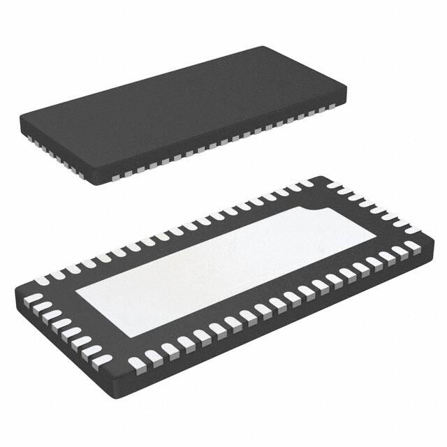
Figure 6-1. RHU Package 56-Pin WQFN Top View
Pin Functions
PIN
NAME
NO.
CAPL
32
I/O
O
DESCRIPTION
Connect a single 2.2-µF capacitor to GND.
Submit Document Feedback
Copyright © 2020 Texas Instruments Incorporated
Product Folder Links: FPC402
3
�FPC402
www.ti.com
SNLS582C – JUNE 2017 – REVISED SEPTEMBER 2020
PIN
I/O
NAME
NO.
CTRL1
23
I/O
CTRL2
24
I/O
CTRL3
28
I, Weak
internal
pullup
DESCRIPTION
Host-side control interface. These pins are used to implement I2C or SPI depending on the
PROTOCOL_SEL pin configuration.
I2C mode (PROTOCOL_SEL = Float or High):
CTRL1: SCL – I2C Clock input / open-drain output
CTRL2: SDA – I2C Data input / open-drain output
CTRL3: SET_ADDR_N – input, address assignment enable. Also used to receive external LED
clock.
CTRL4: ADDR_DONE_N – output, address assignment complete. Also used to transmit LED
clock.
CTRL4
21
O
SPI mode (PROTOCOL_SEL = GND):
CTRL1: SCK – Serial clock input
CTRL2: SS_N – Active-low slave select input
CTRL3: MOSI – Master output or slave input
CTRL4: MISO – Master input or slave output
EN
I, Weak
internal
pullup
22
Device enable. When EN = 0, the FPC402 is in a power-down state and does not respond to
the host-side control bus, nor does it perform port-side I2C accesses. When EN=VDD2 or
Float, the FPC402 is fully enabled and will respond to the host-side control bus provided VDD1
and VDD2 power has been stable for at least TPOR. VIH for this pin is referenced to VDD2.
The minimum required assert and deassert time is 12.5 µs.
GPIO[0]
42
GPIO[1]
53
GPIO[2]
8
GPIO[3]
19
GND
4
27, DAP
HOST_INT_N
25
IN_A[0]
41
IN_A[1]
50
IN_A[2]
55
IN_A[3]
10
IN_B[0]
39
IN_B[1]
47
IN_B[2]
1
IN_B[3]
12
IN_C[0]
37
IN_C[1]
46
IN_C[2]
3
IN_C[3]
14
MOD_SCL[0]
36
MOD_SCL[1]
49
MOD_SCL[2]
4
MOD_SCL[3]
15
I/O
General-purpose I/O. Output high voltage (VOH) and input high voltage (VIH) are based on
VDD1. Configured as input (high-Z) by default.
Power
Ground reference. The GND pins must be connected through a low-resistance path to the
board GND plane.
Open-drain 3.3-V tolerant active-low interrupt output. It asserts low to interrupt the host. The
O, Open- events which trigger an interrupt are programmable through registers. This pin can be
Drain
connected in a wired-OR fashion with other FPC402s’ interrupt pins. A single pullup resistor to
VDD1 or VDD2 in the 2-kΩ to 5-kΩ range is adequate for the entire net.
Low-speed port status input A.
I, Weak
internal
pullup
Example usage:
SFP: Mod_ABS[3:0]
QSFP: ModPrsL[3:0]
Low-speed port status input B.
I, Weak
internal
pullup
Example usage:
SFP: Tx_Fault[3:0]
QSFP: IntL[3:0]
Low-speed port status input C.
I, Weak
internal
pullup
Example usage:
SFP: Rx_LOS[3:0]
QSFP: N/A
I/O,
OpenDrain
I2C clock open-drain output to the module. External 2-kΩ to 5-kΩ pullup resistor is required.
This pin is 3.3-V LVCMOS tolerant.
Submit Document Feedback
Copyright © 2020 Texas Instruments Incorporated
Product Folder Links: FPC402
�FPC402
www.ti.com
SNLS582C – JUNE 2017 – REVISED SEPTEMBER 2020
PIN
NAME
NO.
MOD_SDA[0]
35
MOD_SDA[1]
48
MOD_SDA[2]
5
MOD_SDA[3]
16
OUT_A[0]
40
OUT_A[1]
44
OUT_A[2]
56
OUT_A[3]
11
I/O
I/O,
OpenDrain
DESCRIPTION
I2C data input or open-drain output to the module. External 2-kΩ to 5-kΩ pullup resistor is
required. This pin is 3.3-V LVCMOS tolerant.
Low-speed port control output A. OUT_A is disabled by default (high-Z) and when enabled
drives high logic unless reprogrammed. A 10-kΩ pullup or pulldown resistor is recommended to
set a default logic value before this output is enabled. See Section 8.3.3 for more details.
O
Example usage:
SFP: Tx_Disable[3:0]
QSFP: ResetL[3:0]
OUT_B[0]
38
OUT_B[1]
45
OUT_B[2]
2
OUT_B[3]
13
Low-speed port control output B. Output is disabled by default (high-Z) and when enabled
drives low logic unless reprogrammed. A 10-kΩ pullup or pulldown resistor is recommended to
set a default logic value before this output is enabled. See Section 8.3.3 for more details.
O
Example usage:
SFP: RS[3:0]
QSFP: LPMode[3:0]
OUT_C[0]
34
OUT_C[1]
51
OUT_C[2]
6
Low-speed port control output C. Can be used to drive port status LED. Special LED driving
features are available on this output. This output is enabled and high logic by default at power
up. See Section 8.3.2 for more details.
Example usage:
O
OUT_C[3]
SFP: LED_GRN[3:0]
QSFP: LED_GRN[3:0]
17
This pin requires a series resistor with a value of at least 33 Ω. The LED current-limiting
resistor can serve for this purpose.
OUT_D[0]
33
OUT_D[1]
52
OUT_D[2]
7
Low-speed port control output D. Can be used to drive port status LED. Special LED driving
features are available on this output. This output is enabled and high logic by default at power
up. See Section 8.3.2 for more details.
Example usage:
O
OUT_D[3]
SFP: LED_YLW[3:0]
QSFP: N/A
18
This pin requires a series resistor with a value of at least 33 Ω. The LED current-limiting
resistor can serve for this purpose.
PROTOCOL_SEL
31
I, Weak
internal
pullup
Used to select between I2C and SPI host-side control interface.
Float or High: Inter-IC Control (I2C)
GND: Serial Peripheral Interface (SPI)
LED clock synchronization pin for SPI mode only.
SPI_LED_SYNC
30
I/O
When using SPI as the host-side control interface (PROTOCOL_SEL=GND), connect all
FPC402 SPI_LED_CLK pins together. This ensures LED synchronization across all FPC402
devices.
When using I2C as the host-side control interface, this pin can be floating. LED
synchronization is ensured by other means in I2C mode.
TEST_N
VDD1
29
I, Weak
internal
pullup
TI test mode.
Float or High: Normal operation
GND: TI Test Mode
9, 43, 54
Power
Main power supply, VDD1 = 3.3 V ± 5%. TI recommends connecting at least one 1-µF and one
0.1-µF decoupling capacitors per VDD1 pin as close to the pin as possible.
Submit Document Feedback
Copyright © 2020 Texas Instruments Incorporated
Product Folder Links: FPC402
5
�FPC402
www.ti.com
SNLS582C – JUNE 2017 – REVISED SEPTEMBER 2020
PIN
NAME
NO.
VDD2
20, 26
I/O
DESCRIPTION
Power
Power supply for host-side interface I/Os (CTRL[4:1]). VDD2 can be 1.8 V to 3.3 V ± 5%. If the
host-side interface operates at 3.3 V, then VDD1 and VDD2 can be connected to the same 3.3V ± 5% supply. TI recommends connecting at least one 1-µF and one 0.1-µF decoupling
capacitors per VDD2 pin as close to the pin as possible.
7 Specifications
7.1 Absolute Maximum Ratings
over operating free-air temperature range (unless otherwise noted)(1)
MIN
MAX
UNIT
VDD1ABSMAX
Supply voltage (VDD1)
–0.5
5
V
VDD2ABSMAX
Supply voltage (VDD2)
–0.5
5
V
V
VIOVDD1,ABSMAX
3.3-V LVCMOS I/O voltage (all pins except CTRL[4:1])
–0.5
5
VIOVDD2,ABSMAX
VDD2 LVCMOS I/O voltage (CTRL[4:1] pins only)
–0.5
5
V
TJ,ABSMAX
Junction temperature
150
°C
Tstg
Storage temperature
150
°C
(1)
–65
Stresses beyond those listed under Absolute Maximum Ratings may cause permanent damage to the device. These are stress ratings
only, which do not imply functional operation of the device at these or any other conditions beyond those indicated under
Recommended Operating Conditions. Exposure to absolute-maximum-rated conditions for extended periods may affect device
reliability.
7.2 ESD Ratings
VALUE
V(ESD)
(1)
(2)
Electrostatic
discharge
Human-body model (HBM), per ANSI/ESDA/JEDEC JS-001(1)
±2500
Charged-device model (CDM), per JEDEC specification JESD22-C101(2)
±1500
UNIT
V
JEDEC document JEP155 states that 500-V HBM allows safe manufacturing with a standard ESD control process.
JEDEC document JEP157 states that 250-V CDM allows safe manufacturing with a standard ESD control process.
7.3 Recommended Operating Conditions
Over operating free-air temperature range (unless otherwise noted).
6
MIN
NOM
MAX
UNIT
VDD1
Supply voltage, VDD1 to GND. DC plus AC power should not exceed these limits.
3.135
3.3
3.465
V
VDD2
Host-side interface supply voltage, VDD2 to GND. 1.8 to 3.3 V typical. DC plus AC
power should not exceed these limits.
1.71
1.8, 2.5,
3.3
3.465
V
tRamp-VDD1 VDD1 supply ramp time, from 0 V to 3.135 V
1
ms
tRamp-VDD2 VDD2 supply ramp time, from 0 V to VDD2 – 5%
1
ms
TA
Operating ambient temperature
–40
85
°C
TJ
Operating junction temperature
–40
125
°C
Submit Document Feedback
Copyright © 2020 Texas Instruments Incorporated
Product Folder Links: FPC402
�FPC402
www.ti.com
SNLS582C – JUNE 2017 – REVISED SEPTEMBER 2020
7.4 Thermal Information
FPC402
THERMAL
METRIC(1)
UNIT
RHU (WQFN)
56 PINS
RθJA
Junction-to-ambient thermal resistance
30.1
°C/W
RθJC(top)
Junction-to-case (top) thermal resistance
13.3
°C/W
RθJB
Junction-to-board thermal resistance
6.5
°C/W
ψJT
Junction-to-top characterization parameter
0.3
°C/W
ψJB
Junction-to-board characterization parameter
6.4
°C/W
RθJC(bot)
Junction-to-case (bottom) thermal resistance
2.0
°C/W
(1)
For more information about traditional and new thermal metrics, see the Semiconductor and IC Package Thermal Metrics application
report.
7.5 Electrical Characteristics
TJ = –40°C to 125°C, VDD1 = 3.3 V ± 5%, VDD2 = 3.3 V ± 5% (unless otherwise noted).
PARAMETER
TEST CONDITIONS
MIN
TYP
MAX
VDD1 = VDD2 = 3.3 V, Outputs
sourcing maximum current, OUT_C
and OUT_D are OFF (Vout = High)
90
110
VDD1 = 3.3 V, VDD2 = 2.5 V,
Outputs sourcing maximum current,
OUT_C and OUT_D are OFF (Vout =
High)
100
110
VDD1 = 3.3 V, VDD2 = 1.8 V,
Outputs sourcing maximum current,
OUT_C and OUT_D are OFF (Vout =
High)
100
120
VDD1 = VDD2 = 3.3 V, OUT_C and
OUT_D are OFF (Vout = High)
26
31
VDD1 = VDD2 = 2.5 V, OUT_C and
OUT_D are OFF (Vout = High)
27
32
VDD1 = 3.3 V, VDD2 = 1.8 V,
OUT_C and OUT_D are OFF (Vout =
High)
29
34
VDD1 = VDD2 = 3.3 V, Outputs
sourcing maximum current, OUT_C
and OUT_D are OFF (Vout = High)
0.2
0.35
VDD1 = 3.3 V, VDD2 = 2.5 V,
Outputs sourcing maximum current,
OUT_C and OUT_D are OFF (Vout =
High)
0.1
0.3
VDD1 = 3.3 V, VDD2 = 1.8 V,
Outputs sourcing maximum current,
OUT_C and OUT_D are OFF (Vout =
High)
0.1
0.25
UNIT
POWER SUPPLY
WTOTAL
IVDD1
IVDD2
Itotal-idle
Total device power dissipation
Current consumption for VDD1
supply
Current consumption for VDD2
supply
Total device supply current
consumption in idle mode
6.5
mW
mA
mA
mA
LVCMOS I/O DC SPECIFICATIONS
VIH
High level input voltage
Applies to IN_A, IN_B, IN_C,
PROTOCOL_SEL, and GPIO[3:0]
Applies to EN
2
3.465
0.7 ×
VDD2
VDD2
V
Submit Document Feedback
Copyright © 2020 Texas Instruments Incorporated
Product Folder Links: FPC402
7
�FPC402
www.ti.com
SNLS582C – JUNE 2017 – REVISED SEPTEMBER 2020
TJ = –40°C to 125°C, VDD1 = 3.3 V ± 5%, VDD2 = 3.3 V ± 5% (unless otherwise noted).
PARAMETER
VIL
Low level input voltage
VOH
High level output voltage
VOL
Low level output voltage
TEST CONDITIONS
Applies to IN_A, IN_B, IN_C,
PROTOCOL_SEL, GPIO[3:0], and
EN
MIN
TYP
MAX
–0.3
0.8
Applies to OUT_A, OUT_B, and
GPIO[3:0], IOH = –2 mA
2.8
3.465
Applies to OUT_C and OUT_D, IOH
= –50 µA
2.5
UNIT
V
V
Applies to OUT_A, OUT_B, and
GPIO[3:0], IOL = 2 mA
GND
0.4
Applies to OUT_C and OUT_D, IOL =
18 mA
GND
0.4
–1
1
–220
–170
–1
1
30
50
µs
GND
0.4
V
–0.3
1.04
V
2.19
3.465
V
200
pF
VDD2
V
0.3 ×
VDD2
V
1
pF
GND
0.4
V
–1
1
μA
550
pF
Applies to IN_A, IN_B, IN_C, and
GPIO[3:0]
IIH
High level input current
IIL
Low level input current
tSP-LS
Pulse width of spikes that are
Pulses shorter than min are
suppressed by FPC402 input desuppressed, and pulses longer than
glitch filter on all IN_* low-speed pins the max are not suppressed.
Applies to IN_A, IN_B, IN_C
Applies to GPIO[3:0]
V
µA
µA
DOWNSTREAM MASTER I2C ELECTRICAL CHARACTERISTICS (MOD_SCL AND MOD_SDA)
VOL
Low level output voltage
VIL
Low level input voltage
VIH
High level input voltage
Cb (1)
I2C bus capacitive load
IOL = 3 mA
1.6 kΩ pull-up resistor max
HOST-SIDE I2C ELECTRICAL CHARACTERISTICS (PROTOCOL_SEL = FLOAT/HIGH)
VIH
Input high level voltage
SDA (CTRL2) and SCL (CTRL1)
VIL
Input low level voltage
SDA (CTRL2) and SCL (CTRL1)
CIN (1)
Input pin capacitance
SDA (CTRL2) and SCL (CTRL1)
VOL
Low level output voltage
SDA (CTRL2) or SCL (CTRL1), IOL =
3 mA
IL
IL Leakage current
SDA (CTRL2) or SCL (CTRL1), VIN
= VDD2
Cb (1)
I2C bus capacitive load
0.7 ×
VDD2
0.5
HOST-SIDE SPI ELECTRICAL CHARACTERISTICS (PROTOCOL_SEL = GND)
VIH
Input high level voltage
SCK (CTRL1), SS_N (CTRL2), and
MOSI (CTRL3)
VIL
Input low level voltage
SCK (CTRL1), SS_N (CTRL2), and
MOSI (CTRL3)
CIN (1)
Input pin capacitance
SCK (CTRL1), SS_N (CTRL2), and
MOSI (CTRL3)
VOH
High level output voltage
MISO (CTRL4) pin, IOH = –4 mA
VOL
Low level output voltage
MISO (CTRL4) pin, IOL = 4 mA
GND
0.4
V
MOSI (CTRL3)
–220
–170
µA
–1
1
IL
Leakage current
SCK (CTRL1), SS_N (CTRL2), and
MISO (CTRL4)
CMISO (1)
MISO output capacitive load
MISO (CTRL4) pin
(1)
8
0.7 ×
VDD2
V
0.5
0.3 ×
VDD2
V
1
pF
0.7 ×
VDD2
V
50
pF
These parameters are not production tested.
Submit Document Feedback
Copyright © 2020 Texas Instruments Incorporated
Product Folder Links: FPC402
�FPC402
www.ti.com
SNLS582C – JUNE 2017 – REVISED SEPTEMBER 2020
7.6 Timing Requirements
MIN
NOM
MAX
UNIT
GENERAL TIMING REQUIREMENTS
TPOR
Internal power-on reset (PoR) time
Time between stable VDD1 power
supply (VDD1 ≥ 3.3V - 5%) and deassertion of internal PoR. The portside and host-side control interfaces
(I2C and/or SPI) are not operational
during this time.
30
60
ms
10
MHz
HOST-SIDE SPI TIMING REQUIREMENTS (PROTOCOL_SEL = GND) (1) (2)
fSPI
0.1
tHI-SCK
0.4 ÷ fSPI
ns
tLO-SCK
0.4 ÷ fSPI
ns
tHD-MOSI
1
ns
tSU-MOSI
1
ns
tHD-SSN
4
ns
tSU-SSN
1.2
ns
tOFF-SSN
For writes and local FPC402 register
reads
1
For consecutive downstream
(remote) register reads on the same
port, assuming 400-KHz I2C
170
For consecutive downstream
(remote) register reads on the same
port, assuming 100-KHz I2C
620
μs
tODZ-MISO
MISO (CTRL4) driven-to-TRI_STATE
time
32
ns
tOZD-MISO
MISO (CTRL4) TRI_STATE-to-driven
time
10
ns
tOD
MISO (CTRL4) output delay time
15
ns
HOST-SIDE I2C TIMING REQUIREMENTS (PROTOCOL_SEL = FLOAT OR
HIGH)(2) (3) (4)
fSCL
Host-side I2C clock frequency
(CTRL1) in I2C mode
100
tBUF
Bus free time between STOP and
START condition
0.5
μs
tHD-STA
Hold time after (repeated) START
condition. After this period, the first
clock is generated.
0.3
μs
tSU-STA
Repeated START condition setup
time
0.3
μs
tSU-STO
STOP condition setup time
0.3
μs
tHD-DAT
SDA (CTRL2) hold time
tSU-DAT
SDA (CTRL2) setup time
After this period, the first clock can
be generated by the master.
SCL (CTRL1) clock low time
tHIGH
SCL (CTRL1) clock high time
tR
SDA (CTRL2) rise time, read
kHz
32
ns
Applies to standard-mode I2C, 100
kHz
250
ns
Applies to fast-mode I2C, 400 kHz
100
ns
50
ns
0.5
μs
0.3
μs
Applies to fast-mode plus I2C, 1000
kHz
tLOW
1000
Applies to standard-mode I2C, 100
kHz
Applies to fast-mode I2C, 400 kHz
20
1000
ns
300
ns
Submit Document Feedback
Copyright © 2020 Texas Instruments Incorporated
Product Folder Links: FPC402
9
�FPC402
www.ti.com
SNLS582C – JUNE 2017 – REVISED SEPTEMBER 2020
MIN
tF
(1)
(2)
(3)
(4)
SDA (CTRL2) fall time, read
MAX
UNIT
Applies to fast-mode plus I2C, 1000
kHz
NOM
120
ns
Applies to standard-mode I2C, 100
kHz
300
ns
Applies to fast-mode I2C, 400 kHz
4.4
300
ns
Applies to fast-mode plus I2C, 1000
kHz
4.4
120
ns
UNIT
SPI operation is available TPOR milliseconds after VDD1 power up, provided EN = high or float and VDD2 is stable.
These parameters are not production tested.
I2C operation is available TPOR milliseconds after VDD1 power up, provided EN = high or float and VDD2 is stable.
These specifications support I2C Rev 6 specifications
7.7 Switching Characteristics
over operating free-air temperature range (unless otherwise noted)
MIN
TYP
MAX
Applies to standard-mode I2C, 100
kHz
66
83
100
Applies to fast-mode I2C, 400 kHz
264
332
400
DOWNSTREAM MASTER I2C SWITCHING CHARACTERISTICS
fSCL
SCL clock frequency
tLOW-SCL
SCL clock pulse width low period
kHz
1.3
μs
0.6
μs
20
μs
tHIGH-SCL
SCL clock pulse width high period
tBUF
Time bus free before new
transmission starts
tHD-STA
Hold time START operation
0.6
μs
0.6
μs
0
μs
0
μs
tSU-STA
Setup time START operation
tHD-DAT
Data hold time
tSU-DAT
Data setup time
tR
SCL and SDA rise time
tF
SCL and SDA fall time
tSU-STO
STOP condition setup time
tSP-I2C (1)
Pulse width of spikes that are
suppressed by FPC402 input filter
(1)
10
Between STOP and START and
between ACK and RESTART
100-KHz operation. From VIL (Max)
– 0.15 V to VIH (Min) + 0.15 V.
300
100-KHz operation. From VIL (Max)
– 0.15 V to VIH (Min) + 0.15 V.
300
100-KHz operation. From VIH (Min) +
0.15 V to VIL (Max) – 0.15 V.
300
400-KHz operation. From VIH (Min) +
0.15 V to VIL (Max) – 0.15 V.
300
ns
ns
0.6
0
μs
50
ns
These parameters are not production tested.
Submit Document Feedback
Copyright © 2020 Texas Instruments Incorporated
Product Folder Links: FPC402
�FPC402
www.ti.com
SNLS582C – JUNE 2017 – REVISED SEPTEMBER 2020
7.8 Typical Characteristics
8
31
VDD2 = 1.8 V
VDD2 = 2.5 V
VDD2 = 3.3 V
30.5
7
30
29.5
29
5
IDD (mA)
IDD (mA)
6
4
28
27.5
3
27
2
26.5
VDD2 = 1.8 V
VDD2 = 2.5 V
VDD2 = 3.3 V
1
0
-50
0
50
Temperature (qC)
26
25.5
-50
100
D003
Figure 7-1. Static IDD1 vs. Ambient Temperature
0
50
100
Temperature (qC)
D004
Figure 7-2. Dynamic IDD1 vs. Ambient Temperature
0.4
0.2
VDD2 = 1.8 V
VDD2 = 2.5 V
VDD2 = 3.3 V
0.35
0.18
0.16
0.3
0.14
0.25
IDD (mA)
IDD (mA)
28.5
0.2
0.15
0.12
0.1
0.08
0.06
0.1
0.04
0.05
0
-50
VDD2 = 1.8 V
VDD2 = 2.5 V
VDD2 = 3.3 V
0.02
0
50
Temperature (qC)
100
0
-50
Figure 7-3. Static IDD2 vs. Ambient Temperature
0
50
Temperature (qC)
D001
100
D002
Figure 7-4. Dynamic IDD2 vs. Ambient Temperature
Submit Document Feedback
Copyright © 2020 Texas Instruments Incorporated
Product Folder Links: FPC402
11
�FPC402
www.ti.com
SNLS582C – JUNE 2017 – REVISED SEPTEMBER 2020
8 Detailed Description
8.1 Overview
The FPC402 is designed to interface with four ports and aggregate the I2C and low-speed control and status
signals associated with these ports into a single host-side interface (I2C or SPI). Multiple FPC402s can be
combined to support up to 56 total ports, all of which are controlled via the same host-side interface. This greatly
reduces the number of signals which route to the host controller, saving valuable I/O resources, board routing
space, and bill of materials (BOM) cost.
Functionally, the FPC402 is organized as shown in Section 8.2. Two types of host-side control interfaces are
supported (I2C and SPI) for controlling and monitoring the downstream ports. The FPC402 has two special
outputs per downstream port (OUT_C and OUT_D) which can be used to drive port status LEDs.
8.2 Functional Block Diagram
FPC402
Host Controller
Management
I/F
(I2C, SPI)
GPIO
Common Control Logic
CTRL[4:1]
PROTOCOL_SEL
HOST_INT_N
GPIO[3:0]
SPI_LED_SYNC
EN
TEST_N
CAPL
VDD1
VDD2
Host Control
Interface
Common Port
Control Registers
GPIO control
I2C Master
Data pre-fetch
from modules
Ports[3:0]
Port-Specific Control Logic
Low-speed Output
Control
Low-Speed Input
Status and
Interrupt
Generator
I2C Master
LED Control
OUT_A[3:0]
OUT_B[3:0]
Port Inputs
IN_A[3:0]
IN_B[3:0]
Port Outputs
IN_C[3:0]
MOD_SCL[3:0]
MOD_SDA[3:0]
OUT_C[3:0]
OUT_D[3:0]
Port I2C
Slave
LEDs
Copyright © 2017, Texas Instruments Incorporated
12
Submit Document Feedback
Copyright © 2020 Texas Instruments Incorporated
Product Folder Links: FPC402
�FPC402
www.ti.com
SNLS582C – JUNE 2017 – REVISED SEPTEMBER 2020
8.3 Feature Description
The features of the FPC402 quad port controller include:
• Host-Side Control Interface
• LED Control
• Low-Speed Output Signal Control
• Low-Speed Input Status and Interrupt Generation
• Downstream (Port-Side) I2C Master
• Data Prefetch From Modules
• Scheduled Write
• Protocol Timeouts
• General-Purpose Inputs and Outputs
• Hot-Plug Support
8.3.1 Host-Side Control Interface
The FPC402 has a single host-side interface which can be configured as one of two available protocols,
depending on the pin strap value of the PROTOCOL_SEL pin:
• Inter-Integrated Circuit (I2C) up to 1-MHz Fast-mode Plus
• Serial Peripheral Interface (SPI) up to 10 MHz
These represent the two functional modes of operation for which the FPC402 can be configured. Refer to
Section 8.4 for more details.
8.3.2 LED Control
The FPC402 uses two sets of outputs, OUT_C[3:0] and OUT_D[3:0], to drive LEDs associated with the ports
under its control. Most SFP and QSFP applications use one yellow and one green LED per port to indicate
different link status such as link up, link down, and other link states.
LEDs must be connected to the FPC402 in an active-low fashion as shown in Figure 8-1 below. When the
OUT_C or OUT_D pin drives a low voltage (VOL), the LED is illuminated. When the OUT_C or OUT_D pin drives
a high voltage (VOH), the LED is off. Bi-color LEDs can be connected in a similar fashion, and each LED must
have its own current-limiting resistor. The current-limiting resistor value is selected by choosing the desired
maximum current through the LED and the corresponding voltage drop from the LED's current vs. voltage plot.
The sum of forward voltage drop of the LED, the voltage drop across the series resistor, and the maximum VOL
(0.5-V maximum for currents between 2 and 18 mA) is equal to the LED supply voltage. Note that OUT_C and
OUT_D are tri-stated while the device is held in reset (during POR or while the EN pin is low), and are enabled
during normal operation and drive a high voltage by default.
Submit Document Feedback
Copyright © 2020 Texas Instruments Incorporated
Product Folder Links: FPC402
13
�FPC402
www.ti.com
SNLS582C – JUNE 2017 – REVISED SEPTEMBER 2020
3.3V
VDD1
OUT_D[3:0]
OUT_C[3:0]
MOD_SDA[3:0]
MOD_SCL[3:0]
IN_C[3:0]
OUT_B[3:0]
IN_B[3:0]
OUT_A[3:0]
3.3V
IN_A[3:0]
FPC402
Tx_Fault[3:0]
Tx_Disable[3:0]
Mod_ABS[3:0]
RS[3:0]
Rx_LOS[3:0]
Mod_SCL[3:0]
Mod_SDA[3:0]
SFP_Port[3:0]
3.3V
LED_GRN[3:0]
Anode
Cathode
3.3V
LED_YLW[3:0]
Anode
Cathode
Copyright © 2017, Texas Instruments Incorporated
Figure 8-1. Example Connection Between OUT_C/OUT_D and Active-Low LEDs
Each port controlled by the FPC402 has a set of registers that allow the user to configure each LED into one of
the following states:
• ON
• OFF
• PWM (ON with programmable intensity)
• BLINK (with programmable blink duty cycle, frequency, and ON intensity)
LED blinking is configured by setting an on and an off time. Each of these times is configured separately and
have a minimum value of 2.5 ms and a maximum value of 637.5 ms for a maximum blinking period of 1.275
seconds. The pulse width modulation (PWM) duty cycle has 256 settings where 0 is completely off, and 255 is
maximum brightness. Note that the PWM is 0 by default and must be configured for the LEDs to be visible in
BLINK or PWM modes.
LED blinking can be synchronized across all four ports controlled by the FPC402, and the blinking can be
synchronized across all ports in the system. For SPI, cross-device synchronization uses the SPI_LED_SYNC
pin. One device is configured to forward its internal LED clock to this pin, and all other devices are configured to
receive an external LED clock on this pin. For I2C, the first device in the CTRL4 to CTRL3 pin daisy chain is
configured to output the internal LED clock to the CTLR4 pin. All other devices are configured to receive an
external LED clock from the CTRL3 pin and to output the clock to the CTRL4 pin.
In some applications, it may be desirable to control more than two LEDs per port. In cases where the additional
LEDs are relatively static in nature and blinking is not required, the GPIO and OUT_B pins of the FPC402 can be
allocated for driving these LEDs in an active-low configuration. OUT_C and OUT_D must be connected to LEDs
14
Submit Document Feedback
Copyright © 2020 Texas Instruments Incorporated
Product Folder Links: FPC402
�FPC402
www.ti.com
SNLS582C – JUNE 2017 – REVISED SEPTEMBER 2020
requiring blinking, dimming, or both, and up to two additional LEDs can be controlled per port from the GPIO and
OUT_B pins. OUT_B is optionally used to drive RS0/RS1 in SFP ports or LPMode in QSFP ports. These module
pins are often not used in a system and are instead pulled to 3.3 V (SFP) or GND (QSFP). The module
functionality affected by these pins is anyway controllable through software. Figure 8-2 shows an example of
how up to four LEDs can be controlled per port.
3.3 V
IN_A[3:0]
OUT_A[3:0]
IN_B[3:0]
IN_C[3:0]
MOD_SCL[3:0]
MOD_SDA[3:0]
OUT_B[3:0]
OUT_C[3:0]
OUT_D[3:0]
GPIO[3:0]
VDD1
FPC402
3.3V
Tx_Fault[3:0]
Tx_Disable[3:0]
Mod_ABS[3:0]
RS[3:0]
Rx_LOS[3:0]
Mod_SCL[3:0]
Mod_SDA[3:0]
SFP_Port[3:0]
Non-blinking
LED Port
status
3.3 V
LED_RED[3:0]
Anode
Cathode
Anode
Cathode
Anode
Cathode
Anode
Cathode
3.3 V
Port
activity
LEDs
LED_GRN[3:0]
3.3 V
Non-blinking
LED Port
status
LED_YLW[3:0]
3.3 V
LED_BLU[3:0]
Copyright © 2017, Texas Instruments Incorporated
Figure 8-2. Example Configuration for Driving Four LEDs Per Port
8.3.3 Low-Speed Output Signal Control
The FPC402 has two general-purpose outputs per port which can be used to drive the low-speed inputs to the
module. The host controller can change the state of these outputs for each port individually, for all ports
connected to a given FPC402 device simultaneously, or for all ports in the system simultaneously.
There are two configuration registers for these outputs. One register configures the enable state of the OUT_A
and OUT_B pins for every port, and by default both OUT_A and OUT_B pins are disabled (tri-stated). The
second register controls the output value for all OUT_A and OUT_B pins, where OUT_A has default value of 1
and OUT_B has a default value of 0. The output values must be configured before the outputs are enabled. If a
default value is desired during boot up before these pins are enabled, a 10-kΩ pullup or pulldown resistor is
recommended (note that SFP and QSFP modules have internal pullup and pulldowns on certain inputs). Note
that if the VDD1 rail does not have power and there is an externally powered pullup resistor connected to an
output pin, the output pin will be pulled low until VDD1 is supplied.
Table 8-1 provides an example signal connection. OUT_A and OUT_B are not restricted to this port pin
assignment, and they can be used to drive any 3.3-V signal required for the application, provided the IOH and IOL
limits are met.
Table 8-1. Example Connections for Low-Speed FPC402 Outputs to SFP/QSFP ports
PIN NAME
OUT_A
EXAMPLE CONNECTION
SFP
QSFP
Tx_Disable
ResetL
COMMENT
Submit Document Feedback
Copyright © 2020 Texas Instruments Incorporated
Product Folder Links: FPC402
15
�FPC402
www.ti.com
SNLS582C – JUNE 2017 – REVISED SEPTEMBER 2020
Table 8-1. Example Connections for Low-Speed FPC402 Outputs to SFP/QSFP ports (continued)
EXAMPLE CONNECTION
PIN NAME
OUT_B
SFP
QSFP
RS0 and RS1
LPMode
COMMENT
RS0 and RS1 will both be driven to the same
level.
8.3.4 Low-Speed Input Status and Interrupt Generation
The FPC402 has three general-purpose inputs per port which can be used to monitor the low-speed outputs
from the module. The host controller can monitor the status of these signals for each port by reading the
appropriate registers in the FPC402. In addition, the FPC402 can be configured to generate an interrupt to the
host through the HOST_INT_N signal whenever one or more of the low-speed input signals change state. The
interrupt can be configured to trigger on the falling edge, the rising edge, or both the falling and rising edges. A
single register stores flags for which inputs and edges are responsible for the trigger.
The recommended signal connection is as follows. IN_A, IN_B, and IN_C are not restricted to this port pin
assignment, and in fact they can be used to monitor the status of any low-speed 3.3-V signal required for the
application.
Table 8-2. Example Connections for Low-Speed FPC402 Inputs to SFP/QSFP ports
PIN NAME
EXAMPLE CONNECTION
SFP
COMMENT
QSFP
IN_A
Tx_Fault
IntL
IN_B
Mod_ABS
ModPrsL
IN_C
Rx_LOS
—
This pin is unused in QSFP applications, or it
can be utilized as a general-purpose input.
The events which trigger an active-low interrupt on the HOST_INT_N pin are user-configurable. The
HOST_INT_N pins from multiple FPC402 devices can be connected together in a wired-or fashion. Interrupt
generation can be configured as follows:
Table 8-3. Host-Side Interrupt Options
INTERRUPT-TRIGGERING
EVENT
Rising edge
Falling edge
Rising or falling edge
(1)
16
PIN(S) MONITORED
EXAMPLE APPLICATION(1)
IN_A
Indicates deassertion of port-side interrupt (Tx_Fault or IntL).
IN_B
Indicates that a module has been removed.
IN_C
Indicates loss of optical signal (Rx_LOS) for SFP applications.
IN_A, IN_B, or IN_C
Indicates deassertion of port-side interrupt, removal of module, or
loss of optical signal (Rx_LOS).
IN_A
Indicates assertion of port-side interrupt (Tx_Fault or IntL).
IN_B
Indicates that a module has been inserted.
IN_C
Indicates presence of optical signal (Rx_LOS) for SFP applications.
IN_A, IN_B, or IN_C
Indicates assertion of port-side interrupt, insertion of module, or
presence of optical signal (Rx_LOS).
IN_A
Indicates assertion or deassertion of port-side interrupt (Tx_Fault or
IntL).
IN_B
Indicates that a module has been inserted/removed.
IN_C
Indicates presence or absence of optical signal (Rx_LOS) for SFP
applications.
IN_A, IN_B, or IN_C
Indicates assertion or deassertion of port-side interrupt, the insertion
or removal of module, or the presence or absence of optical signal
(Rx_LOS).
Example applications assume that IN_A, IN_B, and IN_C are connected to the downstream ports as per the example connection table,
Table 8-2.
Submit Document Feedback
Copyright © 2020 Texas Instruments Incorporated
Product Folder Links: FPC402
�FPC402
www.ti.com
SNLS582C – JUNE 2017 – REVISED SEPTEMBER 2020
The FPC402 is also able to generate an interrupt based on prefetched data. This is known as a data-driven
interrupt. The FPC402 monitors up to four bytes within the prefetched range for each port. For each of the bytes,
the register offset address is programmed to a local FPC402 register as well as the enable bit fields which will
trigger the interrupt. When one of the enabled bits of the four monitored bytes changes state from a 0 to a 1 and
stays a 1 for two consecutive periodic prefetch cycles (0→1→1), the interrupt is generated and the periodic
prefetch operation is halted. The FPC402 has four port-specific registers which contain the sampled data from
the bytes being monitored after the interrupt is triggered. To clear the interrupt, the sampled data register of the
trigger source byte is read. The periodic prefetch must be restarted after the interrupt is cleared with an I2C
command. Because it takes two periodic prefetch cycles to trigger this interrupt, it may take up to 10 ms for the
host to see the trigger after the monitored bit field of the downstream module changes for the fastest periodic
prefetch setting.
The FPC402 also has the ability to generate an interrupt if there is a mishap in the downstream I2C bus. The
SDA bus and the SCL bus each have timers that will trigger an interrupt if they are held in a low state too long
due to excessive clock stretching or a port error. Once the interrupt is triggered, it is cleared by issuing a port
reset on the relevant port. These interrupts are known as SCL Stuck and SDA Stuck interrupts and can be
configured individually for each port. By default, the SCL Stuck interrupt will trigger after the SCL bus is held low
for 35 ms (typical). This value is configurable individually by port. The SDA Stuck interrupt will trigger after the
SDA is held low for 1 s (typical). The user may issue a port reset sequence (9 consecutive SCL clock cycles with
the last being an I2C stop condition) or module reset to restore the module to a known state.
When a host-side interrupt is triggered, the host must determine the source and cause of the interrupt. The
recommended procedure for identifying the source and cause of an interrupt is as follows:
1. Read the FPC402 aggregated port interrupt flags of the first FPC402 instance to see which, if any,
downstream port triggered the interrupt.
2. If this instance of the FPC402 has any aggregated port interrupts flagged, read all of the status registers to
determine the source of the interrupt and clear it. If an SCL Stuck or SDA Stuck interrupt is triggered, a port
reset must be issued and the periodic prefetch must be restarted. The host may also perform other
housekeeping activities based on the interrupt, such as change the state of the LEDs after a module is no
longer present.
3. Repeat steps 1 and 2 for the next FPC402 instance, until the HOST_INT_N bus is cleared.
This procedure applies to every FPC402 device which is wire-or’ed to the host-side interrupt signal. The total
time required for the host to identify the source and cause of the interrupt for an implementation consisting of N
total FPC402s, where all N HOST_INT_N outputs are wire-or’ed together, is as follows:
Tinterrupt = Delay between the IN_* pin changing state and the corresponding FPC402 device triggering an
interrupt (50 µs maximum).
Tread = Time required to read a single register from N FPC402 devices.
For I2C mode, Tread = (9 × 4 × N)/FI2C, where FI2C is the SCL clock frequency.
For SPI mode, Tread = (29 × 2 × N)/FSPI + TOFF-SSN, where FSPI is the SCK clock frequency, and TOFF-SSN is the
SS_N off time.
Ttotal = Tinterrupt + 4 × Tread
Table 8-4 gives some examples of Ttotal for different I2C/SPI frequencies and different values of N.
Table 8-4. Example Calculations for Determining the Source and Cause of a Host-Side Interrupt
MODE
FI2C
FSPI
N
Tread (ms)
Ttotal (ms)
I2C
100 kHz
–
1
0.36
1.5
I2C
100 kHz
–
4
1.44
5.8
I2C
100 kHz
–
8
2.88
11.6
I2C
100 kHz
–
12
4.32
17.3
I2C
400 kHz
–
1
0.09
0.4
I2C
400 kHz
–
4
0.36
1.5
Submit Document Feedback
Copyright © 2020 Texas Instruments Incorporated
Product Folder Links: FPC402
17
�FPC402
www.ti.com
SNLS582C – JUNE 2017 – REVISED SEPTEMBER 2020
Table 8-4. Example Calculations for Determining the Source and Cause of a Host-Side Interrupt
(continued)
MODE
FI2C
FSPI
N
Tread (ms)
Ttotal (ms)
I2C
400 kHz
–
8
0.72
2.9
I2C
400 kHz
–
12
1.08
4.4
I2C
1000 kHz
–
1
0.0036
0.1
I2C
1000 kHz
–
4
0.144
0.6
I2C
1000 kHz
–
8
0.288
1.2
I2C
1000 kHz
–
12
0.432
1.8
SPI
–
1 MHz
1
0.06
0.3
SPI
–
1 MHz
4
0.23
1.0
SPI
–
1 MHz
8
0.47
1.9
SPI
–
1 MHz
12
0.70
2.8
SPI
–
10 MHz
1
0.01
0.1
SPI
–
10 MHz
4
0.02
0.1
SPI
–
10 MHz
8
0.05
0.2
SPI
–
10 MHz
12
0.07
0.3
Click here to request access to the FPC401 Programmer's Guide (SNLU221) for more details on how to
configure the interrupts.
8.3.5 Downstream (Port-Side) I2C Master
The FPC402 has four master I2C interfaces for managing up to four ports, referred to as downstream ports.
Each downstream I2C interface can be configured to operate with an SCL clock frequency between 100 kHz and
400 kHz (maximum). The downstream I2C master supports clock stretching.
The SFF-8472 and SFF-8431 specifications define up to two logical device addresses per SFP port: 0xA0 and
0xA2. The SFF-8436 specification defines one logical device address per QSFP port: 0xA0. Both 0xA0 and 0xA2
are directly addressable by the upstream host controller by default. The directly accessible addresses may be
modified through I2C writes to the FPC402 such that any valid I2C address is directly accessible. Refer to Table
8-6 (I2C) and Table 8-7 (SPI). The FPC402 uses this address mapping scheme to decode the port and device
address and perform a downstream I2C read or write operation. This is known as a remote access. Remote
accesses have the highest priority when accessing the downstream module. If there is an on-going periodic
prefetch or scheduled write, these operations will be stopped at the next byte boundary and the remote access
will be executed. The periodic prefetch or schedule write operation will be resumed after the remote access
finishes. Note that the periodic prefetch will begin from the starting register offset of the prefetch range rather
than where it left off during the interruption. If a remote access is attempted during an interrupt-driven prefetch,
the interrupt-driven prefetch will finish and the remote access is executed afterwards. If an autonomous access
(prefetch or scheduled write) occurs during a remote access, the autonomous access is executed after the
remote access is completed.
8.3.6 Data Prefetch From Modules
The FPC402 can be configured to prefetch data from each module of the downstream port. The prefetched data
is stored locally in the memory of the device, allowing any downstream read operations in the prefetch range to
be directly read from the FPC402 rather than waiting for the FPC402 to read from the downstream device
through I2C. The FPC402 can prefetch data from the ports on a one-time basis, a regular basis (periodic
prefetch), or upon the occurrence of certain events (interrupt-driven prefetch).
For periodic prefetching, the period is configured in steps of 5 ms from 0 to 1.275 s, where 0 is a one-time
prefetch. The prefetched range is determined by two settings, the prefetch length and the prefetch offset
address. The FPC402 will prefetch beginning at the offset address for a length of bytes between 1 and 32. The
target device is configured between downstream device 0 and device 1, and both of these device addresses are
fully configurable to any valid I2C address. By default, these addresses are 0xA0 and 0xA2 respectively. Once
18
Submit Document Feedback
Copyright © 2020 Texas Instruments Incorporated
Product Folder Links: FPC402
�FPC402
www.ti.com
SNLS582C – JUNE 2017 – REVISED SEPTEMBER 2020
configured, the start bit is set to begin periodic prefetching and the stop bit is set to stop prefetching. After a
prefetch is completed, the gate bit is set to 0, and any attempted read operation in the prefetched range will
return data from the FPC402's memory containing the last prefetched data. To modify the prefetched range or to
stop the FPC402 from returning the data from memory, the gate bit must be reset to 1. If the FPC402 receives a
NACK during a prefetch attempt, the gate bit will automatically be reset. Each port has its own gate bit and
separate memory and settings.
For interrupt-driven prefetch, the interrupt event can be configured for either the rising- or falling-edge of one of
the IN_[A,B,C] input signals of a port. The prefetch range and target device address is configured similarly but
independently of the periodic prefetch settings. Interrupt-driven prefetch also has a gate bit and memory
independent of the periodic prefetch. Once an interrupt-driven prefetch occurs successfully, an interrupt is
triggered on the HOST_INT_N pin and the aggregated interrupt flag for that port will be set. For the interrupt to
be cleared and for another interrupt prefetch to occur, it must be re-armed with a register write. If the prefetch
attempt is NACK'd, the gate bit will not be set, the interrupt will not be generated, and the interrupt-driven
prefetch does not need to be re-armed. Note that the prefetched data from the interrupt-driven prefetch has
precedence over the data from a periodic prefetch if they have overlapping prefetch ranges. The FPC402 will
return data from the interrupt-driven prefetch even if the periodic prefetch data is more recent. When an
interrupt-driven prefetch occurs, TI recommends correcting this immediately by reading the prefetched data and
re-arming it.
Click here to request access to the FPC401 Programmer's Guide (SNLU221) for more details on how to
configure data prefetch.
8.3.7 Scheduled Write
The FPC402 has the ability to schedule a write operation on one or more downstream modules simultaneously
by writing to local FPC402 registers. This operation, known as a scheduled write, allows for quicker writing by
using the faster host-side I2C rate. The host-side I2C bus is not held while the write occurs in the downstream
I2C. This command may be broadcasted to all FPC402s to write to any combination of ports concurrently. The
downstream device address targeted by the scheduled write is configured between downstream device 0 and
device 1, and both of these device addresses are fully configurable to any valid I2C address. By default, these
addresses are 0xA0 and 0xA2, respectively.
Scheduled writes can be directed to an individual port (port scheduled write) or to a group of two or more ports
simultaneously (common scheduled write). The status of the port scheduled write or common scheduled write
may be checked in a local FPC402 register. This register will reflect if the operation completed successfully, or if
it was NACKed by the downstream module. The on-going scheduled write command must be completed before
the scheduled write settings for the target port are modified, or before a new command on the same port is
issued.
Scheduled write operations have a higher priority than periodic prefetch operations. This means that if a
schedule write is sent while a periodic prefetch is on-going, the periodic prefetch is stopped at the next byte
boundary and the scheduled write is executed. The periodic prefetch resumes on the next period. Note that it will
begin reading at the start of the prefetch range rather than where the scheduled write occurred.
Click here to request access to the FPC401 Programmer's Guide (SNLU221) for more details on how to
configure scheduled write.
8.3.8 Protocol Timeouts
The FPC402 has a watchdog timer to ensure that the I2C buses do not become permanently stuck. For
example, if the host is performing a remote access on a downstream module, the FPC402 will clock stretch the
host-side I2C while the downstream I2C transaction occurs. If the downstream module clock stretches for a very
long time or any other error occurs that prevents the transaction from finishing, the host-side I2C will not become
stuck. The watchdog timer is what prevents this from happening by setting a maximum time for the downstream
transaction to complete; and if it does not complete, the timer expires and the FPC402 will NACK the host to
terminate the transaction. By default, the timer is set to 3 ms and is programmable in steps of 1 ms up to 127
ms. This timer may also be disabled, but this is not recommended as the I2C bus may become permanently
Submit Document Feedback
Copyright © 2020 Texas Instruments Incorporated
Product Folder Links: FPC402
19
�FPC402
www.ti.com
SNLS582C – JUNE 2017 – REVISED SEPTEMBER 2020
stuck and a device reset will be necessary. Each port's I2C master also has a programmable watchdog timer
which operates similarly to the host-side I2C watchdog timer.
When the host attempts a remote access transaction through I2C, after the I2C device ID has been ACKed, the
FPC402 waits for the host to send a register offset address or a read/write command before downplaying it on
the downstream port I2C. If the host becomes busy with something else and does not finish the I2C transaction,
the FPC402 state machine will be stuck. There is a protocol timeout timer for each port to prevent this from
happening. If the host does not finish the I2C transaction within this timer, the FPC402 will timeout and return to
the idle state. This counter is 10 ms (typical) by default and is configurable in steps of 1 ms up to 255 ms.
Click here to request access to the FPC401 Programmer's Guide (SNLU221) for more details on how to
configure protocol timeouts.
8.3.9 General-Purpose Inputs and Outputs
The FPC402 has multiple general-purpose input and output pins which can be used to control auxiliary functions
on the board through the same host-side control interface which is used to manage the ports. The GPIO pins
can be configured as inputs or outputs through the FPC402 registers. One example use case for these GPIO
pins is to control a power switch (that is, TPS2556 or TSP2557) to enable or disable power to the modules to
manage power sequencing of the modules and prevent large inrush current at board power up.
A GPIO pin can be used with an external pullup resistor to drive low-voltage I/Os on other devices. When used in
this fashion, the GPIO would drive VOL when set to logic 0, and when set to high-impedance (tri-state), the pullup
resistor would pull the signal up to the appropriate I/O voltage. When using the GPIO pins for this purpose, it is
important to drive the GPIOs to logic 0 and high-impedance only. Do not drive the GPIO to logic 1 as it would risk
damaging the I/O of the connected device.
Figure 8-3 shows an example configuration for using the GPIOs to drive 1.2-V I/Os on another device.
1.2V
Low-I/O-Voltage
Device
FPC402
GPIO[3]
Input0
GPIO[2]
Input1
GPIO[1]
Input2
GPIO[0]
Input3
Copyright © 2017, Texas Instruments Incorporated
Figure 8-3. Example Use Of External Pullups to Drive Low-I/O-Voltage Devices From GPIOs
The GPIO pins have a driver impedance of 10 Ω (typical). This is lower than the typical characteristic impedance
of a transmission line and therefore may cause ringing due to the fast edge rate. The ringing duration is a
function of the transmission line length and will typically be less than 100 ns. The magnitude of the overshoot is
a function of the difference of driver impedance and impedance seen by the driver and may be as large as 5 V to
GND for a transmission line with a characteristic impedance of 60 Ω. If ringing is a concern, a series resistor may
be placed near the GPIO pin. A good rule of thumb for sizing the resistor is the difference of the transmission line
characteristic impedance minus the driver impedance. For example, in the case of a 60 Ω transmission line
impedance, a 50-Ω series resistor may be used to minimize ringing. Cases such as these may be simulated
using the provided FPC402 IBIS model.
8.3.10 Hot-Plug Support
The FPC402 has features which enable it to support hot-plug applications.
• Power-on-reset (PoR). The FPC402 is automatically held in reset until TPOR milliseconds have elapsed after
VDD1 power supply is stable. The host-side control interface (I2C or SPI) must not be used prior to the
20
Submit Document Feedback
Copyright © 2020 Texas Instruments Incorporated
Product Folder Links: FPC402
�FPC402
www.ti.com
•
•
•
SNLS582C – JUNE 2017 – REVISED SEPTEMBER 2020
completion of the PoR. Likewise, the port-side I2C interfaces are not exercised prior to the completion of the
PoR.
Enable pin (EN). When this pin is low, the FPC402 is held in reset. The host must hold this pin low until the
host-side control interface (I2C or SPI) is fully connected and stable. This pin has a weak pullup such that it
can be left floating for applications which do not require hot-plug or manual enable control.
Host-side I2C false START / false STOP tolerance. The FPC402 is designed to ignore false START and
STOP conditions on the host-side I2C control interface.
Port-side glitch suppression. The FPC402 is designed to suppress glitches from the port-side module lasting
less than 30 µs (typical). This applies to all IN_* pins.
8.4 Device Functional Modes
The FPC402 has a single host-side control interface which can be configured as one of two available protocols,
depending on the pin strap value of the PROTOCOL_SEL pin:
• Inter-Integrated Circuit (I2C) up to 1-MHz Fast-mode Plus
• Serial Peripheral Interface (SPI) up to 10 MHz
Depending on which functional mode is selected (SPI or I2C), the CTRL[4:1] pins will assume the corresponding
behavior.
Table 8-5. Host-Side Control Interface Options
HOST-SIDE
INTERFACE
PROTOCOL_SEL
CTRL4
CTRL3
I2C
Float or High
ADDR_DONE_N
SET_ADDR_N
SDA
SCL
SPI
GND
MISO
MOSI
SS_N
SCK
CTRL2
CTRL1
8.4.1 I2C Host-Side Control Interface
If I2C is used as the host-side communication protocol, the maximum number of FPC402 devices which can
share a single I2C bus is 14. This allows for controlling up to 56 downstream ports through a single I2C bus.
I2C is an addressed interface. To reduce pin count and simplify integration, the FPC402 has an auto-addressing
scheme whereby all FPC402s in a system will take on a unique address without requiring dedicated address
pins. This is accomplished by connecting one CTRL4 (ADDR_DONE_N) pin of a FPC402 device to the
subsequent CTRL3 (SET_ADDR_N) pin of another FPC402 device. The first FPC402 will connect CTRL3
(SET_ADDR_N) to GND, and the final FPC402 will connect CTRL4 (ADDR_DONE_N) to GND, as shown in
Figure 8-4.
Host Controller
(CPLD/FPGA/CPU)
Float
VDD Host
Instance 1
FPC402
Float
Instance 2
FPC402
Instance 3
FPC402
Float
Float
Instance N
FPC402
PROTOCOL_SEL
PROTOCOL_SEL
PROTOCOL_SEL
PROTOCOL_SEL
SET_ADDR_N
(CTRL3)
(CTRL4)
ADDR_DONE_N
SET_ADDR_N
(CTRL4)
(CTRL3)
ADDR_DONE_N
SET_ADDR_N
(CTRL4)
(CTRL3)
ADDR_DONE_N
SET_ADDR_N
(CTRL3)
(CTRL4)
ADDR_DONE_N
(CTRL1)
SCL
(CTRL2)
SDA
(CTRL1)
SCL
(CTRL2)
SDA
(CTRL1)
SCL
(CTRL2)
SDA
(CTRL1)
SCL
(CTRL2)
SDA
SCL
SDA
Copyright © 2017, Texas Instruments Incorporated
Figure 8-4. FPC402 Connection Diagram for Unique Addressing in I2C Mode
For I2C host-side control interface implementations, the host controller must first configure each FPC402 device
to have a unique address. The CTRL3 (SET_ADDR_N) pin is internally pulled to high logic (regardless of the EN
pin status) and the FPC402 device will not respond to any I2C transactions until this pin is pulled low. Once it is
driven to low logic, the device will respond to the default I2C 8-bit address (0x1E). A single I2C write to the
FPC402 will reassign a new I2C address, and once this is done, the FPC402 will drive low logic with the CTRL4
pin (ADDR_DONE_N) which allows the next FPC402 in the daisy chain to be programmed using the default
address. Until this address reassignment happens, the CTRL4 (ADDR_DONE_N) pin is high-Z.
Submit Document Feedback
Copyright © 2020 Texas Instruments Incorporated
Product Folder Links: FPC402
21
�FPC402
www.ti.com
SNLS582C – JUNE 2017 – REVISED SEPTEMBER 2020
This scheme allows each FPC402 to take a unique I2C address without any contention on the bus. The
addresses may be programmed in any order except for the default 8-bit address (0x1E) which must be assigned
to the last device in the daisy chain, or else two FPC402s will respond to 0x1E and bus contention will occur.
The state of the CTRL3 (SET_ADDR_N) pin does not matter after the address is reprogrammed (this pin is then
used to transfer the LED clock for blinking synchronization). Once the new address is programmed, it becomes
fixed and may no longer be changed by a new register write. Only power cycling the device or toggling the EN
pin will restore the device to the default reprogrammable address.
The I2C address space for FPC402 applications is designed such that each FPC402, each port being controlled,
and each logical device address within each port is accessible to the host controller through a unique I2C
address. All FPC402 devices will also respond to 8-bit I2C address 0x02. This allows the host controller to
broadcast write to all FPC402 devices simultaneously. For a system with up to 14 FPC402 devices on a single
I2C bus, the full 8-bit I2C address map is shown in Table 8-6.
Table 8-6. I2C 8-Bit Address Map
PORT 0
PORT 1
PORT 2
PORT 3
FPC402
INSTANCE
NUMBER
FPC402 SELFADDRESS
DEVICE 0
DEFAULT
= 0xA0(1)
DEVICE 1
DEFAULT
= 0xA2(1)
DEVICE 0
DEFAULT
= 0xA0(1)
DEVICE 1
DEFAULT
= 0xA2(1)
DEVICE 0
DEFAULT
= 0xA0(1)
DEVICE 1
DEFAULT
= 0xA2(1)
DEVICE 0
DEFAULT
= 0xA0(1)
DEVICE 1
DEFAULT
= 0xA2(1)
ALL
0x02
–
–
–
–
–
–
–
–
0
0x04
0x20
0x22
0x24
0x26
0x28
0x2A
0x2C
0x2E
1
0x06
0x30
0x32
0x34
0x36
0x38
0x3A
0x3C
0x3E
2
0x08
0x40
0x42
0x44
0x46
0x48
0x4A
0x4C
0x4E
3
0x0A
0x50
0x52
0x54
0x56
0x58
0x5A
0x5C
0x5E
4
0x0C
0x60
0x62
0x64
0x66
0x68
0x6A
0x6C
0x6E
5
0x0E
0x70
0x72
0x74
0x76
0x78
0x7A
0x7C
0x7E
6
0x10
0x80
0x82
0x84
0x86
0x88
0x8A
0x8C
0x8E
7
0x12
0x90
0x92
0x94
0x96
0x98
0x9A
0x9C
0x9E
8
0x14
0xA0
0xA2
0xA4
0xA6
0xA8
0xAA
0xAC
0xAE
9
0x16
0xB0
0xB2
0xB4
0xB6
0xB8
0xBA
0xBC
0xBE
10
0x18
0xC0
0xC2
0xC4
0xC6
0xC8
0xCA
0xCC
0xCE
11
0x1A
0xD0
0xD2
0xD4
0xD6
0xD8
0xDA
0xDC
0xDE
12
0x1C
0xE0
0xE2
0xE4
0xE6
0xE8
0xEA
0xEC
0xEE
13
0x1E
0xF0
0xF2
0xF4
0xF6
0xF8
0xFA
0xFC
0xFE
(1)
Device addresses are programmable. By default, the device 0 address is 0xA0 and the device 1 address is 0xA2. Click here to request
access to the FPC401 Programmer's Guide (SNLU221) for more details.
The timing specification for an I2C transaction is described in Figure 8-5.
tf
SDA
(CTRL2)
VIH
VIL
tr
30%
tHD-STA
SCL
(CTRL1)
ttBUFt
tHD-DAT
70%
VIH
tHIGH
t
tSU-DAT
tSU-STA
tHD-STA
tSU-STO
70%
30%
VIL
START
t1 / fSCLt
tLOW
REPEATED
START
STOP
START
Copyright © 2017, Texas Instruments Incorporated
Figure 8-5. I2C Timing Diagram
8.4.2 SPI Host-Side Control Interface
If SPI is used as the host-side communication protocol, the maximum number of FPC402 devices which can
share a single SPI bus is technically unlimited. The read and write latency from/to the downstream ports will
increase as the length of the SPI chain increases.
22
Submit Document Feedback
Copyright © 2020 Texas Instruments Incorporated
Product Folder Links: FPC402
�FPC402
www.ti.com
SNLS582C – JUNE 2017 – REVISED SEPTEMBER 2020
SPI does not require each FPC402 to have an address. The FPC402 devices are connected in a daisy-chain
fashion as shown in Figure 8-6. The first FPC402 will connect CTRL3 (MOSI) to the MOSI signal of the host
controller. CTRL4 (MISO) on the first FPC402 will connect to the subsequent CTRL3 (MOSI) signal of another
FPC402, and continues until the final CTRL4 (MISO) signal connects back to the MISO signal of the host
controller. All FPC402 devices will connect CTRL1 (SCK) and CTRL2 (SS_N) to the same SCK and SS_N pin on
the host controller. For LED blink synchronization across multiple FPC402 devices, the SPI_LED_SYNC pin
must be connected across all FPC402 devices in SPI mode. This is not necessary in I2C mode.
Each FPC402 device in the SPI chain will capture and act upon the command in its shift register when SS_N
transitions from low (0) to high (1). The MOSI input is ignored and the MISO output is high impedance whenever
SS_N is deasserted high.
The prior SPI command, address, and data are shifted out on MISO as the current SPI command, address, and
data are shifted in on MOSI. In all SPI transactions, the MISO output signal is enabled asynchronously whenever
SS_N is asserted low.
MISO
Instance 1
Instance 2
Instance 3
FPC402
FPC402
FPC402
FPC402
PROTOCOL_SEL
PROTOCOL_SEL
PROTOCOL_SEL
PROTOCOL_SEL
Host Controller
(CPLD/FPGA/CPU)
MOSI
SPI_LED_SYNC
MISO
(CTRL4)
MOSI
(CTRL3)
(CTRL1)
SCK
(CTRL2)
SS_N
SPI_LED_SYNC
MISO
(CTRL4)
MOSI
(CTRL3)
(CTRL1)
SCK
(CTRL2)
SS_N
Instance N
SPI_LED_SYNC
SPI_LED_SYNC
MISO
(CTRL4)
MOSI
(CTRL3)
(CTRL1)
SCK
MOSI
(CTRL3)
(CTRL1)
SCK
(CTRL2)
SS_N
MISO
(CTRL4)
(CTRL2)
SS_N
SCK
SS_N
Copyright © 2017, Texas Instruments Incorporated
Figure 8-6. FPC402 Connection Diagram for SPI Mode
The SPI address space for FPC402 applications is designed such that each port being controlled and each
logical device address within each port is accessible to the host controller through a unique 12-bit address. Refer
to Table 8-7 for the appropriate address offset mapping.
For a system with up to N FPC402 devices on a single SPI chain, the full SPI address map is as follows.
Table 8-7. SPI Address Map
ADDRESS RANGE
FPC402
INSTANCE
NUMBER
PORT 0
PORT 1
PORT 2
PORT 3
DEVICE 0
DEFAULT
= 0xA0(1)
DEVICE 1
DEFAULT
= 0xA2(1)
DEVICE 0
DEFAULT
= 0xA0(1)
DEVICE 1
DEFAULT
= 0xA2(1)
DEVICE 0
DEFAULT
= 0xA0(1)
DEVICE 1
DEFAULT
= 0xA2(1)
DEVICE 0
DEFAULT
= 0xA0(1)
DEVICE 1
DEFAULT
= 0xA2(1)
FPC402
REGS
0x000 to
0x0FF
0x100 to
0x1FF
0x200 to
0x2FF
0x300 to
0x3FF
0x400 to
0x4FF
0x500 to
0x5FF
0x600 to
0x6FF
0x700 to
0x7FF
0x800 to
0x8FF
0
1
2
–
N
(1)
Device addresses are programmable. By default, the device 0 address is 0xA0 and the device 1 address is 0xA2. Click here to request
access to the FPC401 Programmer's Guide (SNLU221) for more details.
In SPI mode, the CTRL4 pin has a driver impedance of 60 Ω (typical). To minimize ringing due to the fast edge
rate of the driver, TI recommends matching the transmission line characteristic impedance with the driver
impedance. A series resistor near the driver pin (CTRL4) may be used to facilitate this impedance matching. If
ringing is a concern, the IBIS model provided may be used for simulations.
8.4.2.1 SPI Frame Structure
Each SPI transaction to a single FPC402 device is 29 bits long and is framed by the assertion of SS_N (CTRL2)
low. The MOSI (CTRL3) input is ignored and the MISO (CTRL4) output is high impedance whenever SS_N is
deasserted high. The prior SPI command, address, and data are shifted out on MISO as the current SPI
Submit Document Feedback
Copyright © 2020 Texas Instruments Incorporated
Product Folder Links: FPC402
23
�FPC402
www.ti.com
SNLS582C – JUNE 2017 – REVISED SEPTEMBER 2020
command, address, and data are shifted in on MOSI. In all SPI transactions, the MISO output signal is enabled
asynchronously whenever SS_N is asserted low.
Table 8-8 shows the structure of a SPI frame. Figure 8-7 shows an example implementation, including the
internal SPI registers, for two FPC402 devices.
Table 8-8. SPI Frame Structure
BIT
FIELD
28
R/W
DESCRIPTION
0: Write command
1: Read command
This is the first bit shifted in on the MOSI input.
27:16
ADDR[11:0]
12-bit address field. See Table 8-7.
15
DATA[15]
Busy flag. For read operations, a 1 means the downstream port is busy. For write
operations, DATA[15] is a don't care.
14
DATA[14]
Don't care.
13
DATA[13]
NACK received flag. A 1 means the FPC402 has received a NACK from the
downstream port.
12
DATA[12]
Reject flag. A 1 means the FPC402 has rejected the previous command because it
is busy servicing a prior command.
11:8
DATA[11:8]
7:0
DATA[7:0]
Don't care.
8-bit data field.
DATA[0] is the last bit shifted in on the MOSI input.
FPC402 instance 1
MISO
SPI Registers
R/W
D[28]
ADDR[11:0]
D[27:16]
MOSI
DATA[15:0]
D[15:0]
MOSI
Host
Controller
SCK
First bit shifted in
Last bit shifted in
SS_N
MISO
FPC402 instance 2
SPI Registers
MOSI
MISO
R/W
D[28]
ADDR[11:0]
D[27:16]
DATA[15:0]
D[15:0]
First bit shifted in
Last bit shifted in
Copyright © 2017, Texas Instruments Incorporated
Figure 8-7. Example SPI Implementation for Two FPC402 Devices
SS_N
(CTRL2)
SCK
(CTRL1)
MOSI
(CTRL3)
VIH
VIL
VIH
VIL
VIH
R/W
VIL
ADDR ADDR ADDR ADDR ADDR ADDR ADDR ADDR ADDR ADDR ADDR ADDR DATA DATA DATA DATA DATA DATA DATA DATA DATA DATA DATA DATA DATA DATA DATA DATA
[11]
[10]
[9]
[8]
[7]
[6]
[5]
[4]
[3]
[2]
[1]
[0]
[15]
[14]
[13]
[12]
[11]
[10]
[9]
[8]
[7]
[6]
[5]
[4]
[3]
[2]
[1]
[0]
First bit shifted out: R/W
MISO
(CTRL4)
VOH
DC
VOL
R/W
Last bit shifted out: DATA[0]
ADDR ADDR ADDR ADDR ADDR ADDR ADDR ADDR ADDR ADDR ADDR ADDR DATA DATA DATA DATA DATA DATA DATA DATA DATA DATA DATA DATA DATA DATA DATA DATA
[11]
[10]
[9]
[8]
[7]
[6]
[5]
[4]
[3]
[2]
[1]
[0]
[15]
[14]
[13]
[12]
[11]
[10]
[9]
[8]
[7]
[6]
[5]
[4]
[3]
[2]
[1]
[0]
First bit shifted out: DC ('RQ¶W FDUH)
Address from previous transaction
Data shifted out from previous transaction
Last bit shifted out: DATA[0]
Copyright © 2017, Texas Instruments Incorporated
Figure 8-8. Generic SPI Transaction
The timing specification for an SPI transaction is described inFigure 8-9.
24
Submit Document Feedback
Copyright © 2020 Texas Instruments Incorporated
Product Folder Links: FPC402
�FPC402
www.ti.com
SS_N
(CTRL2)
SNLS582C – JUNE 2017 – REVISED SEPTEMBER 2020
VIH
VIL
tOFF-SSN
SCK
(CTRL1)
tSU-SSN
tHI-SCK
tSU-MOSI
tHD-MOSI
tHD-SSN
VIH
VIL
MOSI
(CTRL3)
tLO-SCK
VIH
VIL
tOD
tOZD-MISO
MISO
(CTRL4)
tHD-SSN
VOH
VOL
Copyright © 2017, Texas Instruments Incorporated
Figure 8-9. SPI Timing Diagram
8.4.2.2 SPI Read Operation
Reading data from an FPC402 device requires two complete SPI transactions as shown in Figure 8-10. In
between these two transactions, the FPC402 fetches the requested information from either the local FPC402
registers or from the downstream port, depending on the address specified in the read transaction. Note that for
downstream (also known as remote) register reads, the required time delay between the two transactions is
longer:
• Local FPC402 register reads: tOFF-SSN ≥ 1 µs
• Downstream (remote) register reads: tOFF-SSN ≥ 170 µs assuming 400-kHz I2C; 620 µs assuming 100-kHz
I2C
Also note that the second SPI transaction does not have to be a valid read or write operation and can instead be
a dummy frame composed of all ones. This dummy frame is considered an invalid address by the FPC402 so it
does not take any actions, but the read data from the prior frame still is shifted out and is valid. The use of a
dummy frame is recommended when reading a single local FPC402 register because, if a register is read twice
using the same SPI frame, any self-clearing bits will be cleared in the second frame and the received data may
be incorrect.
tOFF-SSN •
120µs
SPI TRANSACTION 1
R/W
SPI TRANSACTION 2
ADDR[11:0]
DATA[15:0]
R/W
ADDR[11:0]
DATA[15:0]
MOSI
READ
Downstream P0, 0xA0
'RQ¶W &DUH
R/W
Next transaction addr.
Next transaction data
MISO
R/W
Prev. transaction addr.
'RQ¶W &DUH
READ
Downstream P0, 0xA0
BUSY=0, REJECT=0,
DATA=Port 0, 0xA0
Downstream activity
Port 0
No activity
Read 0xA0
Port 1
No activity
Port 2
No activity
Port 3
No activity
No activity
Time
Figure 8-10. SPI Read Consisting of Two Separate SPI Transactions
For downstream (remote) register reads, where the FPC402 must translate a SPI read into an I2C read
transaction with the downstream port, the most significant bit of the data returned on MISO indicates whether the
downstream port is busy or not. If the second SPI read transaction is executed prematurely during a downstream
(remote) read, the returned data will indicated BUSY = 1. When reading from a downstream port at an address
that is not prefetched into local FPC402 memory, the time in between the first SPI transaction on a port, where
the read is initiated, and the second SPI transaction on the same port, where the data is returned, must be at
Submit Document Feedback
Copyright © 2020 Texas Instruments Incorporated
Product Folder Links: FPC402
25
�FPC402
www.ti.com
SNLS582C – JUNE 2017 – REVISED SEPTEMBER 2020
least 170 µs for a downstream I2C rate of 400 kHz and 620 µs for a downstream I2C rate of 100 kHz. Figure
8-11 shows what happens when this prescribed delay is not followed.
If a back-to-back read transaction is issued to the same downstream port before the FPC402 has completed the
first read transaction, then the subsequent transaction will contain status from the second read transaction with
REJECT=1, which means that the second transaction was rejected due to the downstream I2C master being
busy executing the first read transaction. Figure 8-11 shows what happens when back-to-back reads are issued
to the same downstream port without allowing enough time to complete the first read.
tOFF-SSN < 120µs
SPI TRANSACTION 1
tOFF-SSN • 1µs
tOFF-SSN • 1µs
SPI TRANSACTION 2
SPI TRANSACTION 3
SPI TRANSACTION 4
ADDR[11:0]
DATA[15:0]
R/W
ADDR[11:0]
DATA[15:0]
R/W
ADDR[11:0]
DATA[15:0]
R/W
ADDR[11:0]
DATA[15:0]
MOSI READ
Downstream P0,
0xA0
'RQ¶W &DUH
READ
Downstream P0,
0xA2
'RQ¶W &DUH
READ
Downstream P0,
0xA0
'RQ¶W &DUH
R/W
Next transaction
addr.
Next transaction
data
MISO
Prev. transaction
addr.
'RQ¶W &DUH
READ
BUSY=1,
Downstream P0,
REJECT=0,
0xA0
DATA='RQ¶W &DUH
READ
BUSY=0,
Downstream P0,
REJECT=1,
0xA2
DATA='RQ¶W &DUH
R/W
R/W
READ
BUSY=0,
Downstream P0,
REJECT=0,
0xA0
DATA=Port 0, 0xA0
Downstream activity
Port 0
Read
0xA0
No activity
No activity
Port 1
No activity
Port 2
No activity
Port 3
No activity
Time
Figure 8-11. Back-to-Back SPI Reads From Same Port
8.4.2.3 SPI Write Operation
Writing data to an FPC402 device or the downstream ports under its management requires one SPI
transactions. Multiple write transactions to downstream ports can proceed with minimal delay provided that
different ports are being written to. If attempting to write data to the same downstream port, then the
corresponding downstream access delay, tOFF-SSN, is required. Figure 8-12 shows an example of writing to all
four downstream ports in succession.
tOFF-SSN • 1µs
tOFF-SSN • 1µs
SPI TRANSACTION 1
R/W
MOSI
MISO
WRITE
R/W
ADDR[11:0]
SPI TRANSACTION 2
DATA[15:0]
Downstream 8-bit write data for
P0, 0xA0
P0, 0xA0
Prev.
transaction
'RQ¶W &DUH
addr.
tOFF-SSN • 1µs
SPI TRANSACTION 3
R/W
ADDR[11:0]
DATA[15:0]
WRITE
Downstream
P1, 0xA2
8-bit write data
for P1, 0xA0
WRITE
Downstream 8-bit write data for
P0, 0xA0
P0, 0xA0
R/W
ADDR[11:0]
SPI TRANSACTION 4
DATA[15:0]
R/W
ADDR[11:0]
DATA[15:0]
WRITE
Downstream 8-bit write data for
P2, 0xA2
P2, 0xA0
WRITE
Downstream 8-bit write data for
P3, 0xA2
P3, 0xA0
WRITE
Downstream 8-bit write data for
P1, 0xA2
P1, 0xA0
WRITE
Downstream 8-bit write data for
P2, 0xA2
P2, 0xA0
Downstream activity
Port
0
Port
1
Port
2
Port
3
Write
0xA0
No activity
No activity
Write
0xA0
No activity
No activity
Write
0xA0
No activity
No activity
Write
0xA0
No activity
Time
Figure 8-12. SPI Writes to All Four Downstream Ports in Succession
26
Submit Document Feedback
Copyright © 2020 Texas Instruments Incorporated
Product Folder Links: FPC402
�FPC402
www.ti.com
SNLS582C – JUNE 2017 – REVISED SEPTEMBER 2020
8.5 Programming
Programming the FPC402 is accomplished through a single SPI or I2C interface, depending on the
PROTOCOL_SEL pin state. To simplify configuration, a C function library is provided which can be integrated
into the system software or used as a reference. The existence of basic SPI or I2C read and write functions is
assumed within the provided C function library. The exact implementation of SPI or I2C read and write functions
is beyond the scope of the C function library. Click here to request access to the FPC401 Programmer's Guide
(SNLU221) more details about the register map.
Submit Document Feedback
Copyright © 2020 Texas Instruments Incorporated
Product Folder Links: FPC402
27
�FPC402
www.ti.com
SNLS582C – JUNE 2017 – REVISED SEPTEMBER 2020
9 Application and Implementation
Note
Information in the following applications sections is not part of the TI component specification, and TI
does not warrant its accuracy or completeness. TI’s customers are responsible for determining
suitability of components for their purposes. Customers should validate and test their design
implementation to confirm system functionality.
9.1 Application Information
The FPC402 is general-purpose and can be used to control a variety of interfaces including, but not limited to,
SFP, QSFP, Mini-SAS HD, and others. The following sections describe typical applications and their associated
design considerations.
9.2 Typical Application
The FPC402 is typically used in the following application scenarios:
1. SFP/QSFP port management
2. Mini-SAS HD port management
High-Speed Data
QSFP
High-Speed Data
SFP,
Mini-SAS HD
I2C or SPI
FPC402
ASIC
Mezzanine
FPGA
High-Speed Data
High-Speed Data
I2C or SPI
Connector
QSFP
SFP,
Mini-SAS HD
FPC402
Copyright © 2017, Texas Instruments Incorporated
Figure 9-1. Typical Uses for the FPC402 in a System
9.2.1 SFP/QSFP Port Management
The FPC402 can be used to manage the low-speed signals, I2C, and LEDs for multiple SFP and/or QSFP ports,
up to four per FPC402 device. The FPC402 package is optimized to allow placement underneath an SFP or
QSFP port on the opposite side of the board. This allows hardware designers to terminate all SFP/QSFP lowspeed signals close to the port and route a single I2C or SPI interface back to the system controller (ASIC or
FPGA). Figure 9-2 shows an example of this application where two FPC402 devices are used to control two
QSFP ports and six SFP ports, in addition to controlling LEDs and two TPS2556 power distribution switches.
Figure 9-3 shows an example schematic for the first four ports of this application.
28
Submit Document Feedback
Copyright © 2020 Texas Instruments Incorporated
Product Folder Links: FPC402
�FPC402
www.ti.com
SNLS582C – JUNE 2017 – REVISED SEPTEMBER 2020
QSFP (2x1)
FPC402 Port Controller
Port 3
Port 2
Port 0
GPIOs
Top Port
Port 1
Host Interface
Ports 0,1
3.3V
Bottom Port
TPS2556
Power
Switch
3.3V
SFP (2x1)
Top Port
Ports 2, 3
Bottom Port
SFP (2x1)
FPC402 Port Controller
Port 3
Port 2
Port 0
GPIOs
Top Port
Port 1
Host Interface
Ports 4, 5
3.3V
Bottom Port
TPS2556
Power
Switch
ASIC
SFP (2x1)
Top Port
Ports 6, 7
Bottom Port
Single 2-wire management interface for all ports
MSP430 Micro
or System
Controller
Copyright © 2017, Texas Instruments Incorporated
Figure 9-2. SFP/QSFP Application Block Diagram
Submit Document Feedback
Copyright © 2020 Texas Instruments Incorporated
Product Folder Links: FPC402
29
�FPC402
www.ti.com
SNLS582C – JUNE 2017 – REVISED SEPTEMBER 2020
VDDHost
TPS2556
TPS2557
IN
0.1 F
OUT1
Misc.
20 NŸ GPIO
control
Float for I2C mode
3.3V
4.7 NŸ
FPC402
EN
FAULT
ILIM
GND
Float (TI test pin)
4.7 NŸ
SCL
SDA
IntL
ResetL
ModPrsL
LPMode
ModSelL
Port0
(QSFP)
GPIO0
EN
GPIO1
GPIO2
GPIO3 PROTOCOL_SEL
HOST_INT_N
CTRL1
CTRL2
SPI_LED_SYNC CTRL3
CTRL4
TEST_N
Mod_SCL[0]
Mod_SDA[0]
IN_A[0]
OUT_A[0]
IN_B[0]
OUT_B[0]
Spare. Not used for QSFP
3.3V
IN_C[0]
Optionally
drive FPC402
Enable
Leave EN floating for
always-enable
ASIC/
FPGA
EN
Float: Select I2C
management
interface
INT
SCL
SDA
st
GND for 1 FPC402 GND
To other
FPC402 devices
To CTRL3 of
next FPC402.
Final FPC402's
CTRL4 is GND
Port 0
3.3V
OUT_C[0]
3.3V
OUT_D[0]
RX [3:0]
TX [3:0]
RX0
TX0
Suggested supply decoupling in SFF-8436
GND
VCC_TX
VCC_RX
VCC1
0.1 µF
22 µF
1 µH 0.1 µF 22 µF
1 µH
0.1 µF
1 µH
22 µF
0.1 µF
22 µF
3.3V
4.7 NŸ
Spare. Not used for QSFP
3.3V
Mod_SCL[1]
Mod_SDA[1]
IN_A[1]
OUT_A[1]
IN_B[1]
OUT_B[1]
IN_C[1]
Port 1
4.7 NŸ
SCL
SDA
IntL
ResetL
ModPrsL
LPMode
ModSelL
Port1
(QSFP)
OUT_C[1]
3.3V
OUT_D[1]
RX1
TX1
RX[3:0]
TX[3:0]
Suggested supply decoupling in SFF-8436
GND
VCC_TX
VCC_RX
VCC1
0.1 F 22 µF
1 H
1 H
1 H
0.1 µF 22 µF
0.1 µF 22 µF
0.1 µF
22 F
3.3V
4.7 NŸ
Port2
SCL
SDA
(SFP)
Tx_Fault
Tx_Disable
Mod_ABS
RS
Rx_LOS
Mod_SCL[2]
Mod_SDA[2]
IN_A[2]
OUT_A[2]
IN_B[2]
OUT_B[2]
IN_C[2]
Port 2
4.7 NŸ
3.3V
OUT_C[2]
3.3V
OUT_D[2]
RX2
TX2
RX[3:0]
TX[3:0]
GND
VccT Suggested supply decoupling in SFF-8431
VccR
4.7 H
0.1 F
22 F
4.7 H
0.1 F 22 F
0.1 F 0.1 F
3.3V
4.7 NŸ
3.3V
Mod_SCL[3]
Mod_SDA[3]
IN_A[3]
OUT_A[3]
IN_B[3]
OUT_B[3]
IN_C[3]
Port 3
4.7 NŸ
SCL
SDA
Tx_Fault
Tx_Disable
Mod_ABS
RS
Rx_LOS
Port3
(SFP)
OUT_C[3]
3.3V
OUT_D[3]
RX3
TX3
RX[3:0]
TX[3:0]
GND
VccT
VccR
Suggested supply decoupling in SFF-8431
CAPL
4.7 µH
0.1µF
22 µF
4.7 µH
0.1µF 22 µF
2.2 µF
0.1µF 0.1µF
VDDHost
3.3V
Recommended
minimum de-coupling 0.1 µF 1 µF 0.1 µF 1 µF 0.1 µF 1 µF
VDD1
VDD2
1 µF
Recommended
minimum de-coupling
0.1 µF
GND, DAP
Copyright © 2017, Texas Instruments Incorporated
Figure 9-3. SFP/QSFP Application Schematic
30
Submit Document Feedback
Copyright © 2020 Texas Instruments Incorporated
Product Folder Links: FPC402
�FPC402
www.ti.com
SNLS582C – JUNE 2017 – REVISED SEPTEMBER 2020
9.2.1.1 Design Requirements
For this design example, the following guidelines outlined in Table 9-1 apply.
Table 9-1. SFP/QSFP Application Design Guidelines
DESIGN PARAMETER
REQUIREMENT
The FPC402 package is small enough to fit underneath an SFP or QSFP cage, on the
opposite side of the board.
FPC402 physical placement
For SFP applications, such a placement leaves 4.6 mm of air gap between the FPC402
package edge and the SFP pressfit pins (assuming 14.25 mm pin-to-pin spacing for a
stacked SFP cage).
For QSFP applications, such a placement leaves 7.2 mm of air gap between the FPC402
package edge and the QSFP pressfit pins (assuming 19.5 mm pin-to-pin spacing for a
stacked QSFP cage).
LED implementation
The FPC402 is designed to drive active-low LEDs which have their anode connected to the
port-side 3.3 V supply. Refer to Section 8.3.2.
Port-side I2C SDA and SCL pullups
As per the SFF-8431 and SFF-8436 specification, the port-side (downstream) SCL and SDA
nets must be pulled up to 3.3 V using resistors in the 4.7-kΩ to 10-kΩ range.
SFP Rate Select, RS0 and RS1
The SFP module provides two inputs RS0 and RS1 that can optionally be used for rate
selection. RS0 controls the receive path signaling rate capability, and RS1 controls the
transmit path signaling rate capability. In the vast majority of applications, the receive and
transmit rates will coincide, and RS0 and RS1 can be controlled by the same pin on the
FPC402: OUT_B.
For applications where RS0 and RS1 must be controlled independently, the GPIO[3:0] pins
can be used in conjunction with OUT_B[3:0] to control both RS0 and RS1.
QSFP ModSelL
QSFP provides a mechanism to enable or disable the port’s I2C interface. Because the
FPC402 has a separate I2C master to communicate with each port, the ModSelL input for
every QSFP can be connected to GND, thereby permanently enabling each QSFP port’s I2C
bus.
SFP/QSFP port power supply de-coupling
Follow the SFF-8431 and SFF-8436 recommendations for power supply de-coupling.
9.2.1.2 Detailed Design Procedure
The design procedure for SFP/QSFP applications is as follows:
1. Determine the total number of ports in the system, Nports, which require management through an FPC402
device. The minimum number of FPC402 devices required to support Nports is ceiling{Nports÷4}.
2. Determine which host-side control interface will be used to manage all FPC402 devices and all ports: I2C or
SPI.
3. For I2C applications:
a. Up to 14 FPC402 devices can share a single host-side I2C control bus. If more than 14 FPC402 devices
are used, then more than one I2C control bus will be required.
b. Take care to ensure the I2C clock (SCL) and data (SDA) lines do not exceed the maximum bus
capacitance defined in Section 7.5. The bus capacitance will consist of the pin capacitance from each
device connected plus the trace capacitance.
c. Make sure appropriate pullup resistors are selected for the I2C clock (SCL) and data (SDA) lines.
4. For SPI applications:
a. When using SPI for host-side communications, technically there is no limit to the number of FPC402
devices which can exist on the SPI chain. However, the user must be aware that for SPI communication,
skew is introduced between the SCK and MISO lines due to the propagation delay of the data through all
of the devices and trace and then back to the host. It is up to the user to ensure that SPI timings of the
host are met after any skew due to propagation delay.
b. Take care to ensure the SPI clock (SCK) and data (MOSI and MISO) lines do not exceed the maximum
bus capacitance defined in Section 7.5. The bus capacitance will consist of the pin capacitance from each
device connected plus the trace capacitance.
Submit Document Feedback
Copyright © 2020 Texas Instruments Incorporated
Product Folder Links: FPC402
31
�FPC402
www.ti.com
SNLS582C – JUNE 2017 – REVISED SEPTEMBER 2020
5. Route the low-speed inputs (IN_*[3:0]), outputs (OUT_*[3:0]), and I2C signals (MOD_SCL[3:0] /
MOD_SDA[3:0]) from the FPC402 to the corresponding port, keeping all the signals for a given port grouped
together. For example, if FPC402 port 2 is being used to control QSFP port 7, then all of low-speed signals of
the QSFP port 7s , LED signals, and I2C signals must connect to FPC402 pins IN_*[2], OUT_*[2], and
MOD_SCL[2]/MOD_SDA[2].
6. Use the spare GPIO[3:0] signals to control miscellaneous functions on the board, like enabling and disabling
a power switch.
7. For applications requiring hot-plug between the FPC402 and the host controller, control the FPC402 enable
signal (EN, pin 22) such that EN is deasserted low until VDD2 and the host-side control interface (I2C or SPI)
is fully connected and stable.
9.2.1.3 Application Curves
Host-Side I2C: 400 kHz
32
Host-Side I2C: 400 kHz
Port I2C: 100 kHz
Port I2C: 100 kHz
Approximate time to read three bytes: 820 µs
Approximate time to read three bytes: 280 µs
Figure 9-4. Downstream Read – Three Bytes
Outside of Prefetched Range
Figure 9-5. Downstream Read – Three Bytes in the
Prefetched Range
Figure 9-6. Interrupt-Driven Prefetch
Figure 9-7. Scheduled Write Operation
Submit Document Feedback
Copyright © 2020 Texas Instruments Incorporated
Product Folder Links: FPC402
�FPC402
www.ti.com
SNLS582C – JUNE 2017 – REVISED SEPTEMBER 2020
10 Power Supply Recommendations
Follow these general guidelines when designing the power supply:
1. The port-side supply, VDD1, must be 3.3-V (typical) and must meet the recommended operating conditions
outlined in Section 7.3 in terms of DC voltage, AC noise, and start-up ramp time. If using the FPC402 to
control a power switch to enable or disable power to the front-port connectors, the FPC402 must be
connected to 3.3-V power on the input side of the switch.
2. The host-side supply, VDD2, must be 1.8 V to 3.3 V (typical) and must meet the recommended operating
conditions outlined in Section 7.3 in terms of DC voltage, AC noise, and start-up ramp time.
3. The maximum current draw for the FPC402 is provided in Section 7.5. This figure can be used to calculate
the maximum current the supply must provide.
4. The FPC402 does not require any special power supply filtering (that is, ferrite bead), provided the
recommended operating conditions are met. Only standard decoupling is required. See Section 6 for details
concerning the recommended supply decoupling for each pin.
10.1 Power Supply Sequencing
There are no sequencing requirements for the VDD1 and VDD2 power supplies. Note, however, that the
FPC402 will not respond to host-side communications (SPI or I2C) until both of the following conditions are met:
1. The internal power-on-reset (PoR) is complete. Power-on-reset lasts for TPOR milliseconds after the VDD1
supply reaches a stable voltage (see Section 7.6).
2. The VDD2 (host-side) supply reaches a stable voltage.
Submit Document Feedback
Copyright © 2020 Texas Instruments Incorporated
Product Folder Links: FPC402
33
�FPC402
www.ti.com
SNLS582C – JUNE 2017 – REVISED SEPTEMBER 2020
11 Layout
11.1 Layout Guidelines
The following guidelines must be followed when designing the layout:
1. Decoupling capacitors must be placed as close to the VDD1/VDD2 pins as possible.
2. The die attach pad (DAP) must have a low-impedance connection to the nearest GND plane. This is typically
accomplished with vias connecting the surface GND plane to inner-layer GND planes. One recommended
option is to place 14 vias spaced ≥1.0 mm apart in a seven by two grid as shown in Figure 11-1.
3. When placing the FPC402 underneath an SFP or QSFP cage, on the opposite side of the PCB, as shown in
Figure 11-1, take note of the SFP/QSFP keep-out areas as well as any keep-out area required for the pressfit
assembly tooling.
4. Pin 32 (CAPL) must have a low-impedance, low-inductance path to a 2.2-µF decoupling capacitor to GND. If
space constraints force this capacitor to be placed away from the pin, then a wider metal trace (that is, 20 mil)
to the capacitor, using an inner layer if necessary, is recommended.
5. A GND pin is provided (pin 27) to make it easy to probe GND near the FPC402, especially in applications
where the opposite side of the PCB is covered by an SFP or QSFP cage and therefore inaccessible. To
maximize the benefit of this probe point, connect this pin to the local GND plane (that is, to the DAP and
associated GND vias) through a low-impedance trace. In addition, it may be helpful to route a short trace to a
probe point for easy access.
34
Submit Document Feedback
Copyright © 2020 Texas Instruments Incorporated
Product Folder Links: FPC402
�FPC402
www.ti.com
SNLS582C – JUNE 2017 – REVISED SEPTEMBER 2020
11.2 Layout Example
The following layout example shows how the FPC402 can be placed underneath a stacked SFP cage, on the
opposite side of the PCB. In this example, the FPC402 is being used to control four ports: two SFP ports and two
QSFP ports. In addition, the FPC402 is using two of its GPIO pins to control a TPS2556 power distribution
switch which is placed beneath the QSFP cage. Note that there are multiple ways to route the low-speed control
signals and I2C signal between the cages and the FPC402. This example uses two inner layers to accomplish
this routing.
2x1 stacked QSFP cage
(opposite side)
2x1 stacked SFP cage
(opposite side)
Port status LEDs
I2C Pull-ups
(0603 size resistors
shown here; most
systems can use 0402 or
smaller)
FPC402
TPS2556 power switch
SFP supply filtering
QSFP supply filtering
Copyright
Copyright©
©2017,
2017,Texas
TexasInstruments
InstrumentsIncorporated
Incorporated
Figure 11-1. Layout Example
Submit Document Feedback
Copyright © 2020 Texas Instruments Incorporated
Product Folder Links: FPC402
35
�FPC402
www.ti.com
SNLS582C – JUNE 2017 – REVISED SEPTEMBER 2020
11.3 Recommended Package Footprint
Figure 11-2 shows the recommended package footprint for this device. The dimensions are in millimeters.
Figure 11-2. Recommended Package Footprint
36
Submit Document Feedback
Copyright © 2020 Texas Instruments Incorporated
Product Folder Links: FPC402
�FPC402
www.ti.com
SNLS582C – JUNE 2017 – REVISED SEPTEMBER 2020
12 Device and Documentation Support
12.1 Documentation Support
12.1.1 Related Documentation
For related documentation see the following:
• FPC402 Programmer's Guide (SNLU227)
• FPC401 Evaluation Module (EVM) User's Guide (SNLU222)
12.2 Receiving Notification of Documentation Updates
To receive notification of documentation updates, navigate to the device product folder on ti.com. Click on
Subscribe to updates to register and receive a weekly digest of any product information that has changed. For
change details, review the revision history included in any revised document.
12.3 Support Resources
TI E2E™ support forums are an engineer's go-to source for fast, verified answers and design help — straight
from the experts. Search existing answers or ask your own question to get the quick design help you need.
Linked content is provided "AS IS" by the respective contributors. They do not constitute TI specifications and do
not necessarily reflect TI's views; see TI's Terms of Use.
12.4 Trademarks
TI E2E™ is a trademark of Texas Instruments.
All other trademarks are the property of their respective owners.
12.5 Electrostatic Discharge Caution
This integrated circuit can be damaged by ESD. Texas Instruments recommends that all integrated circuits be handled
with appropriate precautions. Failure to observe proper handling and installation procedures can cause damage.
ESD damage can range from subtle performance degradation to complete device failure. Precision integrated circuits may
be more susceptible to damage because very small parametric changes could cause the device not to meet its published
specifications.
12.6 Glossary
TI Glossary
This glossary lists and explains terms, acronyms, and definitions.
13 Mechanical, Packaging, and Orderable Information
The following pages include mechanical, packaging, and orderable information. This information is the most
current data available for the designated devices. This data is subject to change without notice and revision of
this document. For browser-based versions of this data sheet, refer to the left-hand navigation.
Submit Document Feedback
Copyright © 2020 Texas Instruments Incorporated
Product Folder Links: FPC402
37
�PACKAGE OPTION ADDENDUM
www.ti.com
10-Dec-2020
PACKAGING INFORMATION
Orderable Device
Status
(1)
Package Type Package Pins Package
Drawing
Qty
Eco Plan
(2)
Lead finish/
Ball material
MSL Peak Temp
Op Temp (°C)
Device Marking
(3)
(4/5)
(6)
FPC402RHUR
ACTIVE
WQFN
RHU
56
2000
RoHS & Green
SN
Level-2-260C-1 YEAR
-40 to 85
FPC402
FPC402RHUT
ACTIVE
WQFN
RHU
56
250
RoHS & Green
SN
Level-2-260C-1 YEAR
-40 to 85
FPC402
(1)
The marketing status values are defined as follows:
ACTIVE: Product device recommended for new designs.
LIFEBUY: TI has announced that the device will be discontinued, and a lifetime-buy period is in effect.
NRND: Not recommended for new designs. Device is in production to support existing customers, but TI does not recommend using this part in a new design.
PREVIEW: Device has been announced but is not in production. Samples may or may not be available.
OBSOLETE: TI has discontinued the production of the device.
(2)
RoHS: TI defines "RoHS" to mean semiconductor products that are compliant with the current EU RoHS requirements for all 10 RoHS substances, including the requirement that RoHS substance
do not exceed 0.1% by weight in homogeneous materials. Where designed to be soldered at high temperatures, "RoHS" products are suitable for use in specified lead-free processes. TI may
reference these types of products as "Pb-Free".
RoHS Exempt: TI defines "RoHS Exempt" to mean products that contain lead but are compliant with EU RoHS pursuant to a specific EU RoHS exemption.
Green: TI defines "Green" to mean the content of Chlorine (Cl) and Bromine (Br) based flame retardants meet JS709B low halogen requirements of