User's Guide
SNVA384B – February 2009 – Revised April 2013
AN-1933 LM25085A Evaluation Board
1
Introduction
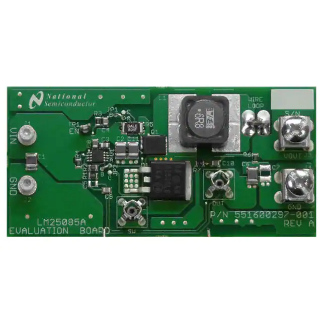
The LM25085AEVAL evaluation board provides the design engineer with a fully functional buck regulator,
employing the LM25085A PFET switching controller which uses the constant on-time (COT) operating
principle. This evaluation board provides a 1V output over an input range of 4.5V to 24V. The circuit
delivers load currents to 5A, with current limit set at ≊8.2A. The board is populated with all components
except C5 and C7.
The board’s specification are:
• Input Voltage: 4.5V to 24V
• Output Voltage: 1V
• Maximum load current: 5A
• Minimum load current: 0A
• Current Limit Threshold: ≊8.2A
• Measured Efficiency: 77.5% (VIN = 4.5V, IOUT = 1Amp, typical efficiency for converter providing a 1V
output)
• Nominal Switching Frequency: 200 kHz
• Size: 3.1 in. x 1.5 in.
Figure 1. Evaluation Board - Top Side
All trademarks are the property of their respective owners.
SNVA384B – February 2009 – Revised April 2013
Submit Documentation Feedback
AN-1933 LM25085A Evaluation Board
Copyright © 2009–2013, Texas Instruments Incorporated
1
�Theory of Operation
2
www.ti.com
Theory of Operation
Refer to the evaluation board schematic in Figure 6. When the circuit is in regulation, the on-time at the
PGATE output pin is determined by R4 and the voltage at VIN according to the equation:
-7
tON =
1.45 x 10 x (R4 + 1.4)
+ 50 ns
VIN ± 1.56V + R4/3167
(1)
where R4 is in kohms. The on-time at the SW node (junction of Q1, L1 and D1) is longer than the above
calculated on-time due to the difference of the turn-on and turn-off delay of Q1. The data sheet for the
Si7465 PFET indicates a typical turn-on delay of 8 ns, and a typical turn-off delay of 65 ns, resulting in an
additional 57 ns at the SW node. The SW on-time of this evaluation board ranges from ≊1209 ns at VIN =
4.5V, to ≊252 ns at VIN = 24V. The on-time varies inversely with VIN to maintain a nearly constant
switching frequency.
During the off-time, the load current is supplied by the inductor and the output capacitor (C6). When the
output voltage falls sufficiently that the voltage at FB is below the reference voltage (0.9V), the regulation
comparator initiates a new on-time period. For stable, fixed frequency operation, a minimum of 25 mV of
ripple is required at the FB pin to switch the regulation comparator. The required ripple is generated by R7
and C10, and supplied to the FB pin via C9.
The current limit threshold is set by the sense resistor (R5), and R3 at the ADJ pin, and is ≊8.2A on this
board. A current sink at the ADJ pin sets a constant voltage across R3. When the voltage across R5
exceeds the voltage across R3 the current limit comparator switches to shut off Q1, and the LM25085A
forces a longer-than-normal off-time. The long off-time is a function of the input voltage (VIN) and the
voltage at the FB pin, and is necessary to allow the inductor current to decrease at least as much, if not
more, than the current increase which occurred during the on-time.
The circuit may be shutdown at any time by grounding the Enable test point (EN, TP1). Removing the
ground connection allows normal operation to resume.
Refer to the LM25085A 42V Constant On-Time PFET Buck Switching Controller with 0.9V Reference
(SNVS601) data sheet for a detailed block diagram, and a complete description of the various functional
blocks.
3
Board Layout and Probing
The pictorial in Figure 1 shows the placement of the circuit components. The following should be kept in
mind when the board is powered:
• When operating at high load current forced air flow may be necessary to prevent overheating of Q1,
D1, and L1. These components may be hot to the touch.
• Use CAUTION when probing the circuit at high input voltages to prevent injury, as well as possible
damage to the circuit.
• At maximum load current (5A), the wire size and length used to connect the source voltage, and the
load, becomes important. Ensure there is not a significant drop in the wires supplying the input current
and the load current.
4
Board Connection/Start-up
The input connections are made to the J1 (+) and J2 (-) connectors. The load is connected to the J3
(VOUT) and J4 (GND) terminals. Ensure the wires are adequately sized for the intended load current.
Before start-up a voltmeter should be connected to the input terminals, and one to the output terminals.
The load current should be monitored with an ammeter or a current probe. It is recommended that the
input voltage be increased gradually to 4.5V, at which time the output voltage should be 1V. If the output
voltage is correct, then increase the input voltage as desired and proceed with evaluating the circuit. DO
NOT EXCEED 35V AT VIN.
2
AN-1933 LM25085A Evaluation Board
SNVA384B – February 2009 – Revised April 2013
Submit Documentation Feedback
Copyright © 2009–2013, Texas Instruments Incorporated
�Current Limit
www.ti.com
5
Current Limit
The LM25085A peak current limit detection operates by sensing the voltage across either the RDS(ON) of
Q1, or a sense resistor (R5), during the on-time and comparing it to the voltage across R3 at the ADJ pin.
The current limit threshold is reached when the sensed voltage exceeds the voltage across R3. When
current limit is reached Q1 is immediately switched off. The current limit function is much more accurate
and stable over temperature when a sense resistor is used. The RDS(ON) of a MOSFET has a wide process
variation and a large temperature coefficient.
Current sensing is disabled for a blanking time of ≊100 ns at the beginning of each on-time to prevent
false triggering of the current limit comparator due to leading edge current spikes. After Q1 is turned off
due to current limit detection, Q1 is held off for a longer-than-normal off-time. The extended off-time is a
function of the input voltage and the voltage at the FB pin, as shown below in the graph “Current Limit Offtime vs. VIN and VFB”. The current limit off-time can be calculated from the following:
-6
tOFF(CL) =
8 x 10 x ((VIN/31) + 0.15)
(VFB x 0.93) + 0.56V
(2)
The longer-than-normal forced off-time allows the inductor current to decrease to a low level before the
next on-time. This cycle-by-cycle monitoring, followed by a long forced off-time, provides effective
protection from output load faults over a wide range of operating conditions.
Figure 2. Current Limit Off-time vs. VIN and VFB
A) Sense resistor method – This evaluation board is supplied configured for the sense resistor method
of current limit detection. Jumpers A-B are in place at both jumper locations (JP1, JP2), which connects
the ADJ pin resistor (R3) and the ISEN pin across the sense resistor (R5). If the voltage across R5
exceeds the voltage across R3 during the on-time, the current limit comparator switches to turn off Q1.
The voltage across R3 is set by an internal 40 µA current sink at the ADJ pin. The current at which the
current limit comparator switches is calculated from:
ICL = 40 µA x R3/R5
(3)
With R5 = 10 mΩ and R3 = 2.05 kΩ, the nominal current limit threshold calculates to 8.2A. Since that is
the peak of the inductor current waveform, the load current is equal to that peak value minus one half the
ripple current amplitude. At Vin = 4.5V, the ripple amplitude is ≊622 mAp-p, and the load current at current
limit is equal to 7.89A. At Vin = 24V, the ripple amplitude is ≊851 mAp-p, and the load current at current
limit is equal to ≊7.77A.
Using the tolerances for the ADJ pin current and the current limit comparator offset, the maximum current
limit threshold calculates to:
ICL(max) =
(2.05 k: x 48 PA) + 9 mV
0.01:
= 10.74A
(4)
and the load current at current limit calculates to 10.43A at 4.5V, and 10.32A at 24V. The minimum
current limit thresholds calculate to:
ICL(min) =
(2.05 k: x 32 PA) - 9 mV
0.01:
= 5.66A
(5)
SNVA384B – February 2009 – Revised April 2013
Submit Documentation Feedback
AN-1933 LM25085A Evaluation Board
Copyright © 2009–2013, Texas Instruments Incorporated
3
�Output Ripple Control
www.ti.com
and the load current at current limit calculates to 5.35A at 4.5V, and 5.24A at 24V.
To change the current limit threshold the value for R5 should be chosen to achieve 50 mV to 100 mV
across it at current limit, staying within the practical limitations of power dissipation and physical size of the
resistor. A larger value for R5 reduces the effects of the current limit comparator offset, but at the expense
of higher power dissipation. After selecting the value for R5, calculate the value for R3 by rearranging
Equation 1 above. See the Applications Information section of the LM25085A data sheet for a procedure
to account for ripple current amplitude and tolerances when selecting the resistor for the ADJ pin.
B) Q1 RDS(ON) method – To configure the evaluation board to use the RDS(ON) of Q1 for current limit
detection, move the jumpers at both JP1 and JP2 from the A-B position to the B-C position. This change
connects the ADJ pin resistor (R3) and the ISEN pin across Q1. Since the sense resistance is now the
RDS(ON) of Q1, R3 must be changed. The data sheet for the Si7465 PFET lists the typical RDS(ON) as 51 mΩ
at VGS = 10V, and 64 mΩ at VGS = 4.5V. Therefore, the RDS(ON) is estimated to be nominally 57 mΩ at VGS =
7.7V. To achieve the same nominal current limit threshold as above (8.2A), using Equation 6 in the data
sheet R3 calculates to:
R3 =
8.2A x 0.057:
40 PA
= 11.7 k:
(6)
The load current is equal to the current limit threshold minus half the current ripple amplitude. R3 can be
changed to set other current limit detection thresholds.
6
Output Ripple Control
The LM25085A requires a minimum of 25 mVp-p ripple at the FB pin, in phase with the switching
waveform at the SW node, for proper operation. On this evaluation board, the required ripple is generated
by R7, C9, and C10, allowing the ripple at VOUT to be kept to a minimum, as described in option A below.
Alternatively, the required ripple at the FB pin can be supplied from ripple generated at VOUT and passed
through the feedback resistors, as described in options B and C below, using one or two less external
components.
A) Minimum Output Ripple: This evaluation board is supplied configured for minimum ripple at VOUT by
using components R7, C9 and C10. The ripple voltage required by the FB pin is generated by R7 and C10
since the SW node switches from ≊-1V to VIN, and the right end of C10 is a virtual ground. The values for
R7 and C10 are chosen to generate a 25-40 mVp-p triangle waveform at their junction. That triangle wave
is then coupled to the FB pin through C9. The following procedure is used to calculate values for R7, C9
and C10:
1) Calculate the voltage VA:
VA = VOUT - (VSW x (1 - (VOUT/VIN(min))))
(7)
where VSW is the absolute value of the voltage at the SW node during the off-time, typically 0.5V to 1V
depending on the diode, and VIN is the minimum input voltage. Using a typical value of 0.65V for VSW, VA
calculates to 0.49V. This is the approximate DC voltage at the R7/C10 junction, and is used in the next
equation.
2) Calculate the R7xC10 product:
R7 x C10 =
(VIN - VA) x tON
'V
(8)
where tON is the maximum on-time (≊1209 ns), VIN is the minimum input voltage, and ΔV is the desired
ripple amplitude at the R7/C10 junction, 30 mVp-p for this example.
R7 x C10 =
(4.5V ± 0.49V) x 1209 ns
-5
= 16.2 x 10
0.03V
(9)
R7 and C10 are then chosen from standard value components to satisfy the above product. On this
evaluation board, C10 is set at 3300 pF. R7 calculate to be 49 kΩ, and a standard value 48.7 kΩ resistor
is used. C9 is chosen to be 0.01 µF, large compared to C10. The circuit as supplied on this EVB is shown
in Figure 3.
The output ripple, which ranges from ≊20 mVp-p at VIN = 4.5V to ≊33 mVp-p at VIN = 24V, is determined
primarily by the ESR of the output capacitance (C6), and the inductor’s ripple current. See Figure 10.
4
AN-1933 LM25085A Evaluation Board
SNVA384B – February 2009 – Revised April 2013
Submit Documentation Feedback
Copyright © 2009–2013, Texas Instruments Incorporated
�Output Ripple Control
www.ti.com
LM25085A
PGATE
Q1
L1 6.8 PH
Pads for
wire loop
VOUT
1V
D1
GND
FB
R1
1.1k
C10
3300 pF
R7
48.7k
C9
0.01 PF
R6
0:
C6
68 PF
R2
10k
GND
Figure 3. Minimum Ripple Using R7, C9, C10
B) Reduced Ripple Level Configuration: This configuration generates more ripple at VOUT than the
above configuration, but uses one less capacitor. If some ripple is acceptable in the application, this
configuration is slightly more economical, and simpler. R6 and C5 are used instead of R7, C9 and C10, as
shown in Figure 4.
Ripple is generated at VOUT as the inductor’s ripple current flows through R6, and that ripple voltage is
passed to the FB pin via C5. The ripple at VOUT can be set as low as 25 mVp-p since it is not attenuated
by R1 and R2. The minimum value for R6 is calculated from:
(10)
where IOR(min) is the minimum inductor’s ripple current, which occurs at minimum input voltage, and is 622
mAp-p at 4.5V. The minimum value for R6 calculates to 0.04 ohms. Using a standard value 43 mΩ
resistor for R6, the ripple at VOUT ranges from 27 mVp-p to 37 mVp-p over the input voltage range. See
Figure 10.
The minimum value for C5 is determined from:
(11)
Where tON(max) is the maximum on-time, 1209 ns in this evaluation board. The minimum value for C5
calculates to 3660 pF.
LM25085A
PGATE
Q1
L1 6.8 PH
Pads for
wire loop
VOUT
1V
D1
GND
C5
3900 pF
R1
1.1k
R6
0.043:
FB
C6
68 PF
R2
10k
GND
Figure 4. Reduced Ripple Configuration
SNVA384B – February 2009 – Revised April 2013
Submit Documentation Feedback
AN-1933 LM25085A Evaluation Board
Copyright © 2009–2013, Texas Instruments Incorporated
5
�Monitor The Inductor Current
www.ti.com
C) Lowest Cost Configuration: This configuration is the same as option B above, but with C5 removed.
The ripple at the FB pin is attenuated from that at VOUT by the feedback resistors (R1, R2). Since ≥25
mVp-p are required at the FB pin, R6 is chosen to generate ≥28 mV at VOUT. Since the minimum ripple
current in this circuit is 622 mAp-p the minimum value for R6 calculates to 45 mΩ. Using a standard value
51 mΩ resistor for R6, the ripple at VOUT ranges from ≊32 mVp-p to ≊43 mVp-p over the input voltage
range. See Figure 10. If the application can accept this ripple level, this is the most economical solution.
The circuit is shown in Figure 5.
LM25085A
PGATE
Q1
L1 6.8 PH
Pads for
wire loop
VOUT
1V
D1
GND
R6
0.051:
R1
1.1k
FB
C6
68 PF
R2
10k
GND
Figure 5. Lowest Cost Configuration
7
Monitor The Inductor Current
The inductor’s current can be monitored or viewed on a scope with a current probe. Remove the jumper
from the WIRE LOOP pads, and install an appropriate current loop across the pads. In this way the
inductor’s ripple current and peak current can be accurately determined.
8
Scope Probe Adapters
Scope probe adapters are provided on this evaluation board for monitoring the waveform at the SW node,
and at the circuit’s output (VOUT), without using the probe’s ground lead which can pick up noise from the
switching waveforms. The probe adapters are suitable for Tektronix P6137 or similar probes, with a 0.135”
diameter.
4.5V to 24V
Input
VIN
C1
10 PF
C3
0.47 PF
VCC
C2
10 PF
C11
VIN
C8
0.1 PF
LM25085A
JP1 A
B
C
R3 2.05k
R4
21k
ISEN
RT
ENABLE
1000 pF
ADJ
10 PF
GND
C4
PGATE
JP2
B
R5
10 m:
A
C
Q1
TP1
Pads for
wire loop
L1 6.8 PH
VOUT
1V
SW
D1
GND
FB
R7
48.7k
C9
0.01 PF
R6
0:
R1
1.1k
C10
3300 pF C5
VOUT
R2
10k
C6
68 PF
C7
GND
Figure 6. Complete Evaluation Board Schematic
6
AN-1933 LM25085A Evaluation Board
SNVA384B – February 2009 – Revised April 2013
Submit Documentation Feedback
Copyright © 2009–2013, Texas Instruments Incorporated
�Bill of Materials
www.ti.com
9
Bill of Materials
Table 1. Bill of Materials
Item
Description
Mfg., Part Number
Package
Value
C1, C2, C11
Ceramic Capacitor
Taiyo Yuden
GMK325BJ106KN
1210
10 µF, 35V
C3
Ceramic Capacitor
TDK C2012X7R1C474K
0805
0.47 µF, 16V
C4
Ceramic Capacitor
TDK C2012X7R2A102K
0805
1000 pF, 100V
Unpopulated
0805
Ceramic Capacitor
TDK C3225X5R0J686M
1210
C5
C6
C7
68 µF, 6.3V
Unpopulated
C8
Ceramic Capacitor
TDK C2012X7R2A104K
0805
0.1 µF, 100V
C9
Ceramic Capacitor
TDK C2012X7R2A103K
0805
0.01 µF, 100V
C10
Ceramic Capacitor
TKD C2012X7R2A332K
0805
3300 pF, 100V
D1
Schottky Diode
On Semi
MBRB2535CTL
D2PAK
35V, 25A
L1
Power Inductor
Wurth XXL 7447709006
12 mm x 12 mm
6.8 µH
Q1
P-Channel MOSFET
Vishay Si7465DP
SO-8 Power
60V, 5A
R1
Resistor
Vishay
CRCW08051101F
0805
1.1k
R2
Resistor
Vishay
CRCW08051002F
0805
10k
R3
Resistor
Vishay
CRCW08052051F
0805
2.05k
R4
Resistor
Vishay
CRCW08052102F
0805
21k
R5
Resistor
Vishay
WSL2010R0100F
2010
0.01 ohm,
R6
Resistor
Vishay
CRCW08050000Z
0805
0 ohms
R7
Resistor
Vishay
CRCW08054872F
0805
48.7k
U1
Switching Regulator
LM25085
VSSOP8-EP
SNVA384B – February 2009 – Revised April 2013
Submit Documentation Feedback
AN-1933 LM25085A Evaluation Board
Copyright © 2009–2013, Texas Instruments Incorporated
7
�Circuit Performance
10
www.ti.com
Circuit Performance
(Efficiencies in this range are typical for a buck converter producing a 1.0V output)
Figure 7. Efficiency vs Load Current
Figure 8. Efficiency vs Input Voltage
Figure 9. Switching Frequency vs. Input Voltage
8
AN-1933 LM25085A Evaluation Board
SNVA384B – February 2009 – Revised April 2013
Submit Documentation Feedback
Copyright © 2009–2013, Texas Instruments Incorporated
�Circuit Performance
www.ti.com
Figure 10. Output Voltage Ripple
Figure 11. Line Regulation
Figure 12. Load Regulation
SNVA384B – February 2009 – Revised April 2013
Submit Documentation Feedback
AN-1933 LM25085A Evaluation Board
Copyright © 2009–2013, Texas Instruments Incorporated
9
�Typical Waveforms
11
www.ti.com
Typical Waveforms
Trace 4 = Inductor Current
Trace 3 = VOUT
Trace 1 = SW Node
VIN = 12V, IOUT = 1Amp
Minimum Ripple Configuration (Option A)
Figure 13. Continuous Conduction Mode
Trace 4 = Inductor Current
Trace 3 = VOUT
Trace 1 = SW Node
VIN = 12V, IOUT = 0
Figure 14. Discontinuous Conduction Mode
Trace 4 = Inductor Current
Trace 3 = VOUT
Trace 1 = SW Node
VIN = 12V, IOUT = 0
Figure 15. Discontinuous Conduction Mode (Expanded Scale)
10
AN-1933 LM25085A Evaluation Board
SNVA384B – February 2009 – Revised April 2013
Submit Documentation Feedback
Copyright © 2009–2013, Texas Instruments Incorporated
�PC Board Layout
www.ti.com
12
PC Board Layout
Figure 16. Board Silkscreen
Figure 17. Board Top Layer
Figure 18. Board Bottom Layer (Viewed from Top)
SNVA384B – February 2009 – Revised April 2013
Submit Documentation Feedback
AN-1933 LM25085A Evaluation Board
Copyright © 2009–2013, Texas Instruments Incorporated
11
�IMPORTANT NOTICE
Texas Instruments Incorporated and its subsidiaries (TI) reserve the right to make corrections, enhancements, improvements and other
changes to its semiconductor products and services per JESD46, latest issue, and to discontinue any product or service per JESD48, latest
issue. Buyers should obtain the latest relevant information before placing orders and should verify that such information is current and
complete. All semiconductor products (also referred to herein as “components”) are sold subject to TI’s terms and conditions of sale
supplied at the time of order acknowledgment.
TI warrants performance of its components to the specifications applicable at the time of sale, in accordance with the warranty in TI’s terms
and conditions of sale of semiconductor products. Testing and other quality control techniques are used to the extent TI deems necessary
to support this warranty. Except where mandated by applicable law, testing of all parameters of each component is not necessarily
performed.
TI assumes no liability for applications assistance or the design of Buyers’ products. Buyers are responsible for their products and
applications using TI components. To minimize the risks associated with Buyers’ products and applications, Buyers should provide
adequate design and operating safeguards.
TI does not warrant or represent that any license, either express or implied, is granted under any patent right, copyright, mask work right, or
other intellectual property right relating to any combination, machine, or process in which TI components or services are used. Information
published by TI regarding third-party products or services does not constitute a license to use such products or services or a warranty or
endorsement thereof. Use of such information may require a license from a third party under the patents or other intellectual property of the
third party, or a license from TI under the patents or other intellectual property of TI.
Reproduction of significant portions of TI information in TI data books or data sheets is permissible only if reproduction is without alteration
and is accompanied by all associated warranties, conditions, limitations, and notices. TI is not responsible or liable for such altered
documentation. Information of third parties may be subject to additional restrictions.
Resale of TI components or services with statements different from or beyond the parameters stated by TI for that component or service
voids all express and any implied warranties for the associated TI component or service and is an unfair and deceptive business practice.
TI is not responsible or liable for any such statements.
Buyer acknowledges and agrees that it is solely responsible for compliance with all legal, regulatory and safety-related requirements
concerning its products, and any use of TI components in its applications, notwithstanding any applications-related information or support
that may be provided by TI. Buyer represents and agrees that it has all the necessary expertise to create and implement safeguards which
anticipate dangerous consequences of failures, monitor failures and their consequences, lessen the likelihood of failures that might cause
harm and take appropriate remedial actions. Buyer will fully indemnify TI and its representatives against any damages arising out of the use
of any TI components in safety-critical applications.
In some cases, TI components may be promoted specifically to facilitate safety-related applications. With such components, TI’s goal is to
help enable customers to design and create their own end-product solutions that meet applicable functional safety standards and
requirements. Nonetheless, such components are subject to these terms.
No TI components are authorized for use in FDA Class III (or similar life-critical medical equipment) unless authorized officers of the parties
have executed a special agreement specifically governing such use.
Only those TI components which TI has specifically designated as military grade or “enhanced plastic” are designed and intended for use in
military/aerospace applications or environments. Buyer acknowledges and agrees that any military or aerospace use of TI components
which have not been so designated is solely at the Buyer's risk, and that Buyer is solely responsible for compliance with all legal and
regulatory requirements in connection with such use.
TI has specifically designated certain components as meeting ISO/TS16949 requirements, mainly for automotive use. In any case of use of
non-designated products, TI will not be responsible for any failure to meet ISO/TS16949.
Products
Applications
Audio
www.ti.com/audio
Automotive and Transportation
www.ti.com/automotive
Amplifiers
amplifier.ti.com
Communications and Telecom
www.ti.com/communications
Data Converters
dataconverter.ti.com
Computers and Peripherals
www.ti.com/computers
DLP® Products
www.dlp.com
Consumer Electronics
www.ti.com/consumer-apps
DSP
dsp.ti.com
Energy and Lighting
www.ti.com/energy
Clocks and Timers
www.ti.com/clocks
Industrial
www.ti.com/industrial
Interface
interface.ti.com
Medical
www.ti.com/medical
Logic
logic.ti.com
Security
www.ti.com/security
Power Mgmt
power.ti.com
Space, Avionics and Defense
www.ti.com/space-avionics-defense
Microcontrollers
microcontroller.ti.com
Video and Imaging
www.ti.com/video
RFID
www.ti-rfid.com
OMAP Applications Processors
www.ti.com/omap
TI E2E Community
e2e.ti.com
Wireless Connectivity
www.ti.com/wirelessconnectivity
Mailing Address: Texas Instruments, Post Office Box 655303, Dallas, Texas 75265
Copyright © 2013, Texas Instruments Incorporated
�