User's Guide
SNVA102A – October 2005 – Revised April 2013
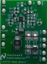
AN —1356 LM2743 Evaluation Board
1
Introduction
This application notes describes the LM2743 printed circuit board (PCB) design and provides an example
typical application circuit. The demo board allows component design flexibility in order to demonstrate the
versatility of the LM2743 IC.
The demo board contains a voltage-mode, high-speed synchronous buck regulator controller. Though the
control sections of the IC are rated for 3 to 6V (VCC), the driver sections are designed to accept input
supply rails (VIN) as high as 14V.
The demo board design regulates to an output voltage of 1.2V at 3.5A with a switching frequency of
1MHz. Note, the demo board is optimized for a 1MHz, 14V input voltage compensation design, if another
switching frequency and input voltage is desired, please consult the LM2743 data sheet for control loop
compensation procedures. For additional design modifications refer to the Design Consideration section of
the LM2743 Low Voltage N-Channel MOSFET Synchronous Buck Regulator Controller Data Sheet
(SNVS276). The PCB is designed on two layers with 1oz. copper on a 62mil FR4 laminate.
2
Additional Footprints
A Schottky diode footprint (D1) is available in parallel to the low side MOSFET. This component can
improve efficiency, due to the lower forward drop than the low side MOSFET body diode conducting
during the anti-shoot through period. Select a Schottky diode that maintains a forward drop around 0.4 to
0.6V at the maximum load current (consult the I-V curve). In addition select the reverse breakdown
voltage to have sufficient margin above the maximum input voltage.
Footprint C13 is available for a multilayer ceramic capacitor (MLCC) connected as close as possible to the
source of the low side MOSFET and drain of the high side MOSFET. This will provide low supply
impedance to the high speed switch currents, thus minimizing the input supply noise. For example; a
MLCC is used (C13) in combination with aluminum electrolytic input filter capacitors, placed in designators
C12 and C14, because MLCC have lower impedance than electrolytics. If MLCCs are used in designators
C12 and C14 then component C13 is not necessary.
3
Typical Application Circuit
The typical application circuit in Figure 1 provides the component designators used on the demo board.
All trademarks are the property of their respective owners.
SNVA102A – October 2005 – Revised April 2013
Submit Documentation Feedback
AN —1356 LM2743 Evaluation Board
Copyright © 2005–2013, Texas Instruments Incorporated
1
�Typical Application Circuit
www.ti.com
VC
D2
C
R11
R8
R1
J1
C5
C12
HG
VCC
SD
BOOT
PWGD
C14
Q1
VOUT
L1
R4
ISEN
LM2743
FREQ
R2
C7
VIN
C10
LG
SS/TRACK
PGND
SGND
PGND
+
Q2
C16
FB
EAO
C9
R3
R5
C11
R6
C8
R7
Figure 1. Typical Application
2
AN —1356 LM2743 Evaluation Board
SNVA102A – October 2005 – Revised April 2013
Submit Documentation Feedback
Copyright © 2005–2013, Texas Instruments Incorporated
�Performance Characteristics
www.ti.com
4
Performance Characteristics
4.1
Switch Node Voltage and Output Ripple Voltage
Figure 2. VIN = VCC = 3.3V,
VOUT = 1.2V,
ILOAD = 0A, fSW = 1MHz.
20 MHz Bandwidth Limit
Figure 3. VIN = VCC = 3.3V,
VOUT = 1.2V,
ILOAD = 3.5A, fSW = 1MHz.
20 MHz Bandwidth Limit
Figure 4. VIN = 14V, VCC = 5V,
VOUT = 1.2V, ILOAD = 0A, fSW = 1MHz.
20 MHz Bandwidth Limit
Figure 5. VIN = 14V, VCC = 5V,
VOUT = 1.2V, ILOAD = 3.5A, fSW = 1MHz.
20 MHz Bandwidth Limit
SNVA102A – October 2005 – Revised April 2013
Submit Documentation Feedback
AN —1356 LM2743 Evaluation Board
Copyright © 2005–2013, Texas Instruments Incorporated
3
�Performance Characteristics
www.ti.com
Table 1. Bill of Materials
Designator
Function
Part Description
Part Number
U1
Controller
IC LM2743 TSSOP14
Texas Instruments
C5
VCC Decoupling
Cer Cap 1µF 25V 10% 0805
Murata GRM216R61E105KA12B
C7
Soft Start Cap
Cer Cap 12nF 25V 10% 0805
Vishay VJ0805Y123KXX
C8
Comp Cap
Cer Cap 1.5nF 25V 10% 0805
Vishay VJ0805Y152KXX
C9
Comp Cap
Cer Cap 18pF 25V 10% 0805
Vishay VJ0805A180KAA
C10
Cboot
Cer Cap 0.1µF 25V 10% 0805
Vishay VJ0805Y104KXX
C11
Comp Cap
Cer Cap 1.8nF 25V 10% 0805
Vishay VJ0805Y182KXX
C12
Input Filter Cap
Cer Cap 10uF 25V 10% 1210
AVX 12103D106MAT
C14
Input Filter Cap
Cer Cap 10uF 25V 10% 1210
AVX 12103D106MAT
C15
Output Filter Cap
470µF, 6.3V, 10mΩ ESR POScap
Sanyo 6TPD470
R1
Filter Resistor
Res 10Ω .25W 0805
Vishay CRCW08051000F
R2
Frequency Adjust Res
Res 24.9KΩ .25W 0805
Vishay CRCW08052492F
R3
Comp Res
Res 17.4KΩ .25W 0805
Vishay CRCW08051742F
R4
Current Limit Res
Res 3.16KΩ .25W 0805
Vishay CRCW08053161F
R5
Comp Res
Res 2.94KΩ .25W 0805
Vishay CRCW08052941F
R6
Res Divider, upper
Res 10.0KΩ .25W 0805
Vishay CRCW08051002F
R7
Res Divider, lower
Res 10.0KΩ .25W 0805
Vishay CRCW08051002F
R8
PWGD Pull-Up
Res 100KΩ .25W 0805
Vishay CRCW08051003F
R11
Shut Down Pull-Up
Res 100KΩ .25W 0805
Vishay CRCW080561003F
D2
Bootstrap Diode
Schottky Diode, SOD-123
MBR0530LTI
L1
Output Filter Inductor
Inductor 1µH, 5.3Arms, 10.2mΩ
Cooper DR73-1R0
Q1-Q2
Top and Bottom FETs
Dual N-MOSFET, VDS = 20V, 24mΩ @ 2.5V
Vishay 9926BDY
VC
D2
C
R1
R11
R8
C13
VCC
J1
C5
HG
SD
BOOT
PWGD
FREQ
R2
C7
VIN
C10
C12
C14
Q1
VOUT
L1
R4
ISEN
LM2743
LG
SS/TRACK
PGND
SGND
PGND
D1
Q2
C15
+
+
C16
FB
EAO
C9
R3
R5
C11
R6
C8
R7
Figure 6. Complete Demo Board Schematic
4
AN —1356 LM2743 Evaluation Board
SNVA102A – October 2005 – Revised April 2013
Submit Documentation Feedback
Copyright © 2005–2013, Texas Instruments Incorporated
�PCB Layout Diagram(s)
www.ti.com
5
PCB Layout Diagram(s)
Figure 7. Top Layer and Top Overlay
Figure 8. Bottom Layer
SNVA102A – October 2005 – Revised April 2013
Submit Documentation Feedback
AN —1356 LM2743 Evaluation Board
Copyright © 2005–2013, Texas Instruments Incorporated
5
�IMPORTANT NOTICE
Texas Instruments Incorporated and its subsidiaries (TI) reserve the right to make corrections, enhancements, improvements and other
changes to its semiconductor products and services per JESD46, latest issue, and to discontinue any product or service per JESD48, latest
issue. Buyers should obtain the latest relevant information before placing orders and should verify that such information is current and
complete. All semiconductor products (also referred to herein as “components”) are sold subject to TI’s terms and conditions of sale
supplied at the time of order acknowledgment.
TI warrants performance of its components to the specifications applicable at the time of sale, in accordance with the warranty in TI’s terms
and conditions of sale of semiconductor products. Testing and other quality control techniques are used to the extent TI deems necessary
to support this warranty. Except where mandated by applicable law, testing of all parameters of each component is not necessarily
performed.
TI assumes no liability for applications assistance or the design of Buyers’ products. Buyers are responsible for their products and
applications using TI components. To minimize the risks associated with Buyers’ products and applications, Buyers should provide
adequate design and operating safeguards.
TI does not warrant or represent that any license, either express or implied, is granted under any patent right, copyright, mask work right, or
other intellectual property right relating to any combination, machine, or process in which TI components or services are used. Information
published by TI regarding third-party products or services does not constitute a license to use such products or services or a warranty or
endorsement thereof. Use of such information may require a license from a third party under the patents or other intellectual property of the
third party, or a license from TI under the patents or other intellectual property of TI.
Reproduction of significant portions of TI information in TI data books or data sheets is permissible only if reproduction is without alteration
and is accompanied by all associated warranties, conditions, limitations, and notices. TI is not responsible or liable for such altered
documentation. Information of third parties may be subject to additional restrictions.
Resale of TI components or services with statements different from or beyond the parameters stated by TI for that component or service
voids all express and any implied warranties for the associated TI component or service and is an unfair and deceptive business practice.
TI is not responsible or liable for any such statements.
Buyer acknowledges and agrees that it is solely responsible for compliance with all legal, regulatory and safety-related requirements
concerning its products, and any use of TI components in its applications, notwithstanding any applications-related information or support
that may be provided by TI. Buyer represents and agrees that it has all the necessary expertise to create and implement safeguards which
anticipate dangerous consequences of failures, monitor failures and their consequences, lessen the likelihood of failures that might cause
harm and take appropriate remedial actions. Buyer will fully indemnify TI and its representatives against any damages arising out of the use
of any TI components in safety-critical applications.
In some cases, TI components may be promoted specifically to facilitate safety-related applications. With such components, TI’s goal is to
help enable customers to design and create their own end-product solutions that meet applicable functional safety standards and
requirements. Nonetheless, such components are subject to these terms.
No TI components are authorized for use in FDA Class III (or similar life-critical medical equipment) unless authorized officers of the parties
have executed a special agreement specifically governing such use.
Only those TI components which TI has specifically designated as military grade or “enhanced plastic” are designed and intended for use in
military/aerospace applications or environments. Buyer acknowledges and agrees that any military or aerospace use of TI components
which have not been so designated is solely at the Buyer's risk, and that Buyer is solely responsible for compliance with all legal and
regulatory requirements in connection with such use.
TI has specifically designated certain components as meeting ISO/TS16949 requirements, mainly for automotive use. In any case of use of
non-designated products, TI will not be responsible for any failure to meet ISO/TS16949.
Products
Applications
Audio
www.ti.com/audio
Automotive and Transportation
www.ti.com/automotive
Amplifiers
amplifier.ti.com
Communications and Telecom
www.ti.com/communications
Data Converters
dataconverter.ti.com
Computers and Peripherals
www.ti.com/computers
DLP® Products
www.dlp.com
Consumer Electronics
www.ti.com/consumer-apps
DSP
dsp.ti.com
Energy and Lighting
www.ti.com/energy
Clocks and Timers
www.ti.com/clocks
Industrial
www.ti.com/industrial
Interface
interface.ti.com
Medical
www.ti.com/medical
Logic
logic.ti.com
Security
www.ti.com/security
Power Mgmt
power.ti.com
Space, Avionics and Defense
www.ti.com/space-avionics-defense
Microcontrollers
microcontroller.ti.com
Video and Imaging
www.ti.com/video
RFID
www.ti-rfid.com
OMAP Applications Processors
www.ti.com/omap
TI E2E Community
e2e.ti.com
Wireless Connectivity
www.ti.com/wirelessconnectivity
Mailing Address: Texas Instruments, Post Office Box 655303, Dallas, Texas 75265
Copyright © 2013, Texas Instruments Incorporated
�