Product
Folder
Order
Now
Support &
Community
Tools &
Software
Technical
Documents
LM317
SLVS044Y – SEPTEMBER 1997 – REVISED APRIL 2020
LM317 3-Terminal Adjustable Regulator
1 Features
3 Description
•
The LM317 device is an adjustable three-terminal
positive-voltage regulator capable of supplying more
than 1.5 A over an output-voltage range of 1.25 V to
37 V. It requires only two external resistors to set the
output voltage. The device features a typical line
regulation of 0.01% and typical load regulation of
0.1%. It includes current limiting, thermal overload
protection, and safe operating area protection.
Overload protection remains functional even if the
ADJUST terminal is disconnected.
1
•
•
•
•
Output voltage range adjustable
from 1.25 V to 37 V
Output current greater than 1.5 A
Internal short-circuit current limiting
Thermal overload protection
Output safe-area compensation
2 Applications
•
•
•
•
•
•
•
•
•
•
•
•
•
•
•
•
•
•
•
•
•
•
•
•
•
•
•
•
•
•
•
•
ATCA solutions
DLP: 3D biometrics, hyperspectral imaging,
optical networking, and spectroscopy
DVR and DVS
Desktop PCs
Digital signage and still cameras
ECG electrocardiograms
EV HEV chargers: levels 1, 2, and 3
Electronic shelf labels
Energy harvesting
Ethernet switches
Femto base stations
Fingerprint and iris biometrics
HVAC: heating, ventilating, and air conditioning
High-speed data acquisition and generation
Hydraulic valves
IP phones: wired and wireless
Intelligent occupancy sensing
Motor controls: brushed DC, brushless DC, lowvoltage, permanent magnet, and stepper motors
Point-to-point microwave backhauls
Power bank solutions
Power line communication modems
Power over ethernet (PoE)
Power quality meters
Power substation controls
Private branch exchanges (PBX)
Programmable logic controllers
RFID readers
Refrigerators
Signal or waveform generators
Software-defined radios (SDR)
Washing machines: high-end and low-end
X-rays: baggage scanners, medical, and dental
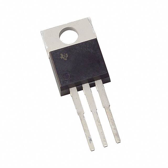
Device Information(1)
PART NUMBER
PACKAGE
BODY SIZE (NOM)
LM317DCY
SOT-223 (4)
6.50 mm × 3.50 mm
LM317KCS
TO-220 (3)
10.16 mm × 9.15 mm
LM317KCT
TO-220 (3)
10.16 mm × 8.59 mm
LM317KTT
TO-263 (3)
10.16 mm × 9.01 mm
(1) For all available packages, see the orderable addendum at
the end of the data sheet.
Battery-Charger Circuit
LM317
VI
INPUT
RS
0.2 W
OUTPUT
ADJUST
R1
240 W
R2
2.4 kW
1
An IMPORTANT NOTICE at the end of this data sheet addresses availability, warranty, changes, use in safety-critical applications,
intellectual property matters and other important disclaimers. PRODUCTION DATA.
�LM317
SLVS044Y – SEPTEMBER 1997 – REVISED APRIL 2020
www.ti.com
Table of Contents
1
2
3
4
5
6
7
8
Features ..................................................................
Applications ...........................................................
Description .............................................................
Revision History.....................................................
Device Comparison Table.....................................
Pin Configuration and Functions .........................
Specifications.........................................................
1
1
1
2
3
4
5
7.1
7.2
7.3
7.4
7.5
7.6
5
5
5
5
6
7
Absolute Maximum Ratings ......................................
ESD Ratings..............................................................
Recommended Operating Conditions.......................
Thermal Information ..................................................
Electrical Characteristics...........................................
Typical Characteristics ..............................................
Detailed Description .............................................. 9
8.1 Overview ................................................................... 9
8.2 Functional Block Diagram ......................................... 9
8.3 Feature Description................................................... 9
8.4 Device Functional Modes........................................ 10
9
Application and Implementation ........................ 11
9.1 Application Information............................................ 11
9.2 Typical Application .................................................. 11
9.3 System Examples ................................................... 12
10 Power Supply Recommendations ..................... 18
11 Layout................................................................... 18
11.1 Layout Guidelines ................................................. 18
11.2 Layout Example .................................................... 18
12 Device and Documentation Support ................. 19
12.1
12.2
12.3
12.4
12.5
Receiving Notification of Documentation Updates
Support Resources ...............................................
Trademarks ...........................................................
Electrostatic Discharge Caution ............................
Glossary ................................................................
19
19
19
19
19
13 Mechanical, Packaging, and Orderable
Information ........................................................... 19
4 Revision History
Changes from Revision X (September 2016) to Revision Y
Page
•
Added Device Comparison Table .......................................................................................................................................... 3
•
Changed VIN to IOUT in Load Transient Response figures ...................................................................................................... 7
•
Added missing caption to second y-axis in second Load Transient Response figure ........................................................... 7
•
Changed VOUT and output impedance equations in Battery-Charger Circuit section........................................................... 14
Changes from Revision W (January 2015) to Revision X
Page
•
Changed body size dimensions for KCS TO-220 Package on Device information table ...................................................... 1
•
Changed body size dimensions for KTT TO-263 Package on Device information table ...................................................... 1
•
Changed VO Output Voltage max value from 7 to 37 on Recommended Operating Conditions table .................................. 5
•
Added min value to IO Output Current in Recommended Operating Conditions table .......................................................... 5
•
Changed values in the Thermal Information table to align with JEDEC standards ............................................................... 5
•
Added KCT package data to Thermal Information table ....................................................................................................... 5
•
Deleted Section 9.3.6 "Adjusting Multiple On-Card Regulators with a Single Control" ....................................................... 14
•
Updated Adjustsable 4-A Regulator Circuit graphic ............................................................................................................ 16
•
Added Receiving Notification of Documentation Updates section and Community Resources section .............................. 19
Changes from Revision V (February 2013) to Revision W
Page
•
Added Applications, Device Information table, Pin Functions table, ESD Ratings table, Thermal Information table,
Feature Description section, Device Functional Modes, Application and Implementation section, Power Supply
Recommendations section, Layout section, Device and Documentation Support section, and Mechanical,
Packaging, and Orderable Information section. ..................................................................................................................... 1
•
Deleted Ordering Information table. ....................................................................................................................................... 1
2
Submit Documentation Feedback
Copyright © 1997–2020, Texas Instruments Incorporated
Product Folder Links: LM317
�LM317
www.ti.com
SLVS044Y – SEPTEMBER 1997 – REVISED APRIL 2020
5 Device Comparison Table
IOUT
1.5 A
PARAMETER
LM317
LM317-N
LM317A
LM317HV
Input voltage range
4.25 - 40
4.25 - 40
4.25 - 40
4.25 - 60
UNIT
V
Load regulation accuracy
1.5
1.5
1
1.5
%
dB
PSRR (120 Hz)
64
80
80
65
Recommended operating temperature
0 to 125
0 to 125
–40 to 125
0 to 125
°C
TO-220 (NDE) TJA
23.5
23.2
23.3
23
°C/W
TO-200 (KCT) TJA
37.9
N/A
N/A
°C/W
TO-252 TJA
N/A
54
54
°C/W
TO-263 TJA
38
41
N/A
°C/W
SOT-223 TJA
66.8
59.6
59.6
°C/W
N/A
186
186
°C/W
TO-92 TJA
LM317M
0.5 A
Input voltage range
3.75 - 40
Load regulation accuracy
1.5
%
PSRR (120 Hz)
80
dB
Recommended operating temperature
-40 - 125
°C
SOT-223 TJA
60.2
°C/W
TO-252 TJA
56.9
°C/W
LM317L
LM317L-N
3.75 - 40
4.25 - 40
Load regulation accuracy
1
1.5
%
PSRR (120 Hz)
62
80
dB
Recommended operating temperature
–40 to 125
–40 to 125
°C
SOT-23 TJA
167.8
N/A
°C/W
SO-8 TJA
N/A
165
°C/W
DSBGA TJA
N/A
290
°C/W
TO-92 TJA
N/A
180
°C/W
Input voltage range
0.1 A
V
V
Submit Documentation Feedback
Copyright © 1997–2020, Texas Instruments Incorporated
Product Folder Links: LM317
3
�LM317
SLVS044Y – SEPTEMBER 1997 – REVISED APRIL 2020
www.ti.com
6 Pin Configuration and Functions
DCY Package
3-Pin SOT-223
Top View
1
OUTPUT
2
INPUT
3
4
OUTPUT
ADJUST
KCS or KCT Package
3-Pin TO-220
Top View
OUTPUT
3
INPUT
2
OUTPUT
1
ADJUST
Not to scale
Not to scale
OUTPUT
KTT Package
3-Pin TO-263
Top View
3
INPUT
2
OUTPUT
1
ADJUST
Not to scale
Pin Functions
PIN
I/O
DESCRIPTION
TO-263,
TO-220
SOT-223
ADJUST
1
1
I
Output voltage adjustment pin. Connect to a resistor divider to set VO
INPUT
3
3
I
Supply input pin
OUTPUT
2
2, 4
O
Voltage output pin
NAME
4
Submit Documentation Feedback
Copyright © 1997–2020, Texas Instruments Incorporated
Product Folder Links: LM317
�LM317
www.ti.com
SLVS044Y – SEPTEMBER 1997 – REVISED APRIL 2020
7 Specifications
7.1 Absolute Maximum Ratings
over virtual junction temperature range (unless otherwise noted) (1)
MIN
VI – VO
Input-to-output differential voltage
TJ
Tstg
(1)
MAX
UNIT
40
V
Operating virtual junction temperature
150
°C
Lead temperature 1,6 mm (1/16 in) from case for 10 s
260
°C
150
°C
Storage temperature
–65
Stresses beyond those listed under Absolute Maximum Ratings may cause permanent damage to the device. These are stress ratings
only, and functional operation of the device at these or any other conditions beyond those indicated under Recommended Operating
Conditions is not implied. Exposure to absolute-maximum-rated conditions for extended periods may affect device reliability.
7.2 ESD Ratings
MAX
V(ESD)
(1)
(2)
Electrostatic discharge
Human body model (HBM), per ANSI/ESDA/JEDEC JS-001 (1)
2500
Charged device model (CDM), per JEDEC specification JESD22-C101 (2)
1000
UNIT
V
JEDEC document JEP155 states that 500-V HBM allows safe manufacturing with a standard ESD control process.
JEDEC document JEP157 states that 250-V CDM allows safe manufacturing with a standard ESD control process.
7.3 Recommended Operating Conditions
VO
Output voltage
VI – VO
Input-to-output differential voltage
IO
Output current
TJ
Operating virtual junction temperature
MIN
MAX
1.25
37
UNIT
V
V
3
40
0.01
1.5
A
0
125
°C
7.4 Thermal Information
LM317
DCY
(SOT-223)
KCS
(TO-220)
KCT
(TO-220)
KTT
(TO-263)
4 PINS
3 PINS
3 PINS
3 PINS
66.8
23.5
37.9
38.0
°C/W
RθJC(top) Junction-to-case (top) thermal resistance
43.2
15.9
51.1
36.5
°C/W
RθJB
Junction-to-board thermal resistance
16.9
7.9
23.2
18.9
°C/W
ψJT
Junction-to-top characterization parameter
3.6
3.0
13.0
6.9
°C/W
ψJB
Junction-to-board characterization parameter
16.8
7.8
22.8
17.9
°C/W
RθJC(bot) Junction-to-case (bottom) thermal resistance
NA
0.1
4.2
1.1
°C/W
THERMAL METRIC (1)
Rθ(JA)
(1)
Junction-to-ambient thermal resistance
UNIT
For more information about traditional and new thermal metrics, see the Semiconductor and IC package thermal metrics application
report.
Submit Documentation Feedback
Copyright © 1997–2020, Texas Instruments Incorporated
Product Folder Links: LM317
5
�LM317
SLVS044Y – SEPTEMBER 1997 – REVISED APRIL 2020
www.ti.com
7.5 Electrical Characteristics
over recommended ranges of operating virtual junction temperature (unless otherwise noted)
TEST CONDITIONS (1)
PARAMETER
Line regulation (2)
VI – VO = 3 V to 40 V
CADJ (3) = 10 μF,
TJ = 25°C
Load regulation
IO = 10 mA to 1500 mA
TJ = 0°C to 125°C
Thermal regulation
20-ms pulse,
MIN
TYP
MAX
TJ = 25°C
0.01
0.04
TJ = 0°C to 125°C
0.02
0.07
25
mV
0.1
0.5
%VO
VO ≤ 5 V
VO ≥ 5 V
20
70
mV
VO ≥ 5 V
0.3
1.5
%VO
0.03
0.07
%VO/W
50
100
μA
0.2
5
μA
1.25
1.3
V
TJ = 25°C
Change in
ADJUST terminal current
VI – VO = 2.5 V to 40 V, PD ≤ 20 W, IO = 10 mA to 1500 mA
Reference voltage
VI – VO = 3 V to 40 V, PD ≤ 20 W, IO = 10 mA to 1500 mA
Output-voltage
temperature stability
TJ = 0°C to 125°C
0.7
Minimum load current
to maintain regulation
VI – VO = 40 V
3.5
VI – VO ≤ 15 V,
PD < PMAX (4)
VI – VO ≤ 40 V,
PD < PMAX (4),
RMS output noise voltage
f = 10 Hz to 10 kHz,
(% of VO)
Ripple rejection
VO = 10 V,
Long-term stability
TJ = 25°C
(1)
(2)
(3)
(4)
6
1.2
TJ = 25°C
1.5
2.2
0.15
0.4
TJ = 25°C
f = 120 Hz
%/V
VO ≤ 5 V
ADJUST terminal current
Maximum output current
UNIT
%VO
10
A
0.003
CADJ = 0 μF
(3)
%VO
57
CADJ = 10 μF (3)
62
dB
64
0.3
mA
1
%/1k hr
Unless otherwise noted, the following test conditions apply: |VI – VO| = 5 V and IOMAX = 1.5 A, TJ = 0°C to 125°C. Pulse testing
techniques are used to maintain the junction temperature as close to the ambient temperature as possible.
Line regulation is expressed here as the percentage change in output voltage per 1-V change at the input.
CADJ is connected between the ADJUST terminal and GND.
Maximum power dissipation is a function of TJ(max), θJA, and TA. The maximum allowable power dissipation at any allowable ambient
temperature is PD = (TJ(max) – TA) / θJA. Operating at the absolute maximum TJ of 150°C can affect reliability.
Submit Documentation Feedback
Copyright © 1997–2020, Texas Instruments Incorporated
Product Folder Links: LM317
�LM317
www.ti.com
SLVS044Y – SEPTEMBER 1997 – REVISED APRIL 2020
7.6 Typical Characteristics
1.4
10.01
TA = 25°C
TA = –40°C
1.2
10.005
TA = –40°C
1
0.8
10
V OUT – V
V OUT – V
TA = 25°C
9.995
TA = 125°C
0.6
0.4
TA = 125°C
0.2
9.99
0
9.985
-0.2
VOUT = VREF
VOUT = 10 V Nom
-0.4
0
0.1
0.2
0.3
0.4
0.5
0.6
0.7
0.8
0.9
1
1.1
1.2
1.3
1.4
1.5
0
0.2
0.4
0.6
0.8
1
1.2
1.4
1.6
1.8
2
2.2
2.4
2.6
2.8
3
3.2
3.4
9.98
IOUT – A
IOUT – A
Figure 2. Load Regulation
Figure 1. Load Regulation
0
-0.5
10.8
-0.5
-1
10.6
-1
10.4
-1.5
11
10.8
10
-3
9.8
-3.5
9.6
-4
-4.5
Load Current – A
10.2
10.4
-2
10.2
VOUT
-2.5
10
-3
9.8
-3.5
9.6
9.4
-4
9.4
9.2
-4.5
Tim e – µs
-68
1.28
-66
1.275
-64
V IN – V
1.5
1.4
1.3
1.2
1.1
1
0.9
0.8
0.7
V IN = 15 V
V OUT = 10 V
f = 120 Hz
TA = 25°C
0.6
40
35
-50
30
1.24
25
-52
20
1.245
15
-54
10
1.25
5
70
-56
0.5
TA = 125°C
-58
0.4
1.26
-60
0.3
TA = 25°C
0.2
1.265
-62
0
TA = –40°C
0.1
Ripple Rejection – dB
1.285
0
30
Figure 4. Load Transient Response
1.27
V OUT – V
40
Tim e – µs
Figure 3. Load Transient Response
1.255
20
0
10
-10
-30
9
-20
60
-5
70
40
50
20
30
0
10
-10
-30
-20
9
9.2
CADJ = 10 µF
CADJ = 0 µF
-5
50
VOUT
V OUT Deviation – V
Load Current – A
-2
-2.5
10.6
IOUT
IOUT
-1.5
VOUT Deviation ̶ V
11
60
0
IOUT – A
Figure 5. Line Regulation
Figure 6. Ripple Rejection
vs Output Current
Submit Documentation Feedback
Copyright © 1997–2020, Texas Instruments Incorporated
Product Folder Links: LM317
7
�LM317
SLVS044Y – SEPTEMBER 1997 – REVISED APRIL 2020
www.ti.com
-75
-90
-70
-80
-65
-70
Ripple Rejection – dB
Ripple Rejection – dB
Typical Characteristics (continued)
-60
-55
-50
V IN – V OUT = 15 V
IOUT = 500 m A
f = 120 Hz
TA = 25°C
-45
-40
10
15
20
25
30
35
V OUT – V
-60
CADJ = 10 µF
-50
-40
-30
-10
100
100
1k
1000
10k
10000
100k
100000
1M
1000000
Frequency – Hz
Figure 7. Ripple Rejection
vs Output Voltage
8
CADJ = 0 µF
-20
-35
5
V IN = 15 V
V OUT = 10 V
IOUT = 500 m A
TA = 25°C
Figure 8. Ripple Rejection
vs Frequency
Submit Documentation Feedback
Copyright © 1997–2020, Texas Instruments Incorporated
Product Folder Links: LM317
�LM317
www.ti.com
SLVS044Y – SEPTEMBER 1997 – REVISED APRIL 2020
8 Detailed Description
8.1 Overview
The LM317 device is an adjustable three-terminal positive-voltage regulator capable of supplying up to 1.5 A
over an output-voltage range of 1.25 V to 37 V. It requires only two external resistors to set the output voltage.
The device features a typical line regulation of 0.01% and typical load regulation of 0.1%. It includes current
limiting, thermal overload protection, and safe operating area protection. Overload protection remains functional
even if the ADJUST terminal is disconnected.
The LM317 device is versatile in its applications, including uses in programmable output regulation and local oncard regulation. Or, by connecting a fixed resistor between the ADJUST and OUTPUT terminals, the LM317
device can function as a precision current regulator. An optional output capacitor can be added to improve
transient response. The ADJUST terminal can be bypassed to achieve very high ripple-rejection ratios, which are
difficult to achieve with standard three-terminal regulators.
8.2 Functional Block Diagram
Input
Iadj
+
1.25 V
Adj.
Over Temp &
Over Current
Protection
Output
8.3 Feature Description
8.3.1 NPN Darlington Output Drive
NPN Darlington output topology provides naturally low output impedance and an output capacitor is optional. 3-V
headroom is recommended (VI – VO) to support maximum current and lowest temperature.
8.3.2 Overload Block
Over-current and over-temperature shutdown protects the device against overload or damage from operating in
excessive heat.
8.3.3 Programmable Feedback
Op amp with 1.25-V offset input at the ADJUST terminal provides easy output voltage or current (not both)
programming. For current regulation applications, a single resistor whose resistance value is 1.25 V/IO and power
rating is greater than (1.25 V)2/R should be used. For voltage regulation applications, two resistors set the output
voltage.
Submit Documentation Feedback
Copyright © 1997–2020, Texas Instruments Incorporated
Product Folder Links: LM317
9
�LM317
SLVS044Y – SEPTEMBER 1997 – REVISED APRIL 2020
www.ti.com
8.4 Device Functional Modes
8.4.1 Normal Operation
The device OUTPUT pin will source current necessary to make OUTPUT pin 1.25 V greater than ADJUST
terminal to provide output regulation.
8.4.2 Operation With Low Input Voltage
The device requires up to 3-V headroom (VI – VO) to operate in regulation. The device may drop out and
OUTPUT voltage will be INPUT voltage minus drop out voltage with less headroom.
8.4.3 Operation at Light Loads
The device passes its bias current to the OUTPUT pin. The load or feedback must consume this minimum
current for regulation or the output may be too high. See the Electrical Characteristics table for the minimum load
current needed to maintain regulation.
8.4.4 Operation In Self Protection
When an overload occurs the device shuts down Darlington NPN output stage or reduces the output current to
prevent device damage. The device will automatically reset from the overload. The output may be reduced or
alternate between on and off until the overload is removed.
10
Submit Documentation Feedback
Copyright © 1997–2020, Texas Instruments Incorporated
Product Folder Links: LM317
�LM317
www.ti.com
SLVS044Y – SEPTEMBER 1997 – REVISED APRIL 2020
9 Application and Implementation
NOTE
Information in the following applications sections is not part of the TI component
specification, and TI does not warrant its accuracy or completeness. TI’s customers are
responsible for determining suitability of components for their purposes. Customers should
validate and test their design implementation to confirm system functionality.
9.1 Application Information
The flexibility of the LM317 allows it to be configured to take on many different functions in DC power
applications.
9.2 Typical Application
D1
1N4002
Input
VI
Output
LM317
R1
240 W
Adjust
Ci
0.1 µF
VO
Vref = 1.25 V
IAdj
D2
1N4002
CO
1.0 µF
CADJ
R2
Figure 9. Adjustable Voltage Regulator
9.2.1 Design Requirements
• R1 and R2 are required to set the output voltage.
• CADJ is recommended to improve ripple rejection. It prevents amplification of the ripple as the output voltage
is adjusted higher.
• Ci is recommended, particularly if the regulator is not in close proximity to the power-supply filter capacitors. A
0.1-µF or 1-µF ceramic or tantalum capacitor provides sufficient bypassing for most applications, especially
when adjustment and output capacitors are used.
• CO improves transient response, but is not needed for stability.
• Protection diode D2 is recommended if CADJ is used. The diode provides a low-impedance discharge path to
prevent the capacitor from discharging into the output of the regulator.
• Protection diode D1 is recommended if CO is used. The diode provides a low-impedance discharge path to
prevent the capacitor from discharging into the output of the regulator.
9.2.2 Detailed Design Procedure
VO is calculated as shown in Equation 1. IADJ is typically 50 µA and negligible in most applications.
VO = VREF (1 + R2 / R1) + (IADJ × R2)
(1)
Submit Documentation Feedback
Copyright © 1997–2020, Texas Instruments Incorporated
Product Folder Links: LM317
11
�LM317
SLVS044Y – SEPTEMBER 1997 – REVISED APRIL 2020
www.ti.com
Typical Application (continued)
9.2.3 Application Curves
20
10.10
20
10.12
CADJ = 0 µF
10.08
19
18
10.06
18
17
10.04
VOUT
10.10
V IN Change – V
VIN
16
V OUT – V
V IN Change – V
VOUT
10.02
10.08
10.06
17
10.04
VIN
V OUT – V
19
CADJ = 10 µF
16
10.02
10.00
Tim e – µs
65
55
45
35
25
15
5
-5
-15
9.98
-25
65
55
45
35
25
14
15
9.98
5
14
-5
15
-15
10.00
-25
15
Tim e – µs
Figure 10. Line-Transient Response
Figure 11. Line-Transient Response
9.3 System Examples
9.3.1 0-V to 30-V Regulator Circuit
æ
R + R3 ö
VOUT = VREF ç 1 + 2
÷ - 10 V
R1 ø
è
Here, the voltage is determined by
LM317
+35 V
INPUT
OUTPUT
ADJUST
VO
R1
120 W
−10 V
C1
0.1 µF
R3
680 W
R2
3 kW
Figure 12. 0-V to 30-V Regulator Circuit
12
Submit Documentation Feedback
Copyright © 1997–2020, Texas Instruments Incorporated
Product Folder Links: LM317
�LM317
www.ti.com
SLVS044Y – SEPTEMBER 1997 – REVISED APRIL 2020
System Examples (continued)
9.3.2 Adjustable Regulator Circuit With Improved Ripple Rejection
C2 helps to stabilize the voltage at the adjustment pin, which helps reject noise. Diode D1 exists to discharge C2
in case the output is shorted to ground.
LM317
VI
INPUT
VO
OUTPUT
ADJUST
R1
240 W
D1
1N4002
C1
0.1 µF
C3
1 µF
R2
5 kW
C2
10 µF
Figure 13. Adjustable Regulator Circuit with Improved Ripple Rejection
9.3.3 Precision Current-Limiter Circuit
This application limits the output current to the ILIMIT in the diagram.
LM317
VI
INPUT
1.2
R1
Ilimit
OUTPUT
R1
ADJUST
Figure 14. Precision Current-Limiter Circuit
9.3.4 Tracking Preregulator Circuit
This application keeps a constant voltage across the second LM317 in the circuit.
R2
720 Ω
ADJUST
VI
INPUT
R1
240 Ω
OUTPUT
LM317
LM317
INPUT
OUTPUT
VO
R3
120 Ω
ADJUST
C1
0.1 µF
C2
1 µF
Output
Adjust
R4
1 kΩ
Figure 15. Tracking Preregulator Circuit
Submit Documentation Feedback
Copyright © 1997–2020, Texas Instruments Incorporated
Product Folder Links: LM317
13
�LM317
SLVS044Y – SEPTEMBER 1997 – REVISED APRIL 2020
www.ti.com
System Examples (continued)
9.3.5 1.25-V to 20-V Regulator Circuit With Minimum Program Current
Because the value of VREF is constant, the value of R1 determines the amount of current that flows through R1
and R2. The size of R2 determines the IR drop from ADJUSTMENT to GND. Higher values of R2 translate to
higher VOUT.
æ
R + R3 ö
VOUT = VREF ç 1 + 2
÷ - 10 V
R1 ø
è
(2)
(R1 + R2 )min = VoIreg(min)
(3)
LM317
INPUT
VI
OUTPUT
ADJUST
VO
R1
1.2 kΩ
R2
20 kΩ
Figure 16. 1.25-V to 20-V Regulator Circuit With Minimum Program Current
9.3.6 Battery-Charger Circuit
The series resistor limits the current output of the LM317, minimizing damage to the battery cell.
R2 ·
§
V OUT 1.25 V u ¨ 1
R1 ¸¹
©
IOUT(short) =
1.25V
RS
(4)
(5)
§
Output Impedance RS u ¨1
©
R2 ·
R1 ¸¹
(6)
LM317
VI
INPUT
RS
0.2 W
OUTPUT
ADJUST
R1
240 W
R2
2.4 kW
Figure 17. Battery-Charger Circuit
14
Submit Documentation Feedback
Copyright © 1997–2020, Texas Instruments Incorporated
Product Folder Links: LM317
�LM317
www.ti.com
SLVS044Y – SEPTEMBER 1997 – REVISED APRIL 2020
System Examples (continued)
9.3.7 50-mA Constant-Current Battery-Charger Circuit
The current limit operation mode can be used to trickle charge a battery at a fixed current. ICHG = 1.25 V ÷ 24 Ω.
VI should be greater than VBAT + 4.25 V. (1.25 V [VREF] + 3 V [headroom])
LM317
VI
INPUT
24 Ω
OUTPUT
ADJUST
Figure 18. 50-mA Constant-Current Battery-Charger Circuit
9.3.8 Slow Turn-On 15-V Regulator Circuit
The capacitor C1, in combination with the PNP transistor, helps the circuit to slowly start supplying voltage. In the
beginning, the capacitor is not charged. Therefore output voltage starts at VC1+ VBE + 1.25 V = 0 V + 0.65 V +
1.25 V = 1.9 V. As the capacitor voltage rises, VOUT rises at the same rate. When the output voltage reaches the
value determined by R1 and R2, the PNP will be turned off.
LM317
VI
INPUT
OUTPUT
VO = 15 V
R1
240 Ω
ADJUST
D1
1N4002
R3
50 kΩ
R2
2.7 kΩ
2N2905
C1
25 µF
Figure 19. Slow Turn-On 15-V Regulator Circuit
9.3.9 AC Voltage-Regulator Circuit
These two LM317s can regulate both the positive and negative swings of a sinusoidal AC input.
LM317
VI
INPUT
OUTPUT
ADJUST
480 Ω
12 VI(PP)
120 Ω
480 Ω
ADJUST
VI
INPUT
120 Ω
6 VO(PP)
2 W (TYP)
OUTPUT
LM317
Figure 20. AC Voltage-Regulator Circuit
Submit Documentation Feedback
Copyright © 1997–2020, Texas Instruments Incorporated
Product Folder Links: LM317
15
�LM317
SLVS044Y – SEPTEMBER 1997 – REVISED APRIL 2020
www.ti.com
System Examples (continued)
9.3.10 Current-Limited 6-V Charger Circuit
As the charge current increases, the voltage at the bottom resistor increases until the NPN starts sinking current
from the adjustment pin. The voltage at the adjustment pin drops, and consequently the output voltage
decreases until the NPN stops conducting.
LM317
INPUT
VI+
OUTPUT
ADJUST
R1
240 W
R2
1.1 kW
R3
VI−
Figure 21. Current-Limited 6-V Charger Circuit
9.3.11 Adjustable 4-A Regulator Circuit
This application keeps the output current at 4 A while having the ability to adjust the output voltage using the
adjustable (1.5 kΩ in schematic) resistor.
LM317
VI
INPUT
0.2 Ω
OUTPUT
ADJUST
LM317
INPUT
0.2 Ω
OUTPUT
ADJUST
4.5 V to 25
LM317
INPUT
V
0.2 Ω
OUTPUT
ADJUST
5 kΩ
100 Ω
TL084
+
2N2905
5 kΩ
_
150 Ω
200 pF
1.5 k Ω
Figure 22. Adjustable 4-A Regulator Circuit
16
Submit Documentation Feedback
Copyright © 1997–2020, Texas Instruments Incorporated
Product Folder Links: LM317
�LM317
www.ti.com
SLVS044Y – SEPTEMBER 1997 – REVISED APRIL 2020
System Examples (continued)
9.3.12 High-Current Adjustable Regulator Circuit
The NPNs at the top of the schematic allow higher currents at VOUT than the LM317 can provide, while still
keeping the output voltage at levels determined by the adjustment pin resistor divider of the LM317.
TIP73
2N2905
VI
500 W
5 kW
22 W
LM317
INPUT
VO
OUTPUT
ADJUST
120 W
1N4002
10 µF
47 µF
10 µF
Figure 23. High-Current Adjustable Regulator Circuit
Submit Documentation Feedback
Copyright © 1997–2020, Texas Instruments Incorporated
Product Folder Links: LM317
17
�LM317
SLVS044Y – SEPTEMBER 1997 – REVISED APRIL 2020
www.ti.com
10 Power Supply Recommendations
The LM317 is designed to operate from an input voltage supply range between 1.25 V to 37 V greater than the
output voltage. If the device is more than six inches from the input filter capacitors, an input bypass capacitor, 0.1
μF or greater, of any type is needed for stability.
11 Layout
11.1 Layout Guidelines
•
•
•
TI recommends that the input terminal be bypassed to ground with a bypass capacitor.
The optimum placement is closest to the input terminal of the device and the system GND. Take care to
minimize the loop area formed by the bypass-capacitor connection, the input terminal, and the system GND.
For operation at full rated load, TI recommends to use wide trace lengths to eliminate I × R drop and heat
dissipation.
11.2 Layout Example
OUTPUT
Ground
COUT
R2
Power
INPUT
OUTPUT
R1
ADJ/GND
Cadj
High
Frequency
Bypass
Capacitor
0.1μF
10μF
High Input
Bypass
Capacitor
Ground
Figure 24. Layout Example
18
Submit Documentation Feedback
Copyright © 1997–2020, Texas Instruments Incorporated
Product Folder Links: LM317
�LM317
www.ti.com
SLVS044Y – SEPTEMBER 1997 – REVISED APRIL 2020
12 Device and Documentation Support
12.1 Receiving Notification of Documentation Updates
To receive notification of documentation updates, navigate to the device product folder on ti.com. In the upper
right corner, click on Alert me to register and receive a weekly digest of any product information that has
changed. For change details, review the revision history included in any revised document.
12.2 Support Resources
TI E2E™ support forums are an engineer's go-to source for fast, verified answers and design help — straight
from the experts. Search existing answers or ask your own question to get the quick design help you need.
Linked content is provided "AS IS" by the respective contributors. They do not constitute TI specifications and do
not necessarily reflect TI's views; see TI's Terms of Use.
12.3 Trademarks
E2E is a trademark of Texas Instruments.
All other trademarks are the property of their respective owners.
12.4 Electrostatic Discharge Caution
This integrated circuit can be damaged by ESD. Texas Instruments recommends that all integrated circuits be handled with
appropriate precautions. Failure to observe proper handling and installation procedures can cause damage.
ESD damage can range from subtle performance degradation to complete device failure. Precision integrated circuits may be more
susceptible to damage because very small parametric changes could cause the device not to meet its published specifications.
12.5 Glossary
SLYZ022 — TI Glossary.
This glossary lists and explains terms, acronyms, and definitions.
13 Mechanical, Packaging, and Orderable Information
The following pages include mechanical, packaging, and orderable information. This information is the most
current data available for the designated devices. This data is subject to change without notice and revision of
this document. For browser-based versions of this data sheet, refer to the left-hand navigation.
Submit Documentation Feedback
Copyright © 1997–2020, Texas Instruments Incorporated
Product Folder Links: LM317
19
�PACKAGE OPTION ADDENDUM
www.ti.com
13-Aug-2021
PACKAGING INFORMATION
Orderable Device
Status
(1)
Package Type Package Pins Package
Drawing
Qty
Eco Plan
(2)
Lead finish/
Ball material
MSL Peak Temp
Op Temp (°C)
Device Marking
(3)
(4/5)
(6)
LM317DCY
ACTIVE
SOT-223
DCY
4
80
RoHS & Green
SN
Level-2-260C-1 YEAR
0 to 125
L3
LM317DCYG3
ACTIVE
SOT-223
DCY
4
80
RoHS & Green
SN
Level-2-260C-1 YEAR
0 to 125
L3
LM317DCYR
ACTIVE
SOT-223
DCY
4
2500
RoHS & Green
SN
Level-2-260C-1 YEAR
0 to 125
L3
LM317DCYRG3
ACTIVE
SOT-223
DCY
4
2500
RoHS & Green
SN
Level-2-260C-1 YEAR
0 to 125
L3
LM317KCS
ACTIVE
TO-220
KCS
3
50
RoHS & Green
SN
N / A for Pkg Type
0 to 125
LM317
LM317KCSE3
ACTIVE
TO-220
KCS
3
50
RoHS & Green
SN
N / A for Pkg Type
0 to 125
LM317
LM317KCT
ACTIVE
TO-220
KCT
3
50
RoHS &
Non-Green
SN
N / A for Pkg Type
0 to 125
LM317
LM317KTTR
ACTIVE
DDPAK/
TO-263
KTT
3
500
RoHS & Green
SN
Level-3-245C-168 HR
0 to 125
LM317
LM317KTTRG3
ACTIVE
DDPAK/
TO-263
KTT
3
500
RoHS & Green
SN
Level-3-245C-168 HR
0 to 125
LM317
(1)
The marketing status values are defined as follows:
ACTIVE: Product device recommended for new designs.
LIFEBUY: TI has announced that the device will be discontinued, and a lifetime-buy period is in effect.
NRND: Not recommended for new designs. Device is in production to support existing customers, but TI does not recommend using this part in a new design.
PREVIEW: Device has been announced but is not in production. Samples may or may not be available.
OBSOLETE: TI has discontinued the production of the device.
(2)
RoHS: TI defines "RoHS" to mean semiconductor products that are compliant with the current EU RoHS requirements for all 10 RoHS substances, including the requirement that RoHS substance
do not exceed 0.1% by weight in homogeneous materials. Where designed to be soldered at high temperatures, "RoHS" products are suitable for use in specified lead-free processes. TI may
reference these types of products as "Pb-Free".
RoHS Exempt: TI defines "RoHS Exempt" to mean products that contain lead but are compliant with EU RoHS pursuant to a specific EU RoHS exemption.
Green: TI defines "Green" to mean the content of Chlorine (Cl) and Bromine (Br) based flame retardants meet JS709B low halogen requirements of


 工商网监
湘ICP备2023018690号
工商网监
湘ICP备2023018690号
