LM150, LM350-N, LM350A
www.ti.com
SNVS772B – MAY 1998 – REVISED MARCH 2013
LM150/LM350A/LM350 3-Amp Adjustable Regulators
Check for Samples: LM150, LM350-N, LM350A
FEATURES
1
•
•
•
•
•
•
•
•
2
•
•
Adjustable Output Down to 1.2V
Guaranteed 3A output Current
Guaranteed Thermal Regulation
Output is Short Circuit Protected
Current Limit Constant with Temperature
P+ Product Enhancement Tested
86 dB Ripple Rejection
Ensured 1% Output Voltage Tolerance
(LM350A)
Ensured Max. 0.01%/V Line Regulation
(LM350A)
Ensured Max. 0.3% Load Regulation (LM350A)
APPLICATIONS
•
•
•
Adjustable Power supplies
Constant Current Regulators
Battery Chargers
DESCRIPTION
The LM150 series of adjustable 3-terminal positive
voltage regulators is capable of supplying in excess
of 3A over a 1.2V to 33V output range. They are
exceptionally easy to use and require only 2 external
resistors to set the output voltage. Further, both line
and load regulation are comparable to discrete
designs. Also, the LM150 is packaged in standard
transistor packages which are easily mounted and
handled.
In addition to higher performance than fixed
regulators, the LM150 series offers full overload
protection available only in IC's. Included on the chip
are current limit, thermal overload protection and safe
area protection. All overload protection circuitry
remains fully functional even if the adjustment
terminal is accidentally disconnected.
Normally, no capacitors are needed unless the device
is situated more than 6 inches from the input filter
capacitors in which case an input bypass is needed.
An output capacitor can be added to improve
transient response, while bypassing the adjustment
pin will increase the regulator's ripple rejection.
Besides replacing fixed regulators or discrete
designs, the LM150 is useful in a wide variety of
other applications. Since the regulator is “floating”
and sees only the input-to-output differential voltage,
supplies of several hundred volts can be regulated as
long as the maximum input to output differential is not
exceeded, i.e., avoid short-circuiting the output.
By connecting a fixed resistor between the
adjustment pin and output, the LM150 can be used
as a precision current regulator. Supplies with
electronic shutdown can be achieved by clamping the
adjustment terminal to ground which programs the
output to 1.2V where most loads draw little current.
The part numbers in the LM150 series which have a
NDS suffix are packaged in a standard Steel TO-3
package, while those with a NDE suffix are packaged
in a TO-220 plastic package. The LM150 is rated for
−55°C ≤ TJ ≤ +150°C, while the LM350A is rated for
−40°C ≤ TJ ≤ +125°C, and the LM350 is rated for 0°C
≤ TJ ≤ +125°C.
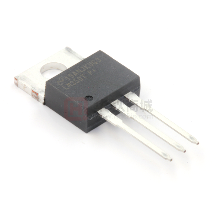
Connection Diagram
Case is Output
Figure 1. (TO-3 STEEL) Metal Can Package
Bottom View
See Package Number NDS0002A
Figure 2. (TO-220) Plastic Package
Front View
See Package Number NDE0003B
1
2
Please be aware that an important notice concerning availability, standard warranty, and use in critical applications of
Texas Instruments semiconductor products and disclaimers thereto appears at the end of this data sheet.
All trademarks are the property of their respective owners.
PRODUCTION DATA information is current as of publication date.
Products conform to specifications per the terms of the Texas
Instruments standard warranty. Production processing does not
necessarily include testing of all parameters.
Copyright © 1998–2013, Texas Instruments Incorporated
�LM150, LM350-N, LM350A
SNVS772B – MAY 1998 – REVISED MARCH 2013
www.ti.com
These devices have limited built-in ESD protection. The leads should be shorted together or the device placed in conductive foam
during storage or handling to prevent electrostatic damage to the MOS gates.
Absolute Maximum Ratings (1) (2) (3)
Power Dissipation
Internally Limited
Input-Output Voltage Differential
+35V
−65°C to +150°C
Storage Temperature
Lead Temperature
Metal Package (Soldering, 10 sec.)
300°C
Plastic Package (Soldering, 4 sec.)
260°C
ESD Tolerance
TBD
Operating Temperature Range
LM150
−55°C ≤ TJ ≤ +150°C
LM350A
−40°C ≤ TJ ≤ +125°C
0°C ≤ TJ ≤ +125°C
LM350
(1)
(2)
(3)
Absolute Maximum Ratings indicate limits beyond which damage to the device may occur. Operating Ratings indicate conditions for
which the device is intended to be functional, but do not ensure specific performance limits. For ensured specifications and test
conditions, see the Electrical Characteristics.
Refer to RETS150K drawing for military specifications of the LM150K.
If Military/Aerospace specified devices are required, please contact the Texas Instruments Sales Office/ Distributors for availability and
specifications.
Electrical Characteristics
Specifications with standard type face are for TJ= 25°C, and those with boldface type apply over full Operating
Temperature Range. Unless otherwise specified, VIN− VOUT= 5V, and IOUT= 10 mA (1)
Parameter
Conditions
LM150
Min
Reference Voltage
3V ≤ (VIN − VOUT) ≤ 35V, 10 mA ≤ IOUT ≤ 3A, P ≤ 30W
Line Regulation
3V ≤ (VIN − VOUT) ≤ 35V (2)
Load Regulation
10 mA ≤ IOUT ≤ 3A (2)
Thermal Regulation
20 ms Pulse
1.20
Adjustment Pin Current
Typ
Max
1.25
1.30
V
0.005
0.01
%/V
0.02
0.05
%/V
0.1
0.3
%
0.3
1
%
0.002
0.01
%/W
50
100
μA
0.2
5
μA
5
mA
Adjustment Pin Current Change
10 mA ≤ IOUT ≤ 3A, 3V ≤ (VIN − VOUT) ≤ 35V
Temperature Stability
TMIN ≤ TJ ≤ TMAX
1
Minimum Load Current
VIN − VOUT = 35V
3.5
Current Limit
RMS Output Noise, % of VOUT
Ripple Rejection Ratio
Units
%
VIN − VOUT ≤ 10V
3.0
4.5
VIN − VOUT = 30V
0.3
1
A
0.001
%
65
dB
10 Hz ≤ f ≤ 10 kHz
VOUT = 10V, f = 120 Hz, CADJ = 0 μF
VOUT = 10V, f = 120 Hz, CADJ = 10 μF
66
A
86
dB
Long-Term Stability
TJ = 125°C, 1000 hrs
0.3
1
%
Thermal Resistance, Junction to Case
NDS Package
1.2
1.5
°C/W
Thermal Resistance, Junction to
Ambient (No Heat Sink)
NDS Package
35
(1)
(2)
2
°C/W
These specifications are applicable for power dissipations up to 30W for the TO-3 (NDS) package and 25W for the TO-220 (NDE)
package. Power dissipation is ensured at these values up to 15V input-output differential. Above 15V differential, power dissipation will
be limited by internal protection circuitry. All limits (i.e., the numbers in the Min. and Max. columns) are ensured to AOQL (Average
Outgoing Quality Level).
Regulation is measured at a constant junction temperature, using pulse testing with a low duty cycle. Changes in output voltage due to
heating effects are covered under the specifications for thermal regulation.
Submit Documentation Feedback
Copyright © 1998–2013, Texas Instruments Incorporated
Product Folder Links: LM150 LM350-N LM350A
�LM150, LM350-N, LM350A
www.ti.com
SNVS772B – MAY 1998 – REVISED MARCH 2013
Electrical Characteristics
Specifications with standard type face are for TJ = 25°C, and those with boldface type apply over full Operating
Temperature Range. Unless otherwise specified, VIN − VOUT = 5V, and IOUT = 10 mA. (1)
Parameter
Conditions
Reference Voltage
IOUT = 10 mA, TJ = 25°C
3V ≤ (VIN − VOUT) ≤ 35V,
10 mA ≤ IOUT ≤ 3A, P ≤ 30W
Line Regulation
3V ≤ (VIN − VOUT) ≤ 35V (2)
Load Regulation
10 mA ≤ IOUT ≤ 3A (2)
Thermal Regulation
20 ms Pulse
LM350A
Typ
Max
1.238
1.250
1.262
1.225
1.250
1.270
0.005
Adjustment Pin Current
Adjustment Pin Current Change
10 mA ≤ IOUT ≤ 3A, 3V ≤ (VIN − VOUT) ≤ 35V
Temperature Stability
TMIN ≤ TJ ≤ TMAX
Minimum Load Current
VIN − VOUT = 35V
Current Limit
RMS Output Noise, % of VOUT
Ripple Rejection Ratio
Long-Term Stability
Typ
Max
1.20
1.25
1.30
V
0.01
0.005
0.03
%/V
0.02
0.05
0.02
0.07
%/V
0.1
0.3
0.1
0.5
%
0.3
1
0.3
1.5
%
0.002
0.01
0.002
0.03
%/W
50
100
50
100
μA
0.2
5
0.2
5
μA
V
1
3.5
1
10
3.5
%
10
mA
VIN − VOUT ≤ 10V
3.0
4.5
3.0
4.5
A
VIN − VOUT = 30V
0.3
1
0.25
1
A
10 Hz ≤ f ≤ 10 kHz
VOUT = 10V, f = 120 Hz, CADJ = 0 μF
VOUT = 10V, f = 120 Hz, CADJ = 10 μF
TJ = 125°C, 1000 hrs
Thermal Resistance, Junction to NDS Package
Ambient (No Heat Sink)
NDE Package
(2)
Units
Min
66
0.001
0.001
%
65
65
dB
86
dB
86
0.25
Thermal Resistance, Junction to NDS Package
Case
NDE Package
(1)
LM350
Min
3
50
66
1
4
0.25
1
%
1.2
1.5
°C/W
3
4
°C/W
35
°C/W
50
°C/W
These specifications are applicable for power dissipations up to 30W for the TO-3 (NDS) package and 25W for the TO-220 (NDE)
package. Power dissipation is ensured at these values up to 15V input-output differential. Above 15V differential, power dissipation will
be limited by internal protection circuitry. All limits (i.e., the numbers in the Min. and Max. columns) are ensured to AOQL (Average
Outgoing Quality Level).
Regulation is measured at a constant junction temperature, using pulse testing with a low duty cycle. Changes in output voltage due to
heating effects are covered under the specifications for thermal regulation.
Copyright © 1998–2013, Texas Instruments Incorporated
Product Folder Links: LM150 LM350-N LM350A
Submit Documentation Feedback
3
�LM150, LM350-N, LM350A
SNVS772B – MAY 1998 – REVISED MARCH 2013
www.ti.com
Typical Performance Characteristics
4
Load Regulation
Current Limit
Figure 3.
Figure 4.
Adjustment Current
Dropout Voltage
Figure 5.
Figure 6.
Temperature Stability
Minimum Operating Current
Figure 7.
Figure 8.
Submit Documentation Feedback
Copyright © 1998–2013, Texas Instruments Incorporated
Product Folder Links: LM150 LM350-N LM350A
�LM150, LM350-N, LM350A
www.ti.com
SNVS772B – MAY 1998 – REVISED MARCH 2013
Typical Performance Characteristics (continued)
Ripple Rejection
Ripple Rejection
Figure 9.
Figure 10.
Ripple Rejection
Output Impedance
Figure 11.
Figure 12.
Line Transient Response
Load Transient Response
Figure 13.
Figure 14.
Copyright © 1998–2013, Texas Instruments Incorporated
Product Folder Links: LM150 LM350-N LM350A
Submit Documentation Feedback
5
�LM150, LM350-N, LM350A
SNVS772B – MAY 1998 – REVISED MARCH 2013
www.ti.com
APPLICATION HINTS
In operation, the LM150 develops a nominal 1.25V reference voltage, VREF, between the output and adjustment
terminal. The reference voltage is impressed across program resistor R1 and, since the voltage is constant, a
constant current I1 then flows through the output set resistor R2, giving an output voltage of
(1)
Figure 15.
Since the 50 μA current from the adjustment terminal represents an error term, the LM150 was designed to
minimize IADJ and make it very constant with line and load changes. To do this, all quiescent operating current is
returned to the output establishing a minimum load current requirement. If there is insufficient load on the output,
the output will rise.
EXTERNAL CAPACITORS
An input bypass capacitor is recommended. A 0.1 μF disc or 1 μF solid tantalum on the input is suitable input
bypassing for almost all applications. The device is more sensitive to the absence of input bypassing when
adjustment or output capacitors are used but the above values will eliminate the possibility of problems.
The adjustment terminal can be bypassed to ground on the LM150 to improve ripple rejection. This bypass
capacitor prevents ripple from being amplified as the output voltage is increased. With a 10 μF bypass capacitor
86 dB ripple rejection is obtainable at any output level. Increases over 10 μF do not appreciably improve the
ripple rejection at frequencies above 120 Hz. If the bypass capacitor is used, it is sometimes necessary to
include protection diodes to prevent the capacitor from discharging through internal low current paths and
damaging the device.
In general, the best type of capacitors to use is solid tantalum. Solid tantalum capacitors have low impedance
even at high frequencies. Depending upon capacitor construction, it takes about 25 μF in aluminum electrolytic to
equal 1 μF solid tantalum at high frequencies. Ceramic capacitors are also good at high frequencies, but some
types have a large decrease in capacitance at frequencies around 0.5 MHz. For this reason, 0.01 μF disc may
seem to work better than a 0.1 μF disc as a bypass.
Although the LM150 is stable with no output capacitors, like any feedback circuit, certain values of external
capacitance can cause excessive ringing. This occurs with values between 500 pF and 5000 pF. A 1 μF solid
tantalum (or 25 μF aluminum electrolytic) on the output swamps this effect and insures stability.
LOAD REGULATION
The LM150 is capable of providing extremely good load regulation but a few precautions are needed to obtain
maximum performance. The current set resistor connected between the adjustment terminal and the output
terminal (usually 240Ω) should be tied directly to the output (case) of the regulator rather than near the load. This
eliminates line drops from appearing effectively in series with the reference and degrading regulation. For
example, a 15V regulator with 0.05Ω resistance between the regulator and load will have a load regulation due to
line resistance of 0.05Ω × IOUT. If the set resistor is connected near the load the effective line resistance will be
0.05Ω (1 + R2/R1) or in this case, 11.5 times worse.
Figure 16 shows the effect of resistance between the regulator and 240Ω set resistor.
6
Submit Documentation Feedback
Copyright © 1998–2013, Texas Instruments Incorporated
Product Folder Links: LM150 LM350-N LM350A
�LM150, LM350-N, LM350A
www.ti.com
SNVS772B – MAY 1998 – REVISED MARCH 2013
Figure 16. Regulator with Line Resistance
in Output Lead
With the TO-3 package, it is easy to minimize the resistance from the case to the set resistor, by using two
separate leads to the case. The ground of R2 can be returned near the ground of the load to provide remote
ground sensing and improve load regulation.
PROTECTION DIODES
When external capacitors are used with any IC regulator it is sometimes necessary to add protection diodes to
prevent the capacitors from discharging through low current points into the regulator. Most 10 μF capacitors have
low enough internal series resistance to deliver 20A spikes when shorted. Although the surge is short, there is
enough energy to damage parts of the IC.
When an output capacitor is connected to a regulator and the input is shorted, the output capacitor will discharge
into the output of the regulator. The discharge current depends on the value of the capacitor, the output voltage
of the regulator, and the rate of decrease of VIN. In the LM150, this discharge path is through a large junction that
is able to sustain 25A surge with no problem. This is not true of other types of positive regulators. For output
capacitors of 25 μF or less, there is no need to use diodes.
The bypass capacitor on the adjustment terminal can discharge through a low current junction. Discharge occurs
when either the input or output is shorted. Internal to the LM150 is a 50Ω resistor which limits the peak discharge
current. No protection is needed for output voltages of 25V or less and 10 μF capacitance. Figure 17 shows an
LM150 with protection diodes included for use with outputs greater than 25V and high values of output
capacitance.
D1 protects against C1
D2 protects against C2
Figure 17. Regulator with Protection Diodes
(2)
Copyright © 1998–2013, Texas Instruments Incorporated
Product Folder Links: LM150 LM350-N LM350A
Submit Documentation Feedback
7
�LM150, LM350-N, LM350A
SNVS772B – MAY 1998 – REVISED MARCH 2013
www.ti.com
Schematic Diagram
Figure 18. Schematic Diagram
Typical Applications
Full output current not available
at high input-output voltages.
†Optional—improves transient response. Output capacitors in the range of 1 μF to 1000 μF of aluminum or tantalum
electrolytic are commonly used to provide improved output impedance and rejection of transients.
*Needed if device is more than 6 inches from filter capacitors.
Figure 19. 1.2V–25V Adjustable Regulator
Note: Usually R1 = 240Ω for LM150 and R1 = 120Ω for LM350.
(3)
8
Submit Documentation Feedback
Copyright © 1998–2013, Texas Instruments Incorporated
Product Folder Links: LM150 LM350-N LM350A
�LM150, LM350-N, LM350A
www.ti.com
SNVS772B – MAY 1998 – REVISED MARCH 2013
*Adjust for 3.75V across R1
Figure 20. Precision Power Regulator with Low Temperature Coefficient
Figure 21. Slow Turn-ON 15V Regulator
†Solid tantalum
*Discharges C1 if output is shorted to ground
Figure 22. Adjustable Regulator with Improved Ripple Rejection
Copyright © 1998–2013, Texas Instruments Incorporated
Product Folder Links: LM150 LM350-N LM350A
Submit Documentation Feedback
9
�LM150, LM350-N, LM350A
SNVS772B – MAY 1998 – REVISED MARCH 2013
www.ti.com
Figure 23. High Stability 10V Regulator
*Sets maximum VOUT
Figure 24. Digitally Selected Outputs
Figure 25. Regulator and Voltage Reference
10
Submit Documentation Feedback
Copyright © 1998–2013, Texas Instruments Incorporated
Product Folder Links: LM150 LM350-N LM350A
�LM150, LM350-N, LM350A
www.ti.com
SNVS772B – MAY 1998 – REVISED MARCH 2013
*Minimum load current 50 mA
Figure 26. 10A Regulator
*Min output ≈ 1.2V
Figure 27. 5V Logic Regulator with Electronic Shutdown*
Full output current not available at high input-output voltages
Figure 28. 0 to 30V Regulator
Copyright © 1998–2013, Texas Instruments Incorporated
Product Folder Links: LM150 LM350-N LM350A
Submit Documentation Feedback
11
�LM150, LM350-N, LM350A
SNVS772B – MAY 1998 – REVISED MARCH 2013
www.ti.com
†Solid tantalum
*Lights in constant current mode
Figure 29. 5A Constant Voltage/Constant Current Regulator
Figure 30. 12V Battery Charger
*0.4 ≤ R1 ≤ 120Ω
12
Submit Documentation Feedback
Copyright © 1998–2013, Texas Instruments Incorporated
Product Folder Links: LM150 LM350-N LM350A
�LM150, LM350-N, LM350A
www.ti.com
SNVS772B – MAY 1998 – REVISED MARCH 2013
Figure 31. Adjustable Current Regulator
Figure 32. Precision Current Limiter
*Minimum output current ≈ 4 mA
Figure 33. 1.2V–20V Regulator with Minimum
Program Current
Figure 34. 3A Current Regulator
Figure 35. Tracking Preregulator
†Minimum load—10 mA
*All outputs within ±100 mV
Figure 36. Adjusting Multiple On-Card Regulators with Single Control*
Copyright © 1998–2013, Texas Instruments Incorporated
Product Folder Links: LM150 LM350-N LM350A
Submit Documentation Feedback
13
�LM150, LM350-N, LM350A
SNVS772B – MAY 1998 – REVISED MARCH 2013
www.ti.com
Use of RS allows low charging rates with fully charged battery.
**1000 μF is recommended to filter out any input transients
Figure 37. AC Voltage Regulator
Figure 38. Simple 12V Battery Charger
Figure 39. Temperature Controller
Figure 40. Light Controller
*Sets peak current (2A for 0.3Ω)
**1000 μF is recommended to filter out any input transients.
14
Submit Documentation Feedback
Copyright © 1998–2013, Texas Instruments Incorporated
Product Folder Links: LM150 LM350-N LM350A
�LM150, LM350-N, LM350A
www.ti.com
SNVS772B – MAY 1998 – REVISED MARCH 2013
Figure 41. Adjustable 10A Regulator
Figure 42. Current Limited 6V Charger
Figure 43. 6A Regulator
Copyright © 1998–2013, Texas Instruments Incorporated
Product Folder Links: LM150 LM350-N LM350A
Submit Documentation Feedback
15
�LM150, LM350-N, LM350A
SNVS772B – MAY 1998 – REVISED MARCH 2013
www.ti.com
REVISION HISTORY
Changes from Revision A (March 2013) to Revision B
•
16
Page
Changed layout of National Data Sheet to TI format .......................................................................................................... 15
Submit Documentation Feedback
Copyright © 1998–2013, Texas Instruments Incorporated
Product Folder Links: LM150 LM350-N LM350A
�PACKAGE OPTION ADDENDUM
www.ti.com
30-Sep-2021
PACKAGING INFORMATION
Orderable Device
Status
(1)
Package Type Package Pins Package
Drawing
Qty
Eco Plan
(2)
Lead finish/
Ball material
MSL Peak Temp
Op Temp (°C)
Device Marking
(3)
(4/5)
(6)
LM350A MWC
ACTIVE
WAFERSALE
YS
0
1
RoHS & Green
Call TI
Level-1-NA-UNLIM
-40 to 85
LM350AT
NRND
TO-220
NDE
3
45
Non-RoHS
& Green
Call TI
Level-1-NA-UNLIM
-40 to 125
LM350AT
P+
LM350AT/NOPB
ACTIVE
TO-220
NDE
3
45
RoHS & Green
SN
Level-1-NA-UNLIM
-40 to 125
LM350AT
P+
LM350K STEEL
ACTIVE
TO-3
NDS
2
50
Non-RoHS &
Non-Green
Call TI
Call TI
0 to 125
LM350K
STEELP+
LM350K STEEL/NOPB
ACTIVE
TO-3
NDS
2
50
RoHS & Green
Call TI
Level-1-NA-UNLIM
0 to 125
LM350K
STEELP+
LM350T
NRND
TO-220
NDE
3
45
Non-RoHS
& Green
Call TI
Level-1-NA-UNLIM
0 to 125
LM350T P+
LM350T/NOPB
ACTIVE
TO-220
NDE
3
45
RoHS & Green
SN
Level-1-NA-UNLIM
0 to 125
LM350T P+
(1)
The marketing status values are defined as follows:
ACTIVE: Product device recommended for new designs.
LIFEBUY: TI has announced that the device will be discontinued, and a lifetime-buy period is in effect.
NRND: Not recommended for new designs. Device is in production to support existing customers, but TI does not recommend using this part in a new design.
PREVIEW: Device has been announced but is not in production. Samples may or may not be available.
OBSOLETE: TI has discontinued the production of the device.
(2)
RoHS: TI defines "RoHS" to mean semiconductor products that are compliant with the current EU RoHS requirements for all 10 RoHS substances, including the requirement that RoHS substance
do not exceed 0.1% by weight in homogeneous materials. Where designed to be soldered at high temperatures, "RoHS" products are suitable for use in specified lead-free processes. TI may
reference these types of products as "Pb-Free".
RoHS Exempt: TI defines "RoHS Exempt" to mean products that contain lead but are compliant with EU RoHS pursuant to a specific EU RoHS exemption.
Green: TI defines "Green" to mean the content of Chlorine (Cl) and Bromine (Br) based flame retardants meet JS709B low halogen requirements of


 工商网监
湘ICP备2023018690号
工商网监
湘ICP备2023018690号
