LM3639A
www.ti.com
SNVS964 – MARCH 2013
LM3639A Single Chip 40V Backlight + 1.5A Flash LED Driver
Check for Samples: LM3639A
FEATURES
DESCRIPTION
•
The LM3639A is a single-chip white LED Camera
Flash Driver + LCD Display Backlight Driver. The lowvoltage, high-current flash LED driver is a
synchronous boost which provides the power for a
single flash LED at up to 1.5A or dual LEDs at up to
750 mA each. The high-voltage backlight driver is a
dual-output asynchronous boost which powers dual
LED strings at up to 40V and 30 mA per string. An
adaptive regulation method in both boost converters
regulates the headroom voltage across the respective
source/sink to ensure the LED current remains in
regulation
while
maximizing
efficiency.
The
LM3639A's flash driver is a 2MHz or 4MHz fixedfrequency synchronous boost converter plus 1.5A
constant current driver for a high-current white LED.
The high-side current source allows for grounded
cathode LED operation providing Flash current up to
1.5A. An adaptive regulation method ensures the
current source remains in regulation and maximizes
efficiency.
1
2
•
•
•
•
•
•
•
•
Single Chip White LED Flash and Backlight
Driver
1.5A Flash LED Current
Dual String Backlight Control (40V Max VOUT)
128 Level Exponential and Linear Brightness
Control
PWM Input for CABC
Programmable Over-Voltage Protection
(Backlight)
Programmable Current Limit (Flash)
Programmable Switching Frequency
Optimized Flash Current During Low-Battery
Conditions
APPLICATIONS
•
•
White LED Backlit Display Power
White LED Camera Flash Power
L(B)
Schottky
L(F)
COUTB
SWF SWB
VIN
2.5V - 5.5V
VOUTB
up to 40V
OVP
OUTF
CIN
OR
EN
SCL
SDA
LM3639A
COUTF
STROBE
BLED1
BLED2
TX
FLED1
FLED2
PWM
FLED2
GND
FLED1
The device is controlled by an I2C-compatible
interface. Features for the flash LED driver include a
hardware flash enable (STROBE) allowing a logic
input to trigger the flash pulse, and a TX input for
synchronization to RF power amplifier events or other
high current conditions. Features for the LCD
backlight driver include a PWM input for content
adjustable backlight control, 128 exponential or linear
brightness
levels,
programmable
over-voltage
protection, and selectable switching frequency (500
kHz or 1 MHz).
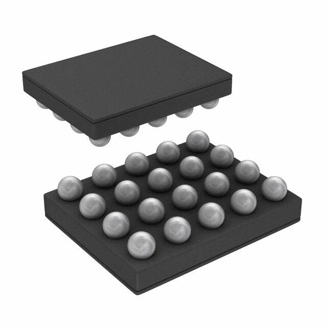
The device is available in a tiny 1.790 mm x 2.165
mm x 0.6 mm 20-bump, 0.4 mm pitch DSBGA
package and operates over the −40°C to +85°C
temperature range.
1
2
Please be aware that an important notice concerning availability, standard warranty, and use in critical applications of
Texas Instruments semiconductor products and disclaimers thereto appears at the end of this data sheet.
All trademarks are the property of their respective owners.
PRODUCTION DATA information is current as of publication date.
Products conform to specifications per the terms of the Texas
Instruments standard warranty. Production processing does not
necessarily include testing of all parameters.
Copyright © 2013, Texas Instruments Incorporated
�LM3639A
SNVS964 – MARCH 2013
www.ti.com
This integrated circuit can be damaged by ESD. Texas Instruments recommends that all integrated circuits be handled with
appropriate precautions. Failure to observe proper handling and installation procedures can cause damage.
ESD damage can range from subtle performance degradation to complete device failure. Precision integrated circuits may be more
susceptible to damage because very small parametric changes could cause the device not to meet its published specifications.
Connection Diagram
4
4
3
3
2
2
1
1
A
B
C
D
E
E
Top View
D
C
B
A
Bottom View
Figure 1. 20-Bump, 0.4 mm Pitch DSBGA Package
YFQ0020HGA
PIN DESCRIPTIONS
TERMINAL
NAME
NO.
I/O
DESCRIPTION
FLED1
A1
Output
High Side Current Source Output for Flash LED1.
FLED2
B1
Output
High Side Current Source Output for Flash LED2.
OUTF (x2)
A2/B2
Output
Flash LED Boost Output. Connect a 10 µF ceramic capacitor between this
pin GND.
SWF (x2)
A3/B3
Output
Drain Connection for Internal NMOS and Synchronous PMOS Switches.
Connect the Flash LED Boost Inductor to SWF.
GND (x3)
A4/B4/E3
Ground
TX
C2
Input
Power Amplifier Synchronization Input. The TX pin has a 300 kΩ pull-down
resistor connected to GND.
STROBE
C3
Input
Active High Hardware Flash Enable. Drive STROBE high to turn on Flash
pulse. STROBE overrides TORCH. The STROBE pin has a 300 kΩ pulldown resistor connected to GND.
VIN
C4
Input
Input Voltage Connection. Connect IN to the input supply, and bypass to
GND with a 10 µF or larger ceramic capacitor.
SDA
D3
Input
Serial Data Input/Output.
SCL
D2
Input
Serial Clock Input.
EN
C1
Input
Enable Pin. High = Standby, Low = Shutdown/Reset.
SWB
E4
Input
Drain Connection for internal NFET. Connect SWB to the junction of the
backlight boost inductor and the Schottky diode anode.
PWM
D4
Input
PWM Brightness Control Input for backlight current control. The PWM pin
has a 300 kΩ pull-down resistor connected to GND.
BLED1
D1
Input
Input Terminal to Backlight LED String Current Sink #1 (40V max). The boost
converter regulates the minimum of BLED1 and BLED2 to 400 mV.
BLED2
E1
Input
Input Terminal to Backlight LED String Current Sink #2 (40V max). The boost
converter regulates the minimum of BLED1 and BLED2 to 400 mV.
OVP
E2
Input
Over-Voltage Sense Input for Backlight Boost. Connect to the positive
terminal of (COUTB).
2
Submit Documentation Feedback
Copyright © 2013, Texas Instruments Incorporated
Product Folder Links: LM3639A
�LM3639A
www.ti.com
SNVS964 – MARCH 2013
ABSOLUTE MAXIMUM RATINGS
VIN
(1)
(2) (3)
−0.3V to 6V
SWF, OUTF, FLED1, FLED2, EN, PWM, SCL, SDA, TX, STROBE
SWB, OVP, BLED1, BLED2
(2)
(2)
−0.3V to +45V
−65°C to +150°C
Storage Temperature Range
(1)
(2)
(3)
Absolute Maximum Ratings indicate limits beyond which damage to the device may occur. Operating Ratings are conditions under
which operation of the device is ensured. Operating Ratings do not imply ensured performance limits. For ensured performance limits
and associated test conditions, see the Electrical Characteristics table.
All voltages are with respect to the potential at the GND pin.
VIN can be below −0.3V if the current out of the pin is limited to 500 µA.
OPERATING RATINGS
(1) (2)
VIN
2.5V to 5.5V
−40°C to +125°C
Junction Temperature (TJ)
Ambient Temperature (TA)
(1)
(2)
(3)
−0.3V to the lesser of (VIN+0.3V) w/ 6V
max
(3)
−40°C to +85°C
Absolute Maximum Ratings indicate limits beyond which damage to the device may occur. Operating Ratings are conditions under
which operation of the device is ensured. Operating Ratings do not imply ensured performance limits. For ensured performance limits
and associated test conditions, see the Electrical Characteristics table.
All voltages are with respect to the potential at the GND pin.
In applications where high power dissipation and/or poor package thermal resistance is present, the maximum ambient temperature may
have to be derated. Maximum ambient temperature (TA-MAX) is dependent on the maximum operating junction temperature (TJ-MAX-OP =
+125°C), the maximum power dissipation of the device in the application (PD-MAX), and the junction-to-ambient thermal resistance of the
part/package in the application (θJA), as given by the following equation: TA-MAX = TJ-MAX-OP – (θJA × PD-MAX).
THERMAL PROPERTIES
Thermal Junction-to-Ambient Resistance (θJA)
(1)
(1)
48.8°C/W
Junction-to-ambient thermal resistance (θJA) is taken from a thermal modeling result, performed under the conditions and guidelines set
forth in the JEDEC standard JESD51-7. The test board is a 4-layer FR-4 board measuring 102mm x 76mm x 1.6mm with a 2 x 1 array
of thermal vias. The ground plane on the board is 50mm x 50mm. Thickness of copper layers are 36μm/18μm/18μm/36μm
(1.5oz/1oz/1oz/1.5oz). Ambient temperature in simulation is 22°C in still air. Power dissipation is 1W. In applications where high
maximum power dissipation exists special care must be paid to thermal dissipation issues.
Submit Documentation Feedback
Copyright © 2013, Texas Instruments Incorporated
Product Folder Links: LM3639A
3
�LM3639A
SNVS964 – MARCH 2013
www.ti.com
ELECTRICAL CHARACTERISTICS
(1) (2)
Limits in standard typeface are for TA = +25°C. Limits in boldface type apply over the full operating ambient temperature
range (−40°C ≤ TA ≤ +85°C). Unless otherwise specified, VIN = 3.6V.
Symbol
Parameter
VIN
Input Voltage Range
ISHDN
Shutdown Supply Current
Standby Supply Current
ISB
Test Conditions
Min
Typ
Max
Unit
2.5
3.6
5.5
V
Device Shutdown, EN = GND
1
3.5
Device Disabled via I2C
EN = VIN
1
4
µA
Low Voltage Boost Specifications (Flash Driver)
IFLED1 + IFLED2
Current Source Accuracy
2.7V ≤ VIN ≤ 5.5V
750 mA Flash
Current Setting
−7%
1.5
+7%
A
28.125 mA Torch
Current Setting,
per current
source
−10%
56.25
+10%
mA
For 750 mA Flash Current Setting
315
For 28.125 mA Torch Current Setting
180
VHR1, VHR2
Regulated Headroom Voltage
VOVP
Output Over-Voltage
Protection Trip Point
ON Threshold
4.87
5
5.10
OFF Threshold
4.71
4.88
4.98
RPMOS
PMOS Switch On-Resistance
IPMOS = 1A
85
RNMOS
NMOS Switch On-Resistance
INMOS = 1A
75
VIN = 3.6V
mV
V
mΩ
−12%
1.7
12%
−12%
1.9
12%
−12%
2.5
12%
−12%
3.1
12%
ICL
Switch Current Limit
VIVM
Input Voltage Monitor
Threshold
VIN Falling
−4%
2.5
4%
V
fSW
Switching Frequency
2.5V ≤ VIN ≤ 5.5V
3.64
4.00
4.36
MHz
IQ
Quiescent Supply Current
Device Not Switching
Pass Mode, Backlight Disabled
0.6
2
mA
tTX
Flash to Torch LED Current
Settling Time
TX low to High, ILED1,2 = 750 mA to
23.44 mA
4
A
µs
High Voltage Boost Specification (Backlight Driver)
IBLED1, IBLED2
Output Current Regulation
(BLED1 or BLED2)
2.7V ≤ VIN ≤ 5.5V, Full Scale Current =
19 mA, Brightness Register = 0xFF
IMATCH_HV
BLED1 to BLED2 Current
Matching (3)
2.7V ≤ VIN ≤ 5.5V, Full Scale Current =
19 mA, Brightness Register = 0xFF
VREG_CS
Regulated Current Sink
Headroom Voltage
ILED = 19mA
400
VHR_MIN
Current Sink Minimum
Headroom Voltage
ILED = 95% of ILED = 19 mA
130
RDSON
NMOS Switch On Resistance
ISW = 500 mA
ICL_BOOST
NMOS Switch Current Limit
VIN = 3.6V
VOVP
Output Over-Voltage
Protection
fSW
Switching Frequency
DMAX
Maximum Duty Cycle
(1)
(2)
(3)
4
−7%
19
7%
mA
1
2.25
%
mV
ON Threshold, 2.7V ≤ VIN ≤ 5.5V,
OVP select bits = 11
230
1
10%
38.4
40.0
41.4
Hysteresis
2.5V ≤ VIN ≤ 5.5V,
Boost Frequency
Select Bit = '0'
mΩ
−10%
A
V
1
465
500
94
535
kHz
%
All voltages are with respect to the potential at the GND pin.
JESD ESD tests are applied at the ASIC level. The human body model is a 100 pF capacitor discharged through a 1.5 kΩ resistor into
each pin. The machine model is a 200 pF capacitor discharged directly into each pin.
Matching (%)= 100 × (|(ILED1 - ILED2 )| / (ILED1 + ILED2))
Submit Documentation Feedback
Copyright © 2013, Texas Instruments Incorporated
Product Folder Links: LM3639A
�LM3639A
www.ti.com
SNVS964 – MARCH 2013
ELECTRICAL CHARACTERISTICS (1) (2) (continued)
Limits in standard typeface are for TA = +25°C. Limits in boldface type apply over the full operating ambient temperature
range (−40°C ≤ TA ≤ +85°C). Unless otherwise specified, VIN = 3.6V.
Symbol
Parameter
Test Conditions
Min
Typ
Max
Unit
Logic Input Voltage Specifications (EN, STROBE, TORCH, TX, PWM)
VIL
Input Logic Low
2.5V ≤ VIN ≤ 5.5V
0
0.4
VIH
Input Logic High
2.5V ≤ VIN ≤ 5.5V
1.2
VIN
V
Logic Input Voltage Specifications (SCL, SDA)
VOL
Output Logic Low (SDA only)
ILOAD = 3 mA
400
VIL
Input Logic Low
2.5V ≤ VIN ≤ 5.5V
0
0.4
VIH
Input Logic High
2.5V ≤ VIN ≤ 4.2V
1.2
VIN
mV
V
I2C-Compatible Timing Specifications (SCL, SDA)
1/t1
SCL (Clock Frequency)
t2
Data In Setup Time to SCL
High
kHz
100
t3
Data Out Stable After SCL
Low
0
t4
SDA Low Setup Time to SCL
Low (Start)
100
t5
SDA High Hold Time After
SCL High (Stop)
100
ns
SDA
SDA
Figure 2. I2C Timing Diagram
Submit Documentation Feedback
Copyright © 2013, Texas Instruments Incorporated
Product Folder Links: LM3639A
5
�LM3639A
SNVS964 – MARCH 2013
www.ti.com
TYPICAL PERFORMANCE CHARACTERISTICS
Unless otherwise specified: TA = 25°C; VIN = 3.6V; VEN = VIN; CIN= 10 μF, COUTF= 10 μF, COUTB = 1 μF (50V 0805 case
size); LF = 1 μH; LB = 22 μH.
0.8
0.78
0.77
0.78
0.77
0.76
0.75
0.74
0.73
0.76
0.75
0.74
0.73
0.72
0.72
fSW = 2MHz
0.71
fSW = 4MHz
0.71
0.7
0.7
2.7
3
3.3
3.6
3.9
4.2
4.5
4.8
VIN (V)
2.7
3
3.3
3.6
3.9
4.2
4.5
C004
Figure 4. Flash LED Current Line Regulation @ fSW = 4MHz
0.8
2
0.7
1.9
0.6
1.8
ICL = 1.7A
1.7
0.5
IIN (A)
0.4
0.3
D1,+25°C
D2,+25°C
D1,-40°C
D2,-40°C
D1,+85°C
D2,+85°C
0.2
0.1
0
1
2
3
4
5
6
7
8
9
10
11
12
13
1.6
1.5
1.4
0
14
15
Flash Code (#)
1.3
2MHz,+25 C
1.2
2MHz,-40 C
1.1
2MHz,+85 C
1
C006
2.5
3
3.5
4
4.5
5
VIN (V)
Figure 5. Flash LED Current vs Brightness Code
C008
2
ICL = 1.7A
ICL = 1.9A
1.9
1.8
1.8
1.7
1.7
1.6
1.6
IIN (A)
IIN (A)
5.5
Figure 6. Input Current vs Input Voltage, IFLASH = 1.5A
2
1.9
1.5
1.4
1.5
1.4
1.3
4MHz,+25 C
1.3
2MHz,+25 C
1.2
4MHz,-40 C
1.2
2MHz,-40 C
4MHz,+85 C
1.1
2MHz,+85 C
1.1
1
1
2.5
3
3.5
4
VIN (V)
4.5
5
5.5
2.5
3
3.5
4
VIN (V)
C008
Figure 7. Input Current vs Input Voltage, IFLASH = 1.5A
6
4.8
VIN (V)
C004
Figure 3. Flash LED Current Line Regulation @ fSW = 2MHz
ILED (A)
D1, +25°C
D2, +25°C
D1, +85°C
D2, +85°C
D1, -40°C
D2, -40°C
0.79
ILED (A)
ILED (A)
0.8
D1, +25°C
D2, +25°C
D1, +85°C
D2, +85°C
D1, -40°C
D2, -40°C
0.79
4.5
5
5.5
C008
Figure 8. Input Current vs Input Voltage, IFLASH = 1.5A
Submit Documentation Feedback
Copyright © 2013, Texas Instruments Incorporated
Product Folder Links: LM3639A
�LM3639A
www.ti.com
SNVS964 – MARCH 2013
TYPICAL PERFORMANCE CHARACTERISTICS (continued)
Unless otherwise specified: TA = 25°C; VIN = 3.6V; VEN = VIN; CIN= 10 μF, COUTF= 10 μF, COUTB = 1 μF (50V 0805 case
size); LF = 1 μH; LB = 22 μH.
2
3
ICL = 1.9A
1.8
2.6
2MHz,-40 C
1.7
2.4
2MHz,+85 C
1.6
2.2
1.5
1.4
2
1.3
4MHz,+25 C
1.6
1.2
4MHz,-40 C
1.4
1.1
4MHz,+85 C
1.2
1
2.5
3
3.5
4
4.5
5
VIN (V)
5.5
2.5
3
3.5
4
4.5
5
VIN (V)
C008
Figure 9. Input Current vs Input Voltage, IFLASH = 1.5A
5.5
C008
Figure 10. Input Current vs Input Voltage, IFLASH = 1.5A
3
3
ICL = 2.5A
2.8
4MHz,+25 C
2.6
4MHz,-40 C
2.6
2.4
4MHz,+85 C
2.4
ICL = 3.1A
2.8
2.2
IIN (A)
IIN (A)
ICL = 2.5A
1.8
1
2
2MHz,+25 C
2.2
2MHz,-40 C
2
1.8
1.8
1.6
1.6
1.4
1.4
1.2
1.2
1
2MHz,+85 C
1
2.5
3
3.5
4
4.5
5
VIN (V)
5.5
2.5
3
3.5
4
4.5
5
VIN (V)
C008
Figure 11. Input Current vs Input Voltage, IFLASH = 1.5A
5.5
C008
Figure 12. Input Current vs Input Voltage, IFLASH = 1.5A
3
100%
ICL = 3.1A
2.8
fSW = 2MHz
2.6
90%
2.4
4MHz,+25 C
(%)
2.2
4MHz,-40 C
2
4MHz,+85 C
1.8
80%
LED
IIN (A)
2MHz,+25 C
2.8
IIN (A)
IIN (A)
1.9
70%
1.6
TA = +25 C
1.4
60%
TA = +85 C
1.2
TA = -40 C
1
50%
2.5
3
3.5
4
VIN (V)
4.5
5
5.5
2.7
Figure 13. Input Current vs Input Voltage, IFLASH = 1.5A
3
3.3
3.6
3.9
4.2
4.5
VIN (V)
C008
4.8
C016
Figure 14. Flash LED Efficiency vs Input Voltage
Submit Documentation Feedback
Copyright © 2013, Texas Instruments Incorporated
Product Folder Links: LM3639A
7
�LM3639A
SNVS964 – MARCH 2013
www.ti.com
TYPICAL PERFORMANCE CHARACTERISTICS (continued)
Unless otherwise specified: TA = 25°C; VIN = 3.6V; VEN = VIN; CIN= 10 μF, COUTF= 10 μF, COUTB = 1 μF (50V 0805 case
size); LF = 1 μH; LB = 22 μH.
0.25
100%
fSW = 4MHz
0.24
ILED (A)
90%
LED
(%)
80%
0.23
0.22
D1, +25°C
D2, +25°C
D1, +85°C
D2, +85°C
D1, -40°C
D2, -40°C
70%
0.21
TA = +25 C
60%
TA = +85 C
0.2
TA = -40 C
2.7
3
3.3
fSW = 2MHz
3.6
50%
2.7
3
3.3
3.6
3.9
4.2
4.5
4.8
VIN (V)
3.9
4.2
4.5
VIN (V)
4.8
C004
C016
Figure 15. Flash LED Efficiency vs Input Voltage
Figure 16. Torch Current Line Regulation
0.25
0.3
0.25
0.24
ILED (A)
ILED (A)
0.2
0.23
0.22
D1, +25°C
D2, +25°C
D1, +85°C
D2, +85°C
D1, -40°C
D2, -40°C
0.21
0.2
2.7
3
0.05
fSW = 4MHz
0
3.3
3.6
3.9
4.2
4.5
0
4.8
0.0196
0.0196
0.0194
0.0194
0.0192
0.0192
ILED (A)
ILED (A)
0.02
0.0198
0.019
0.0186
D1, +85°C
3
6
7
C006
D1, +25°C
D2, +25°C
D1, +85°C
D2, +85°C
D1, -40°C
D2, -40°C
0.0184
D1, -40°C
5
0.019
0.0188
0.0186
fSW = 500kHz
11 LEDs
0.0182
4
Figure 18. Flash LED Torch Current vs Brightness Code
0.02
D1, +25°C
2
Torch Code (#)
0.0198
0.0188
1
C004
Figure 17. Torch Current Line Regulation
0.0184
D1,+25°C
D2,+25°C
D1,-40°C
D2,-40°C
D1,+85°C
D2,+85°C
0.1
VIN (V)
0.0182
0.018
fSW = 1MHz
2x7 LEDs
0.018
2.5
2.8
3.1
3.4
3.7
4
4.3
4.6
4.9
5.2
VIN (V)
5.5
2.5
3
3.5
4
4.5
5
VIN (V)
C004
Figure 19. Backlight LED Current Line Regulate
Single String
8
0.15
5.5
C004
Figure 20. Backlight LED Current Line Regulate
Dual String
Submit Documentation Feedback
Copyright © 2013, Texas Instruments Incorporated
Product Folder Links: LM3639A
�LM3639A
www.ti.com
SNVS964 – MARCH 2013
TYPICAL PERFORMANCE CHARACTERISTICS (continued)
Unless otherwise specified: TA = 25°C; VIN = 3.6V; VEN = VIN; CIN= 10 μF, COUTF= 10 μF, COUTB = 1 μF (50V 0805 case
size); LF = 1 μH; LB = 22 μH.
0.035
0.035
D1, -40 C
D1, -40 C
0.03
D2, -40 C
0.025
D1, +25 C
0.025
0.02
D2, +25 C
0.02
ILED (A)
ILED (A)
0.03
D1, +85 C
0.015
D2, -40 C
D1, +25 C
D2, +25 C
D1, +85 C
0.015
D2, +85 C
D2, +85 C
0.01
0.01
0.005
0.005
0
0
0
16
32
48
64
80
96
112
Brightness Code (#)
128
0
96
112
128
C020
(%)
90%
85%
80%
75%
ILED = 19mA
fSW = 500kHz.
65%
60%
85%
80%
2x4 LEDs
75%
2x5 LEDs
70%
2x6 LEDs
65%
2x7 LEDs
ILED = 19mA
fSW = 500kHz.
60%
2.7
3.1
3.5
3.9
4.3
4.7
5.1
VIN (V)
5.5
2.7
3.1
3.5
3.9
4.3
4.7
5.1
VIN (V)
C022
Figure 23. Backlight Efficiency vs Input Voltage
Single String
5.5
C022
Figure 24. Backlight Efficiency vs Input Voltage
Dual String
100%
100%
ILED = 19mA
6 LEDs
95%
ILED = 19mA
8 LEDs
95%
90%
85%
85%
(%)
90%
80%
CONVERTER
(%)
80
95%
70%
CONVERTER
64
100%
CONVERTER
CONVERTER
(%)
90%
48
Figure 22. Backlight LED Current vs Brightness Code
Linear
6 LEDs
8 LEDs
10 LEDs
95%
32
Brightness Code (#)
Figure 21. Backlight LED Current vs Brightness Code
Exponential
100%
16
C020
75%
70%
500 kHz.
65%
80%
75%
70%
500 kHz.
65%
60%
60%
1 MHz.
55%
1 MHz.
55%
50%
50%
2.7
3.1
3.5
3.9
4.3
4.7
5.1
VIN (V)
5.5
2.7
Figure 25. Backlight Efficiency vs Input Voltage
Single String - 6 LEDs
3.1
3.5
3.9
4.3
4.7
5.1
VIN (V)
C022
5.5
C022
Figure 26. Backlight Efficiency vs Input Voltage
Single String - 8 LEDs
Submit Documentation Feedback
Copyright © 2013, Texas Instruments Incorporated
Product Folder Links: LM3639A
9
�LM3639A
SNVS964 – MARCH 2013
www.ti.com
TYPICAL PERFORMANCE CHARACTERISTICS (continued)
Unless otherwise specified: TA = 25°C; VIN = 3.6V; VEN = VIN; CIN= 10 μF, COUTF= 10 μF, COUTB = 1 μF (50V 0805 case
size); LF = 1 μH; LB = 22 μH.
100%
100%
95%
90%
85%
(%)
85%
80%
80%
CONVERTER
(%)
90%
CONVERTER
95%
ILED = 19mA
10 LEDs
75%
70%
ILED = 19mA
2x4 LEDs
75%
70%
65%
500 kHz.
65%
500 kHz.
60%
60%
55%
1 MHz.
55%
50%
50%
2.7
3.1
3.5
3.9
4.3
4.7
5.1
VIN (V)
5.5
2.7
3.9
100%
95%
95%
90%
90%
85%
85%
(%)
100%
80%
ILED = 19mA
2x5 LEDs
70%
4.3
500 kHz.
65%
5.5
C022
ILED = 19mA
2x6 LEDs
80%
75%
70%
500 kHz.
60%
1 MHz.
55%
1 MHz.
55%
50%
50%
2.7
3.1
3.5
3.9
4.3
4.7
5.1
VIN (V)
5.5
2.7
3.1
3.5
3.9
4.3
4.7
5.1
5.5
VIN (V)
C022
Figure 29. Backlight Efficiency vs Input Voltage
Dual String - 2x5 LEDs
C022
Figure 30. Backlight Efficiency vs Input Voltage
Dual String - 2x6 LEDs
100
100%
ILED = 19mA
2x7 LEDs
95%
Duty-Cycle = 50%
ILED = 19mA
90%
10
85%
ILED RIPPLE (mA)
(%)
5.1
65%
60%
CONVERTER
4.7
Figure 28. Backlight Efficiency vs Input Voltage
Dual String - 2x4 LEDs
CONVERTER
(%)
CONVERTER
3.5
VIN (V)
Figure 27. Backlight Efficiency vs Input Voltage
Single String - 10 LEDs
75%
3.1
C022
80%
75%
70%
500 kHz.
65%
60%
0.1
1 MHz.
55%
1
50%
2.7
3.1
3.5
3.9
4.3
4.7
5.1
VIN (V)
5.5
C022
0.01
1.E+0
1.E+1
1.E+2
1.E+3
1.E+4
1.E+5
fPWM (Hz)
Figure 31. Backlight Efficiency vs Input Voltage
Dual String - 2x7 LEDs
10
Submit Documentation Feedback
1.E+6
C033
Figure 32. PWM Input Filter Response
Copyright © 2013, Texas Instruments Incorporated
Product Folder Links: LM3639A
�LM3639A
www.ti.com
SNVS964 – MARCH 2013
TYPICAL PERFORMANCE CHARACTERISTICS (continued)
Unless otherwise specified: TA = 25°C; VIN = 3.6V; VEN = VIN; CIN= 10 μF, COUTF= 10 μF, COUTB = 1 μF (50V 0805 case
size); LF = 1 μH; LB = 22 μH.
0.020
0.014
0.012
0.010
0.008
D1, -40C
D2, -40C
D1, +25C
D2, +25C
D1, +85C
D2, +85C
0.0105
ILED (A)
0.016
ILED (A)
0.0110
500Hz
1kHz
5kHz
10kHz
25kHz
50kHz
100kHz
500kHz
0.018
0.006
0.0100
Duty-Cycle = 50%
fPWM = 50kHz
ILED-MAX = 19mA
0.0095
0.004
0.002
0.000
0.0090
0
20
40
60
80
2.7
100
Duty Cycle (%)
3.5
3.9
4.3
4.7
5.1
VIN (V)
Figure 33. LED Current vs PWM Duty-Cycle
5.5
C034
Figure 34. LED Current vs Input Voltage
w/ PWM Enabled
0.0008
0.0008
PWM OFFSET CURRENT (A)
+25C
0.0007
PWM Offset Current (A)
3.1
C035
+85C
0.0006
-40C
0.0005
0.0004
0.0003
ILED-MAX = 19mA
Brightness Code = 127
PWM Pin = GND
0.0002
0.0001
0.0007
0.0006
0.0005
0.0004
0.0003
ILED-MAX = 5mA
0.0002
ILED-MAX = 19mA
0.0001
ILED-MAX = 29.5mA
0
0
2.7
3.1
3.5
3.9
4.3
4.7
5.1
VIN (V)
5.5
2.7
3.1
3.5
3.9
4.3
4.7
5.1
VIN (V)
C036
Figure 35. PWM Offset Current vs Input Voltage
Tri-Temp
5.5
C037
Figure 36. PWM Offset Current vs Input Voltage
Different Max. LED Current, Brightness Code = 127
2.5
2.5
TA = +25°C
2
2
TA = +85°C
1.5
ISB ( A)
ISD ( A)
TA = +85°C
1
1.5
TA = -40°C
1
TA = +25°C and -40°C
0.5
0.5
0
0
2.5
3
3.5
4
4.5
5
VIN (V)
5.5
2.5
C001
Figure 37. Shutdown Current vs. VIN
EN = 0V
3
3.5
4
4.5
5
VIN (V)
Product Folder Links: LM3639A
C001
Figure 38. Standby Current vs. VIN
EN = VIN
Submit Documentation Feedback
Copyright © 2013, Texas Instruments Incorporated
5.5
11
�LM3639A
SNVS964 – MARCH 2013
www.ti.com
TYPICAL PERFORMANCE CHARACTERISTICS (continued)
Unless otherwise specified: TA = 25°C; VIN = 3.6V; VEN = VIN; CIN= 10 μF, COUTF= 10 μF, COUTB = 1 μF (50V 0805 case
size); LF = 1 μH; LB = 22 μH.
16
TA = +25°C
14
TA = -40°C
12
ISB ( A)
10
8
6
4
TA = +85°C
2
0
2.5
3
3.5
4
4.5
5
VIN (V)
5.5
C001
Figure 39. Standby Current vs. VIN
EN = 1.8V
FUNCTIONAL DESCRIPTION
Flash and Backlight Enable (EN)
The LM3639A operates from a 2.5V to 5.5V input voltage (IN). EN must be pulled high to bring the LM3639A out
of shutdown. Once EN is high the flash driver and backlight driver can be enabled via the I2C-compatible
interface.
Thermal Shutdown
The LM3639A features a thermal shutdown. When the die temperature reaches 140°C the flash boost, backlight
boost, flash LED current sources, and backlight current sinks shut down.
Flash LED Boost Operation
The LM3639A’s low-voltage boost provides the power for a single flash LED at up to 1.5A or dual flash LEDs at
up to 750 mA each. The device incorporates a 2MHz or 4MHz constant frequency-synchronous boost converter,
and two high-side current sources to regulate the LED currents from a 2.5V to 5.5V input voltage range. The
boost converter switches and maintains at least VHR across each of the current sources (FLED1 and FLED2).
This minimum headroom voltage ensures that the current source remains in regulation. If the input voltage is
above the LED voltage + current source headroom voltage, the device does not switch and turns the PFET on
continuously (Pass mode). In Pass mode the difference between (VIN – ILED x RPMOS) and the voltage across the
LED is dropped across each of the current sources. The LM3639A has a hardware Flash Enable input
(STROBE) and a Flash Interrupt input (TX) designed to interrupt the flash pulse during high battery current
conditions. Both logic inputs have internal 300 kΩ (typ.) pull-down resistors to GND. Additional features of the
LM3639A include an input voltage monitor that can reduce the Flash current (during VIN under voltage
conditions). Control of the LM3639A’s flash driver is done via the I2C-compatible interface.
Startup (Enabling the FLASH LED Boost)
On startup, when VOUT is less than VIN, the internal synchronous PFET turns on as a current source and
delivers 200 mA (typ.) to the output capacitor. During this time the current source (LED) is off. When the voltage
across the output capacitor reaches 2.2V (typ.) the current sources will turn on. At turn-on the current sources
will step through each FLASH or TORCH level until the target LED current is reached. This gives the device a
controlled turn-on and limits inrush current from the VIN supply.
12
Submit Documentation Feedback
Copyright © 2013, Texas Instruments Incorporated
Product Folder Links: LM3639A
�LM3639A
www.ti.com
SNVS964 – MARCH 2013
Pass Mode
The LM3639A starts up in Pass Mode and stays there until Boost Mode is needed to maintain regulation. If the
voltage difference between VOUT and VLED falls below VHR, the device switches to Boost Mode. In Pass Mode
the boost converter does not switch, and the synchronous PFET turns fully on bringing VOUT up to VIN – ILED x
RPMOS.
Flash Mode Currents
There are 16 programmable flash current levels for FLED1 and FLED2 from 46.875 mA to 750 mA. Flash mode
is activated via the I2C-compatible interface or by pulling the STROBE pin HIGH (LOW if configured as ActiveLow). Once the Flash sequence is activated the current sources will ramp up to their programmed Flash current
by stepping through all current steps until the programmed current is reached.
Table 1. Flash Current vs. Code
Code 0000 = 46.875 mA
Code 0001 = 93.75 mA
Code 0010 =140.625 mA
Code 0011 = 187.5 mA
Code 0100 = 234.375 mA
Code 0101 = 281.25 mA
Code 0110 = 328.125 mA
Code 0111 = 375 mA
Code 1000 = 421.875 mA
Code 1001 = 468.75 mA
Code 1010 = 515.625 mA
Code 1011 = 562.5 mA
Code 1100 = 609.375 mA
Code 1101 = 656.25 mA
Code 1110 = 703.125 mA
Code 1111 = 750 mA
Torch Mode
Torch mode is activated through the I2C-compatible interface setting or by the hardware STROBE input when the
Strobe EN bit is set to '1'. Once Torch mode is enabled the current sources will ramp up to the programmed
Torch current level.
Table 2. Torch Current vs. Code
Code 000 = 28.125 mA
Code 001 = 56.25 mA
Code 010 = 84.375 mA
Code 011 = 112.5 mA
Code 100 = 140.625 mA
Code 101 = 168.75 mA
Code 110 = 196.875 mA
Code 111 = 225 mA
Independent LED Control
The part has the ability to independently turn on and turn off the FLED1 or FLED2 current sources. The LED
current is adjusted by writing to the Torch Brightness or Flash Brightness Registers. Both the FLED1 or FLED2
use the same target current level stored in the Torch Brightness and the Flash Brightness Registers. Both LED
outputs use the same LED ramp step time.
Submit Documentation Feedback
Copyright © 2013, Texas Instruments Incorporated
Product Folder Links: LM3639A
13
�LM3639A
SNVS964 – MARCH 2013
www.ti.com
Power Amplifier Synchronization (TX)
The TX pin is a Power Amplifier Synchronization input. This is designed to reduce the flash LED currents and
thus limit the battery-current during high battery current conditions such as PA transmit events. When the
LM3639A is engaged in a Flash event and the TX pin is pulled high, the LED current is forced into Torch mode at
the programmed Torch current setting. If the TX pin is then pulled low before the Flash pulse terminates, the LED
current will return to the previous Flash current level. At the end of the Flash time-out, whether the TX pin is high
or low, the LED current will turn off. The TX pin has a 300 kΩ pull-down resistor connected to GND.
Input Voltage Flash Monitor (IVFM)
The LM3639A has the ability to adjust the flash current based upon the voltage level present at the VIN pin
utilizing an Input Voltage Flash Monitor. The adjustable VIN Monitor threshold ranges from 2.5V to 3.2V in 100
mV steps. Depending on the option, the LM3639A will either transition the LED current to the programmed Torch
current or shut down completely when the Input Voltage Monitor detects an input voltage drop lower than the
threshold value.
Flash LED Fault/Protections
Flash Timeout
The Flash Timeout period sets the maximum amount of time that the Flash Currents is sourced from each of the
current source (FLED1 and FLED2). The LM3639A has 32 timeout levels ranging 32 ms to 1024 ms in 32 ms
steps. Flash Timeout only applies to the Flash Mode operation. In I2C-compatible Flash Mode, the flash period is
equal to the timeout value. In Strobe Flash Mode, the flash period is set by the active duration of the Strobe pin if
the duration is less than the timeout value. If the Strobe event lasts longer than the set flash timeout value, the
flash event will terminate upon reach the timeout period.
Over-Voltage Protection (OVP)
The output voltage is limited to typically 5.0V (see VOVP Spec). In situations such as an open LED, the LM3639A
will raise the output voltage in order keep the LED current at its target value. When VOUTF reaches 5.0V (typ.) the
over-voltage protection (OVP) comparator will trip and turn off the internal NFET. When VOUTF falls below the
“VOVP Off Threshold”, the LM3639A will begin switching again. The mode bits in the Enable Register (0x0A) are
not cleared upon an OVP event.
Current Limit
The LM3639A features selectable inductor current limits. When the inductor current limit is reached, the
LM3639A will terminate the charging phase of the switching cycle. Since the current limit is sensed in the NMOS
switch, there is no mechanism to limit the current when the device operates in Pass Mode. In Boost mode or
Pass mode, if OUTF falls below 2.3V, the part stops switching, and the PFET operates as a current source
limiting the current to 200 mA. This prevents damage to the LM3639A and excessive current draw from the
battery during output short-circuit conditions. Pulling additional current from the OUTF node during normal
operation is not recommended.
LED and/or OUTF Fault
The LM3639A determines an LED open condition if the OVP threshold is crossed at the OUTF pin while the
device is in Flash or Torch mode. An LED short condition is determined if the voltage at LED goes below 500 mV
(typ.) while the device is in Torch or Flash mode. There is a delay of 256 μs deglitch time before the LED flag is
valid and 2.048 ms before the VOUT flag is valid. This delay is the time between when the Flash or Torch current
is triggered and when the LED voltage and the output voltage are sampled.
Backlight Boost Operation
The high-voltage boost converter provides power for the two current sinks (BLED1 and BLED2). The backlight
boost operates using a 10 µH to 22 µH inductor and a 1µF output capacitor. The selectable 500 kHz or 1 MHz
switching frequency allows use of small external components and provides for high boost converter efficiency.
When there are different voltage requirements in both high-voltage LED strings, the LM3639A’s backlight boost
will regulate the feedback point of the highest voltage string to 400 mV and drop the excess voltage of the lower
voltage string across its current sink.
14
Submit Documentation Feedback
Copyright © 2013, Texas Instruments Incorporated
Product Folder Links: LM3639A
�LM3639A
www.ti.com
SNVS964 – MARCH 2013
Backlight Over-Voltage Protection
The output voltage protection is limited to typically 16V, 24V, 32V or 40V (see VOVP Spec). In situations such as
an open LED, the LM3639A will raise the output voltage in order to keep the LED current at its target value.
When VOUTB reaches the selected OVP level, the over-voltage comparator will trip and turn off the internal
NFET. When VOUT falls below the “VOVP Off Threshold”, the LM3639A will begin switching again. By default,
the Backlight OVP flag in the Flag Register (0x0B, Bit7) will not be set upon hitting an OVP condition. To enable
this reporting feature, the BL Flag Report bit (Register 0x09, Bit7) must be set to a '1'. The BL Flag Report
function is intended for use in a factory environment to check for LED connectivity and is not intended for use
during normal operation.
Backlight LED Short Detection
The LM3639A features a Backlight LED short flag that indicates whether either of the BLEDx pins rise above
(VIN - 1V). This detection block can help detect whether one or more of the LEDs in a string have experienced a
short when operating in a balanced dual-string LED configuration (ex: 2 strings of 5 is balanced. One string of 5
and one string of 4 is unbalanced). If one or more of the LEDs in a string become shorted, and either of the
BLEDx pins rise above (VIN - 1V), the BLED1/2 Flag in the Flag register (0x0B, Bit2) will be set to a '1'. By
default this detection block is disabled. To enable this reporting feature, the BL Flag Report bit (Register 0x09,
Bit7) must be set to a '1'. The BL Flag Report function is intended for use in a factory environment to check for
LED connectivity and is not intended for use during normal operation.
Backlight Current Sinks (BLED1 and BLED2)
BLED1 and BLED2 control the current in the backlight boost LED strings. Each current sink has 3-bit full-scale
current programmability and 7-bit brightness control. Either current sink can have its current set through a
dedicated brightness register and be controlled via the PWM input.
Backlight Boost Switching Frequency
The LM3639A’s backlight boost converter can have a 500 kHz or 1 MHz switching frequency. For the 500 kHz
switching frequency selection the inductor must be 22 µH. For the 1 MHz switching frequency selection the
inductor can be 10 µH or 22 µH.
PWM Input
There is a single PWM input which can control the current in the backlight current sinks (BLED1/2). When the
PWM input is enabled, the current becomes a function of the full-scale current, the brightness code, and the
PWM input duty cycle. The PWM pin has a 300 kΩ pull-down resistor connected to GND.
PWM Polarity
The PWM input can be programmed to have active high or active low polarity.
Full-Scale Current
There are 8 (3-bit) separate full-scale current settings for the backlight current. The full-scale current is the
maximum backlight current when the brightness code is at 100% (Code 0x7F). The full-scale current vs full-scale
current code is given by:
ILED Fullscale = 5mA + (CODE × 3.5 mA)
(1)
Table 3. Full-Scale Current vs. Code
Code
Full Scale Current
000
5 mA
001
8.5 mA
:
:
100
19 mA
:
:
110
26 mA
111
29.5 mA
Submit Documentation Feedback
Copyright © 2013, Texas Instruments Incorporated
Product Folder Links: LM3639A
15
�LM3639A
SNVS964 – MARCH 2013
www.ti.com
LED Current Mapping Modes
The backlight current can be programmed for either exponential or linear mapping modes. These modes
determine the transfer characteristic of backlight code to LED current. The brightness code selected for linear will
always be forced to be equal to the exponential value. The brightness code for exponential will always be
mapped to the linear code as well.
Exponential Mapping
In exponential mapping mode the brightness code to backlight current transfer function is given by the equation:
ª
§Code + 1 ·º
«44 - ¨¨
¸¸»
© 2 . 91 ¹»¼
ILED = ILED_FULLSCALE x DPWM x 0.85 «¬
(2)
30186911
where ILED_FULLSCALE is the full-scale LED current setting, Code is the backlight code in the brightness register,
and DPWM is the PWM input duty cycle. In exponential mapping mode the current ramp (either up or down)
appears to the human eye as a more uniform transition then the linear ramp. This is due to the logarithmic
response of the eye. NOTE: Code '0' does not enable the boost or the current sinks and should not be
used.
Linear Mapping
In linear mapping mode the brightness code to backlight current has a linear relationship and follows the
equation:
ILED = ILED_FULLSCALE x
1
x Code x DPWM
127
(3)
where ILED_FULLSCALE is the full-scale LED current setting, Code is the backlight code in the brightness register,
and DPWM is the PWM input duty cycle. NOTE: Code '0' does not enable the boost or the current sinks and
should not be used.
LED Current Ramping
Ramp-Up/Ramp-Down Step Time
The Ramp-Up step time is the time the LM3639A spends at each current step during the ramping up of the
backlight LED current. The Ramp-Down step time is the time the LM3639A spends at each current step during
the ramping down of the backlight LED current. There are 8 different Ramp-Up and 8 different Ramp-Down step
times. The Ramp-Up and Ramp-Down step times are independently programmable, but not independently
programmable for each backlight current sink. For example, programming a Ramp-Up or Ramp-Down time
programs the same ramp time for the current in both BLED1 and BLED2.
Table 4. Ramp Times
16
Code
Ramp-Up Step Time
Ramp-Down Step Time
000
32 µs
32 µs
001
4.096 ms
4.096 ms
010
8.192 ms
8.192 ms
011
16.384 ms
16.384 ms
100
32.768 ms
32.768 ms
101
65.536 ms
65.536 ms
110
131.072 ms
131.072 ms
111
262.144 ms
262.144 ms
Submit Documentation Feedback
Copyright © 2013, Texas Instruments Incorporated
Product Folder Links: LM3639A
�LM3639A
www.ti.com
SNVS964 – MARCH 2013
APPLICATION INFORMATION
Register Map (7-Bit I2C Chip Address = 0x39)
0x00
[7:0]
Device ID
0x01
[7:0]
Check sum
0x00 0001 0001
0x01 0000 1001
BACKLIGHT CONFIGURATION REGISTERS
[7]
N/A
00 = 16V
[6:5]
01 = 24V (default)
BLED OVP
10 = 32V
11 = 40V
0x02
[4]
BLED
Mapping mode
0 = Exponential
1 = Linear (default)
[3]
BLED PWM configuration
0 = Active high (default)
1 = Active low
000 - 5 mA
[2:0]
BLED Max Current
100 19 mA Default
111 - 29.5 mA
0x03
[7]
RFU
[6]
BLED SW Frequency
1 = 1 Mhz
BLED Brightness
Ramp Fall Rate
000 = 32 µs per step
~
111 = 262 ms per step
[2:0]
BLED Brightness
Ramp rise Rate
000 = 32 µs per step
~
111 = 262 ms per step
N/A
-
BLED
Brightness control
128 step (7-bit) (Exponential)
N/A
-
BLED
Brightness control
128 step (7-bit) (Linear)
[6:0]
[7]
0x05
0 = 500 kHz (default)
[5:3]
[7]
0x04
Must ALWAYS be set to a '0'
[6:0]
Any code written to Register 0x04 will be mapped to 0x05.
Any code written to Register 0x05 will be mapped to 0x04
Writing a '0' to either Register 0x04 or 0x05 is not recommended as the LM3639A will remain off.
FLASH CONFIGURATION REGISTERS
7
N/A
000 = 28.125 mA
[7:4]
FLED LED1/2 Torch current
0x06
~
111 = 225 mA
0000 = 46.875 mA
[3:0]
FLED LED1/2 strobe Current
~
1111 = 750 mA
Submit Documentation Feedback
Copyright © 2013, Texas Instruments Incorporated
Product Folder Links: LM3639A
17
�LM3639A
SNVS964 – MARCH 2013
[7]
www.ti.com
0 = 2 MHz (default)
FLED SW Frequency
1 = 4 MHz
00 = 1.7A
0x07
[6:5]
01 = 1.9A
FLED
Current Limit
10 = 2.5A (default)
11 = 3.1A
00000 = 32 ms
[4:0]
FLED
Strobe Time-Out
01111 = 512 ms (default)
11111 = 1024 ms
[7:3]
N/A
000 = 2.5V
0x08
001 = 2.6V
[2:0]
FLED
VIN monitor
...
110 = 3.1V
111 = 3.2V
I/O CONTROL REGISTER
1 = Backlight OVP and BLED1/2 Short Flag Reporting ACTIVE
[7]
Backlight Flag Reporting
[6]
PWM ENABLE
[5]
STROBE POLARITY
[4]
STROBE EN
[3]
TX POLARITY
[2]
TX Enable
[1]
VIN Monitor Mode
[0]
VIN Monitor EN
0x09
0 = Backlight OVP and BLED1/2 Short Flag Reporting DISABLED
(default)
1= PWM Enabled
0 = PWM Ignored
1 = Active High
0 = Active Low
1 = Strobe Flash
0 = I2C Flash
1 = Active High
0 = Active Low
1 = Tx Enabled
0 = Tx Ignored
1 = Standby
0 = Torch
1 = VIN Monitor Enabled
0 = Disabled
ENABLE REGISTER
[7]
Software Reset
[6]
FLED1 EN
[5]
FLED2 EN
[4]
BLED1 EN
[3]
BLED2 EN
[2]
Torch/Flash
[1]
FLASH EN
[0]
BACKLIGHT EN
0x0A
18
1 = RESET
0 = disable (auto)
1 = Flash LED1 On
0 = Disabled
1 = Flash LED2 On
0 = Disabled
1 = Backlight LED1 On
0 = Disabled
1 = Backlight LED2 On
0 = Disabled
1 = FLASH
0 = TORCH
1 = Enable FLASH
0 = Off
1 = Enable Backlight
0 = Off
Submit Documentation Feedback
Copyright © 2013, Texas Instruments Incorporated
Product Folder Links: LM3639A
�LM3639A
www.ti.com
SNVS964 – MARCH 2013
Setting both "FLED1 EN" and "FLED2 EN" to '0' when "FLASH EN" is '1' is not recommended as the flash boost will run in OVP
Setting both "BLED1 EN" and "BLED2 EN" to '0' when "BACKLIGHT EN" is '1' is not recommended backlight boost will run in OVP.
See Notes for more configuration details.
FLAGS REGISTER
1 = FAULT
[7]
BACKLIGHT OVP
[6]
FLASH OVP
[5]
FLASH OUTPUT SHORT
[4]
VIN MONITOR
[3]
TX INTERRUPT
[2]
FLED1/2 SHORT
[1]
BLED1/2 SHORT
[0]
THERMAL SHUTDOWN
0 = NORMAL
1 = FAULT
0 = NORMAL
1 = FAULT
0 = NORMAL
1 = VIN Monitor Threshold Crossed
0 = Normal
0x0B
1 = TX Event Occurred
0 = Normal
1 = FAULT
0 = NORMAL
1 = FAULT
0 = NORMAL
1 = Thermal Shutdown
0 = Normal
Notes
1. To initiate a flash event, the Flash EN bit must be set via I2C (Reg 0x0A, bit 1 = ‘1’). Upon the termination of
a flash event (I2C Controlled or Strobe Controlled), the Flash EN bit in register 0x0A will automatically clear
itself to ‘0’. To restart a flash event, the Flash EN bit must be reset to a ‘1’ via an I2C write.
2. During Backlight Operation, registers 0x02 and 0x03 become READ-ONLY. To adjust the values of registers
0x02 and 0x03, the Backlight EN bit in register 0x0A must be set to a ‘0’ first.
3. During Flash Operation, register 0x07 becomes READ-ONLY. To adjust the values of register 0x07, the
Flash EN bit in register 0x0A must be set to a ‘0’ first.
4. If a single Backlight string is used, the string must be connected to BLED1, and the BLED2 EN bit must be
set to ‘0’. BLED2 in this configuration should be left floating.
5. If a single Flash LED is going to be used without shorting FLED1 to FLED2, FLED1 must be used and the
FLED2 EN bit must be set to a ‘0’. FLED2 in this configuration should be left floating.
Applications Information: Backlight
Backlight Inductor Selection
The LM3639A is designed to work with a 10 µH to 22 µH inductor. When selecting the inductor, ensure that the
saturation rating is high enough to accommodate the applications peak inductor current. The inductance value
must also be large enough so that the peak inductor current is kept below the LM3639A's switch current limit.
Table 5 lists various inductors that can be used with the LM3639A. The inductors with higher saturation currents
are more suitable for applications with higher output currents or voltages (multiple strings). The smaller devices
are geared toward single string applications with lower series LED counts.
NOTE
For high LED count single string applications (greater than 9 LEDs), the 500 kHz switching
frequency and a 22 µH inductor must be used. For dual string applications with a
maximum LED count of two strings of 7 LEDs, a 22 µH inductor is required for use with
the 500kHz switching frequency, whereas a 10 µH or a 22 µH inductor can be used with
the 1 MHz switching frequency.
Submit Documentation Feedback
Copyright © 2013, Texas Instruments Incorporated
Product Folder Links: LM3639A
19
�LM3639A
SNVS964 – MARCH 2013
www.ti.com
Table 5. Inductors
Manufacturer
Part Number
Value
Size
Current Rating
DC Resistance
TDK
VLF403212MT-220M
22µH
4 mm × 3.2 mm × 1.2 mm
600 mA
0.59Ω
TDK
VLS252010T-100M
10 µH
2.5 mm × 2 mm × 1 mm
590 mA
0.712Ω
TDK
VLS2012ET-100M
10 µH
2 mm × 2 mm × 1.2 mm
695 mA
0.47Ω
TDK
VLF301512MT-100M
10 µH
3.0 mm × 2.5 mm × 1.2mm
690 mA
0.25Ω
TDK
VLF4010ST-100MR80
10 µH
2.8 mm × 3 mm × 1 mm
800 mA
0.25Ω
TDK
VLS252012T-100M
10 µH
2.5 mm × 2 mm × 1.2mm
810 mA
0.63Ω
TDK
VLF3014ST-100MR82
10 µH
2.8 mm × 3 mm × 1.4mm
820 mA
0.25Ω
TDK
VLF4014ST-100M1R0
10 µH
3.8 mm × 3.6 mm × 1.4 mm
1000 mA
0.22Ω
Coilcraft
XPL2010-103ML
10 µH
1.9 mm × 2 mm × 1 mm
610 mA
0.56Ω
Coilcraft
LPS3010-103ML
10 µH
2.95 mm × 2.95 mm × 0.9
mm
550 mA
0.54Ω
Coilcraft
LPS4012-103ML
10 µH
3.9mm × 3.9mm × 1.1mm
1000 mA
0.35Ω
Coilcraft
LPS4012-223ML
22 µH
3.9 mm × 3.9 mm × 1.1 mm
780 mA
0.6Ω
Coilcraft
LPS4018-103ML
10 µH
3.9 mm × 3.9 mm × 1.7 mm
1100 mA
0.2Ω
Coilcraft
LPS4018-223ML
22 µH
3.9 mm × 3.9 mm × 1.7 mm
700 mA
0.36Ω
Backlight Output Capacitor Selection
The LM3639A’s output capacitor has two functions: to filter the boost converter's switching ripple, and to ensure
feedback loop stability. As a filter, the output capacitor supplies the LED current during the boost converter's on
time and absorbs the inductor's energy during the switch's off time. This causes a sag in the output voltage
during the on time and a rise in the output voltage during the off time. Because of this, the output capacitor must
be sized large enough to filter the inductor current ripple that could cause the output voltage ripple to become
excessive. As a feedback loop component, the output capacitor must be at least 1 µF and have low ESR;
otherwise, the LM3639A's boost converter can become unstable. This requires the use of ceramic output
capacitors. Table 6 lists part numbers and voltage ratings for different output capacitors that can be used with the
LM3639A.
NOTE
For all LED applications, it is required that at least 0.4 µF of capacitance is present at the
output of the backlight boost converter. Please refer to the output capacitor data sheets to
find the effective capacitance (taking into account the DC Bias effect) of the capacitors at
the target application output voltage.
Table 6. Output Capacitors
20
Manufacturer
Part Number
Value
Size
Rating
Description
TDK
CGA4J3X7R1H105K
1 µF
0805
50V
COUT
Murata
GRM21BR71H105KA12
1 µF
0805
50V
COUT
Submit Documentation Feedback
Copyright © 2013, Texas Instruments Incorporated
Product Folder Links: LM3639A
�LM3639A
www.ti.com
SNVS964 – MARCH 2013
Backlight Diode Selection
The diode connected between SW and OUT must be a Schottky diode and have a reverse breakdown voltage
high enough to handle the maximum output voltage in the application. Table 7 lists various diodes that can be
used with the LM3639A.
Table 7. Diodes
Manufacturer
Part Number
Value
Size
Rating
Diodes Inc.
B0540WS
Schottky
SOD-323
40V/500 mA
Diodes Inc.
SDM20U40
Schottky
SOD-523 (1.2 mm × 0.8 mm × 0.6 mm)
40V/200 mA
On Semiconductor
NSR0340V2T1G
Schottky
SOD-523 (1.2 mm × 0.8 mm × 0.6 mm)
40V/250 mA
On Semiconductor
NSR0240V2T1G
Schottky
SOD-523 (1.2 mm × 0.8 mm × 0.6 mm)
40V/250 mA
Backlight Layout Guidelines
The LM3639A contains an inductive boost converter which sees a high switched voltage (up to 40V) at the SWB
pin, and a step current (up to 1A) through the Schottky diode and output capacitor each switching cycle. The high
switching voltage can create interference into nearby nodes due to electric field coupling (I = CdV/dt). The large
step current through the diode and the output capacitor can cause a large voltage spike at the SW pin and the
OVP pin due to parasitic inductance in the step current conducting path (V = LdI/dt). Board layout guidelines are
geared towards minimizing this electric field coupling and conducted noise. Figure 40 highlights these two noise
generating components.
Voltage Spike
VOUT + VF Schottky
Pulsed voltage at SW
Current through
Schottky Diode and COUT
IPEAK
IAVE = IIN
Current through
inductor
Paracitic
Circuit Board
Inductances
Affected Node
due to capacitive
coupling
Cp1
L(B)
Lp1
D1
Lp2
2.7V to 5.5V
VLOGIC
SW
IN
10 k:
Up to 40V
COUTB
Lp3
10 k:
SCL
OVP
SDA
LM3639A
LCD Display
BLED1
BLED2
GND
Figure 40. LM3639A's Boost Converter Showing Pulsed Voltage at SW (High dV/dt) and Current Through
Schottky and COUT (High dI/dt)
Submit Documentation Feedback
Copyright © 2013, Texas Instruments Incorporated
Product Folder Links: LM3639A
21
�LM3639A
SNVS964 – MARCH 2013
www.ti.com
The following lists the main (layout sensitive) areas of the LM3639A in order of decreasing importance:
Output Capacitor
• Schottky Cathode to COUTB+
• COUTB− to GND
Schottky Diode
• SWB Pin to Schottky Anode
• Schottky Cathode to COUTB+
Inductor
• SWB Node PCB capacitance to other traces
Input Capacitor
• CIN+ to VIN pin
• CIN− to GND
Backlight Output Capacitor Placement
The output capacitor is in the path of the inductor current discharge current. As a result, COUTB sees a high
current step from 0 to IPEAK each time the switch turns off and the Schottky diode turns on. Typical turn-off/turnon times are around 5 ns. Any inductance along this series path from the cathode of the diode through COUTB
and back into the LM3639A's GND pin will contribute to voltage spikes (VSPIKE = LPX × dI/dt) at SWB and OUTB
which can potentially over-voltage the SWB pin, or feed through to GND. To avoid this, COUTB+ must be
connected as close as possible to the cathode of the Schottky diode, and COUT− must be connected as close as
possible to the LM3639A's GND bump. The best placement for COUTB is on the same layer as the LM3639A to
avoid any vias that will add extra series inductance.
Schottky Diode Placement
The Schottky diode is in the path of the inductor current discharge. As a result the Schottky diode sees a high
current step from 0 to IPEAK each time the switch turns off and the diode turns on. Any inductance in series with
the diode will cause a voltage spike (VSPIKE = LPX × dI/dt) at SW and OUT which can potentially over-voltage the
SW pin, or feed through to VOUT and through the output capacitor and into GND. Connecting the anode of the
diode as close as possible to the SW pin and the cathode of the diode as close as possible to COUT+ will
reduce the inductance (LPX) and minimize these voltage spikes.
Backlight Inductor Placement
The node where the inductor connects to the LM3639A’s SW bump presents two challenges. First, a large
switched voltage (0 to VOUT + VF_SCHOTTKY) appears on this node every switching cycle. This switched voltage
can be capacitively coupled into nearby nodes. Second, there is a relatively large current (input current) on the
traces connecting the input supply to the inductor and connecting the inductor to the SW bump. Any resistance in
this path can cause large voltage drops that will negatively affect efficiency.
To reduce the capacitively coupled signal from SWB into nearby traces, the SW bump-to-inductor connection
must be minimized in area. This limits the PCB capacitance from SW to other traces. Additionally, other nodes
need to be routed away from SWB and not directly beneath. This is especially true for high-impedance nodes
that are more susceptible to capacitive coupling such as (SCL, SDA, EN, PWM). A GND plane placed directly
below SWB will help isolate SWB and dramatically reduce the capacitance from SW into nearby traces.
To limit the trace resistance of the VBATT-to-inductor connection and from the inductor-to-SW connection, use
short, wide traces.
Input Capacitor Selection and Placement
The input bypass capacitor filters the inductor current ripple, and the internal MOSFET driver currents, during
turn-on of the power switch.
The driver current requirement can be a few hundred mAs with 5 ns rise and fall times. This will appear as high
dI/dt current pulses coming from the input capacitor each time the switch turns on. Close placement of the input
capacitor to the IN pin and to the GND pin is critical since any series inductance between VIN and CIN+ or CIN−
and GND can create voltage spikes that could appear on the VIN supply line and in the GND plane.
22
Submit Documentation Feedback
Copyright © 2013, Texas Instruments Incorporated
Product Folder Links: LM3639A
�LM3639A
www.ti.com
SNVS964 – MARCH 2013
Close placement of the input bypass capacitor at the input side of the inductor is also critical. The source
impedance (inductance and resistance) from the input supply, along with the input capacitor of the LM3639A,
form a series RLC circuit. If the output resistance from the source (RS) is low enough the circuit will be
underdamped and will have a resonant frequency (typically the case). Depending on the size of LS the resonant
frequency could occur below, close to, or above the LM3639A's switching frequency. This can cause the supply
current ripple to be:
• approximately equal to the inductor current ripple when the resonant frequency occurs well above the
LM3639A's switching frequency;
• greater then the inductor current ripple when the resonant frequency occurs near the switching frequency; or
• less then the inductor current ripple when the resonant frequency occurs well below the switching frequency.
Figure 41 shows the series RLC circuit formed from the output impedance of the supply and the input capacitor.
The circuit is re-drawn for the AC case where the VIN supply is replaced with a short to GND, and the LM3639A +
Inductor is replaced with a current source (ΔIL).
Equation 1 is the criteria for an underdamped response. Equation 2 is the resonant frequency. Equation 3 is the
approximated supply current ripple as a function of LS, RS, and CIN.
As an example, consider a 3.6V supply with 0.1Ω of series resistance connected to CIN through 50 nH of
connecting traces. This results in an underdamped input filter circuit with a resonant frequency of 712 kHz. Since
the switching frequency lies near to the resonant frequency of the input RLC network, the supply current is
probably larger then the inductor current ripple. In this case, using Equation 3 from Figure 41, the supply current
ripple can be approximated as 1.68 times the inductor current ripple. Increasing the series inductance (LS) to 500
nH causes the resonant frequency to move to around 225 kHz and the supply current ripple to be approximately
0.25 times the inductor current ripple.
'IL
ISUPPLY
RS
L
LS
SW
IN
+
LM3639A
CIN
-
VIN
Supply
ISUPPLY
RS
LS
'IL
CIN
2
1.
RS
1
>
L S x C IN
4 x L S2
2.
f RESONANT =
3.
1
2S
LS x CIN
1
2S x 500 kHz x CIN
I SUPPLYRIPPLE | ' I L x
2
RS
§
·
1
¨2S x 500 kHz x LS ¸
¨
¸
x
x
S
500
kHz
C
2
IN ¹
©
2
Figure 41. Input RLC Network
Submit Documentation Feedback
Copyright © 2013, Texas Instruments Incorporated
Product Folder Links: LM3639A
23
�LM3639A
SNVS964 – MARCH 2013
www.ti.com
Applications Information: Flash
Output Capacitor Selection
The LM3639A's flash boost converter is designed to operate with a ceramic output capacitor of at least 10 µF.
When the boost converter is running, the output capacitor supplies the load current during the boost converter's
on-time. When the NMOS switch turns off, the inductor energy is discharged through the internal PMOS switch,
supplying power to the load and restoring charge to the output capacitor. This causes a sag in the output voltage
during the on-time and a rise in the output voltage during the off-time. The output capacitor is therefore chosen to
limit the output ripple to an acceptable level depending on load current and input/output voltage differentials and
also to ensure the converter remains stable.
Larger capacitors such as a 22 µF or capacitors in parallel can be used if lower output voltage ripple is desired.
To estimate the output voltage ripple considering the ripple due to capacitor discharge (ΔVQ) and the ripple due
to the capacitors ESR (ΔVESR) use the following equations:
For continuous conduction mode, the output voltage ripple due to the capacitor discharge is:
'VQ =
ILED x (VOUT - VIN)
fSW x VOUT x COUT
(4)
The output voltage ripple due to the output capacitors ESR is found by:
'VESR = R ESR x §
©
where
'IL =
I LED x VOUT·
¹
VIN
+ 'I L
VIN x (VOUT - VIN )
2 x f SW x L x VOUT
(5)
In ceramic capacitors the ESR is very low so the assumption is that 80% of the output voltage ripple is due to
capacitor discharge and 20% from ESR. Table 8 lists different manufacturers for various output capacitors and
their case sizes suitable for use with the LM3639A.
Input Capacitor Selection
Choosing the correct size and type of input capacitor helps minimize the voltage ripple caused by the switching
of the LM3639A’s boost converter, and reduces noise on the boost converter's input terminal that can feed
through and disrupt internal analog signals. In the Typical Application Circuit a 10 µF ceramic input capacitor
works well. It is important to place the input capacitor as close as possible to the LM3639A’s input (IN) terminal.
This reduces the series resistance and inductance that can inject noise into the device due to the input switching
currents. The table below lists various input capacitors recommended for use with the LM3639A.
Table 8. Recommended Flash Input/Output Capacitors (X5R/X7R Dielectric)
Manufacturer
Part Number
Value
Case Size
Voltage Rating
GRM155R60J106ME44D
10 µF
0402 (1mm × 0.5mm × 0.5mm)
6.3V
TDK Corporation
C1608JB0J106M
10 µF
0603 (1.6 mm × 0.8 mm × 0.8 mm)
6.3V
TDK Corporation
C2012JB1A106M
10 µF
0805 (2 mm × 1.25 mm × 1.25 mm)
10V
Murata
GRM188R60J106M
10 µF
0603 (1.6 mm x 0.8 mm x 0.8 mm)
6.3V
Murata
GRM21BR61A106KE19
10 µF
0805 (2 mm × 1.25 mm × 1.25 mm)
10V
Murata
Inductor Selection
The LM3639A's flash boost is designed to use a 1 µH or 0.47 µH inductor. Table 9 below lists various inductors
and their manufacturers that work well with the LM3639A. When the device is boosting (VOUT > VIN) the inductor
will typically be the largest area of efficiency loss in the circuit. Therefore, choosing an inductor with the lowest
possible series resistance is important. Additionally, the saturation rating of the inductor should be greater than
the maximum operating peak current of the LM3639A. This prevents excess efficiency loss that can occur with
inductors that operate in saturation. For proper inductor operation and circuit performance, ensure that the
inductor saturation and the peak current limit setting of the LM3639A are greater than IPEAK in the following
calculation:
24
Submit Documentation Feedback
Copyright © 2013, Texas Instruments Incorporated
Product Folder Links: LM3639A
�LM3639A
www.ti.com
IPEAK =
SNVS964 – MARCH 2013
I LOAD VOUT
V x (VOUT - VIN)
x
+ 'IL where 'IL = IN
K
VIN
2 x f SW x L x VOUT
(6)
where ƒSW = 4 MHz or 2MHz, and efficiency can be found in the Typical Performance Characteristics plots.
Table 9. Recommended Inductors
Manufacturer
L
TOKO
1µH
Part Number
Dimensions (LxWxH)
ISAT
RDC
DFE201612C-H-1R0M
2 mm x 1.6 mm x 1.2 mm
3.1A
68 mΩ
DFE252010C
2.5 mm x 2 mm x 1 mm
3.4A
60 mΩ
DFE252012C
2.5 mm x 2 mm x 1.2 mm
3.8A
45 mΩ
Flash Layout Recommendations
The high switching frequency and large switching currents of the LM3639A make the choice of layout important.
The following steps should be used as a reference to ensure the device is stable and maintains proper LED
current regulation across its intended operating voltage and current range.
1. Place CIN on the top layer (same layer as the LM3639A) and as close to the device as possible. The input
capacitor conducts the driver currents during the low-side MOSFET turn-on and turn-off and can see current
spikes over 1A in amplitude. Connecting the input capacitor through short, wide traces to both the VIN and
GND terminals will reduce the inductive voltage spikes that occur during switching which can corrupt the VIN
line.
2. Place COUTF on the top layer (same layer as the LM3639A) and as close as possible to the OUTF and GND
terminals. The returns for both CIN and COUTF should come together at one point, as close to the GND pin as
possible. Connecting COUTF through short, wide traces will reduce the series inductance on the OUTF and
GND terminals that can corrupt the VOUTF and GND lines and cause excessive noise in the device and
surrounding circuitry.
3. Connect the inductor on the top layer close to the SWF pin. There should be a low-impedance connection
from the inductor to SWF due to the large DC inductor current, and at the same time the area occupied by
the SW node should be small to reduce the capacitive coupling of the high dV/dt present at SW that can
couple into nearby traces.
4. Avoid routing logic traces near the SWF node to avoid any capacitively coupled voltages from SW onto any
high-impedance logic lines such as STROBE, EN, TX, PWM, SDA, and SCL. A good approach is to insert an
inner layer GND plane underneath the SWF node and between any nearby routed traces. This creates a
shield from the electric field generated at SW.
5. Terminate the Flash LED cathodes directly to the GND pin of the LM3639A. If possible, route the LED
returns with a dedicated path to keep the high amplitude LED currents out of the GND plane. For Flash LEDs
that are routed relatively far away from the LM3639A, a good approach is to sandwich the forward and return
current paths over the top of each other on two layers. This will help reduce the inductance of the LED
current paths.
Submit Documentation Feedback
Copyright © 2013, Texas Instruments Incorporated
Product Folder Links: LM3639A
25
�PACKAGE OPTION ADDENDUM
www.ti.com
10-Dec-2020
PACKAGING INFORMATION
Orderable Device
Status
(1)
Package Type Package Pins Package
Drawing
Qty
Eco Plan
(2)
Lead finish/
Ball material
MSL Peak Temp
Op Temp (°C)
Device Marking
(3)
(4/5)
(6)
LM3639AYFQR
ACTIVE
DSBGA
YFQ
20
3000
RoHS & Green
SNAGCU
Level-1-260C-UNLIM
-40 to 85
363A
LM3639AYFQT
ACTIVE
DSBGA
YFQ
20
250
RoHS & Green
SNAGCU
Level-1-260C-UNLIM
-40 to 85
363A
(1)
The marketing status values are defined as follows:
ACTIVE: Product device recommended for new designs.
LIFEBUY: TI has announced that the device will be discontinued, and a lifetime-buy period is in effect.
NRND: Not recommended for new designs. Device is in production to support existing customers, but TI does not recommend using this part in a new design.
PREVIEW: Device has been announced but is not in production. Samples may or may not be available.
OBSOLETE: TI has discontinued the production of the device.
(2)
RoHS: TI defines "RoHS" to mean semiconductor products that are compliant with the current EU RoHS requirements for all 10 RoHS substances, including the requirement that RoHS substance
do not exceed 0.1% by weight in homogeneous materials. Where designed to be soldered at high temperatures, "RoHS" products are suitable for use in specified lead-free processes. TI may
reference these types of products as "Pb-Free".
RoHS Exempt: TI defines "RoHS Exempt" to mean products that contain lead but are compliant with EU RoHS pursuant to a specific EU RoHS exemption.
Green: TI defines "Green" to mean the content of Chlorine (Cl) and Bromine (Br) based flame retardants meet JS709B low halogen requirements of


 工商网监
湘ICP备2023018690号
工商网监
湘ICP备2023018690号
