Sample &
Buy
Product
Folder
Support &
Community
Tools &
Software
Technical
Documents
LM4510
SNVS533D – SEPTEMBER 2007 – REVISED NOVEMBER 2014
LM4510 Synchronous Step-Up DC/DC Converter with True Shutdown Isolation
1 Features
3 Description
•
•
•
•
•
•
•
The LM4510 is a current mode step-up DC/DC
converter with a 1.2-A internal NMOS switch
designed to deliver up to 120 mA at 16 V from a LiIon battery.
1
•
•
•
•
•
•
•
•
18 V@ 80 mA from 3.2 V Input
5 V @ 280 mA from 3.2 V Input
No External Schottky Diode Required
85% Peak Efficiency
Soft Start
True Shutdown Isolation
Stable with Small Ceramic or Tantalum Output
Capacitors
Output Short-Circuit Protection
Feedback Fault Protection
Input Undervoltage Lock Out
Thermal Shutdown
0.002-µA Shutdown Current
Wide Input Voltage Range: 2.7 V to 5.5 V
1-MHz Fixed Frequency Operation
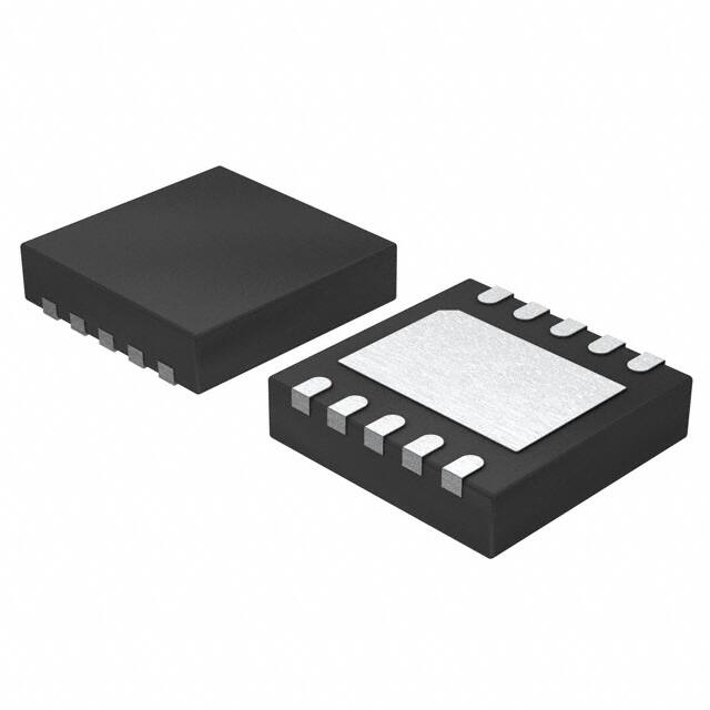
Low-profile 10-pin WSON Package (3 mm x 3 mm
x 0.8 mm)
True shutdown function by synchronous FET and
related circuitry ensures input and output isolation.
A programmable soft-start circuit allows the user to
limit the amount of inrush current during start-up. The
output voltage can be adjusted by external resistors.
The LM4510 features advanced short-circuit
protection to maximize safety during output to ground
short condition. During shutdown the feedback
resistors and the load are disconnected from the
input to prevent leakage current paths to ground.
Device Information(1)
PART NUMBER
2 Applications
•
•
•
•
•
•
The device's synchronous switching operation (no
external Schottky diode) at heavy-load, and nonsynchronous switching operation at light-load,
maximizes power efficiency.
LM4510
Organic LED Panel Power Supply
Charging Holster
White LED Backlight
USB Power Supply
Class D Audio Amplifier
Camera Flash LED Driver
space
Efficiency at VOUT = 16 V
100
VIN = 5.5V
VOUT 16.0V
SW
VOUT
PGND
FB
COUT
10 PF
COMP
RF2
RC
46.4k
AGND
CC1
2.2 nF
CC2
15 pF
20.5k
LOAD
EFFICIENCY (%)
SS
CS
10 nF
LM4500
LM4510
EN
VIN = 4.5V
90
RF1
240k
CIN
4.7 PF
3.00 mm x 3.00 mm
space
L = 4.7 PH
VIN
BODY SIZE (NOM)
WSON (10)
(1) For all available packages, see the orderable addendum at
the end of the datasheet.
Typical Application Circuit
VIN 2.7V ± 5.5V
PACKAGE
80
70
VIN = 3.6V
VIN = 2.7V
60
50
40
0 5 10 15 20 25 30 35 40 45 50 55 60 65 70
IOUT (mA)
1
An IMPORTANT NOTICE at the end of this data sheet addresses availability, warranty, changes, use in safety-critical applications,
intellectual property matters and other important disclaimers. PRODUCTION DATA.
�LM4510
SNVS533D – SEPTEMBER 2007 – REVISED NOVEMBER 2014
www.ti.com
Table of Contents
1
2
3
4
5
6
7
Features ..................................................................
Applications ...........................................................
Description .............................................................
Revision History.....................................................
Pin Configuration and Functions .........................
Specifications.........................................................
1
1
1
2
3
4
6.1
6.2
6.3
6.4
6.5
6.6
4
4
4
5
5
7
Absolute Maximum Ratings ......................................
Handling Ratings.......................................................
Recommended Operating Conditions.......................
Thermal Information ..................................................
Electrical Characteristics...........................................
Typical Characteristics ..............................................
Detailed Description ............................................ 10
7.1 Overview ................................................................. 10
7.2 Functional Block Diagram ....................................... 10
7.3 Feature Description................................................. 10
7.4 Device Functional Modes........................................ 11
8
Application and Implementation ........................ 13
8.1 Application Information............................................ 13
8.2 Typical Applications ................................................ 13
9 Power Supply Recommendations...................... 20
10 Layout................................................................... 20
10.1 Layout Guidelines ................................................. 20
10.2 Layout Example .................................................... 20
11 Device and Documentation Support ................. 21
11.1
11.2
11.3
11.4
Device Support......................................................
Trademarks ...........................................................
Electrostatic Discharge Caution ............................
Glossary ................................................................
21
21
21
21
12 Mechanical, Packaging, and Orderable
Information ........................................................... 21
4 Revision History
NOTE: Page numbers for previous revisions may differ from page numbers in the current version.
Changes from Revision C (May 2013) to Revision D
•
Added Device Information and Handling Rating tables, Feature Description, Device Functional Modes, Application
and Implementation, Power Supply Recommendations, Layout, Device and Documentation Support, and
Mechanical, Packaging, and Orderable Information sections; moved some curves to Application Curves section ............. 1
Changes from Revision B (May 2013) to Revision C
•
2
Page
Page
Changed layout of National Data Sheet to TI format ........................................................................................................... 19
Submit Documentation Feedback
Copyright © 2007–2014, Texas Instruments Incorporated
Product Folder Links: LM4510
�LM4510
www.ti.com
SNVS533D – SEPTEMBER 2007 – REVISED NOVEMBER 2014
5 Pin Configuration and Functions
WSON Package (DSC)
10 Pins
SW
1
10
VOUT
10
1
PGND
2
9
N/C
9
2
VIN
3
8
FB
8
3
EN
4
7
COMP
7
4
SS
5
6
AGND
6
5
Die-Attach Pad: GND
Die-Attach Pad: GND
Top View
Bottom View
Pin Functions
PIN
DESCRIPTION
NO.
NAME
TYPE
1
SW
A
Switch pin. Drain connections of both internal NMOS and PMOS devices.
2
PGND
G
Power ground
3
VIN
P
Analog and Power supply input. Input range: 2.7 V to 5.5 V.
4
EN
I
Enable logic input. HIGH= Enabled, LOW=Shutdown.
5
SS
A
Soft-start pin
6
AGND
G
Analog ground
7
COMP
A
Compensation network connection.
8
FB
A
Output voltage feedback connection.
9
N/C
10
VOUT
DAP
DAP
No internal connection.
A
Internal PMOS source connection for synchronous rectification.
Die Attach Pad thermal connection
Submit Documentation Feedback
Copyright © 2007–2014, Texas Instruments Incorporated
Product Folder Links: LM4510
3
�LM4510
SNVS533D – SEPTEMBER 2007 – REVISED NOVEMBER 2014
www.ti.com
6 Specifications
6.1 Absolute Maximum Ratings (1) (2) (3)
MIN
MAX
UNIT
VIN
−0.3
6.5
V
VOUT
−0.3
21
V
SW (4)
–0.3
VOUT+0.3
V
EN, SS, COMP FB
−0.3
6.5
V
PGND to AGND
−0.2
0.2
V
Continuous power dissipation (5)
Internally
Limited
Junction temperature (TJ-MAX)
150
Lead temperature (soldering, 10 sec) (6)
(1)
(2)
(3)
(4)
(5)
(6)
150
°C
260
°C
Absolute maximum ratings are limits beyond which damage to the device may occur. Recommended Operating Conditions are
conditions for which the device is intended to be functional. For specifications and test conditions, see the Electrical Characteristics.
All voltages are with respect to the potential at the GND pin.
If Military/Aerospace specified devices are required, please contact the Texas Instruments Sales Office/ Distributors for availability and
specifications.
This condition applies if VIN < VOUT. If VIN > VOUT, a voltage greater than VIN + 0.3 V should not be applied to the VOUT or SW pins.
The absolute maximum specification applies to DC voltage. An extended negative voltage limit of –1 V applies for a pulse of up to 1 µs,
and –2 V for a pulse of up to 40 ns. An extended positive voltage limit of 22 V applies for a pulse of up to 20 ns.
Internal thermal shutdown circuitry protects the device from permanent damage. Thermal shutdown engages at TJ= 150°C (Typ.) and
disengages at TJ= 140°C (Typ.).
For detailed soldering information and specifications, please refer to Application Note 1187: Leadless Leadframe Package (LLP)
(SNOI401).
6.2 Handling Ratings
Tstg
Storage temperature range
V(ESD)
(1)
(2)
Electrostatic discharge
MIN
MAX
UNIT
–65
150
°C
Human body model (HBM), per ANSI/ESDA/JEDEC JS001, all pins (1)
2
Charged device model (CDM), per JEDEC specification
JESD22-C101, all pins (2)
1000
Machine model
200
kV
V
V
JEDEC document JEP155 states that 500-V HBM allows safe manufacturing with a standard ESD control process.
JEDEC document JEP157 states that 250-V CDM allows safe manufacturing with a standard ESD control process.
6.3 Recommended Operating Conditions
MIN
MAX
UNIT
Supply voltage (VIN)
2.7
5.5
V
Junction temperature (TJ) (1)
−40
125
°C
18
V
Output voltage (VOUT)
(1)
4
In applications where high power dissipation and/or poor package thermal resistance is present, the maximum ambient temperature may
have to be derated. Maximum ambient temperature (TA-MAX) is dependent on the maximum operating junction temperature (TJ-MAX-OP =
125°C), the maximum power dissipation of the device in the application (PD-MAX), and the junction-to ambient thermal resistance of the
part/package in the application (RθJA), as given by the following equation: TA-MAX = TJ-MAX-OP – (RθJA × PD-MAX)
Submit Documentation Feedback
Copyright © 2007–2014, Texas Instruments Incorporated
Product Folder Links: LM4510
�LM4510
www.ti.com
SNVS533D – SEPTEMBER 2007 – REVISED NOVEMBER 2014
6.4 Thermal Information
LM4510
THERMAL METRIC (1)
DSC
UNIT
10 PINS
RθJA
Junction-to-ambient thermal resistance
RθJC(top)
Junction-to-case (top) thermal resistance
RθJB
Junction-to-board thermal resistance
22
ψJT
Junction-to-top characterization parameter
0.6
ψJB
Junction-to-board characterization parameter
22.1
RθJC(bot)
Junction-to-case (bottom) thermal resistance
3.8
(1)
36
48.3
°C/W
For more information about traditional and new thermal metrics, see the IC Package Thermal Metrics application report, SPRA953.
6.5 Electrical Characteristics
Unless otherwise stated the following conditions apply: VIN = 3.6 V, EN = 3.6 V, TJ = 25°C.
PARAMETER
TEST CONDITIONS
MIN (1)
2.7 V ≤ VIN ≤ 5.5 V
VFB
FB Pin Voltage
2.7 V ≤ VIN ≤ 5.5 V, −40°C ≤
TJ ≤ 125°C
IFB
FB Pin Bias Current (3)
−40°C ≤ TJ ≤ 125°C
NMOS Switch RDS(on)
ISW = 0.3 A
PMOS Switch RDS(on)
ISW = 0.3 A, VOUT = 10 V
RDS(on)
ICL
NMOS Switch Current Limit
IQ
1.24
1
IL
Shutdown Current
EN = 0 V
SW Leakage Current (3)
SW = 20 V
VOUT Bias Current (3)
VOUT = 20 V, −40°C ≤ TJ ≤
125°C
IVL
PMOS Switch Leakage
Current
SW = 0 V, VOUT = 20 V
fSW
Switching Frequency
DMAX
Maximum Duty Cycle
DMIN
Minimum Duty Cycle
Error Amplifier
Transconductance
Gm
Device Enable
EN
Threshold
Device Shutdown
(1)
(2)
(3)
0.050
1.5
0.45
1.1
0.9
1.1
1.2
1.8
0.002
0.050
µA
0.01
0.150
µA
90
50
150
0.001
0.85
0.100
1.2
µA
µA
MHz
94%
88%
15%
20%
130
−40°C ≤ TJ ≤ 125°C
A
2
FB = 0 V
FB = 0 V, −40°C ≤ TJ ≤ 125°C
Ω
mA
0.8
1
−40°C ≤ TJ ≤ 125°C
µA
2.5
VOUT = 20 V
IVOUT
V
1.7
EN = 3.6 V, FB > 1.29 V
EN = 3.6 V, FB > 1.29 V,
−40°C ≤ TJ ≤ 125°C
UNIT
1.29
EN = 3.6 V, FB = COMP,
−40°C ≤ TJ ≤ 125°C
Non-switching Current
MAX (1)
1.265
EN = 3.6 V, FB = COMP
Device Switching
TYP (2)
70
HIGH
200
µmho
0.81
HIGH, −40°C ≤ TJ ≤ 125°C
LOW
1.2
V
0.78
LOW, −40°C ≤ TJ ≤ 125°C
0.4
All room temperature limits are production tested, specified through statistical analysis or by design. All limits at −40°C ≤ TJ ≤ 125°C are
specified via correlation using standard Statistical Quality Control (SQC) methods. All limits are used to calculate Average Outgoing
Quality Level (AOQL).
Typical numbers are at 25°C and represent the most likely norm.
Current flows into the pin.
Submit Documentation Feedback
Copyright © 2007–2014, Texas Instruments Incorporated
Product Folder Links: LM4510
5
�LM4510
SNVS533D – SEPTEMBER 2007 – REVISED NOVEMBER 2014
www.ti.com
Electrical Characteristics (continued)
Unless otherwise stated the following conditions apply: VIN = 3.6 V, EN = 3.6 V, TJ = 25°C.
PARAMETER
TEST CONDITIONS
MIN (1)
0 < EN < 3.6 V
IEN
EN Pin Bias Current
Feedback Fault Protection
ON Threshold, −40°C ≤ TJ ≤
125°C
8
18
Input Undervoltage Lockout
17
ISS
(4)
6
Soft-Start Pin Current (4)
V
20
2.5
ON Threshold, −40°C ≤ TJ ≤
125°C
2.65
OFF Threshold
OFF Threshold, −40°C ≤ TJ ≤
125°C
V
2.35
2.1
11.3
−40°C ≤ TJ ≤ 125°C
µA
20.7
18.7
ON Threshold
UVLO
UNIT
19.7
OFF Threshold
OFF Threshold, −40°C ≤ TJ ≤
125°C
MAX (1)
3.2
0 < EN < 3.6 V, −40°C ≤ TJ ≤
125°C
ON Threshold
FB Fault
Protection
TYP (2)
9
15
µA
Current flows out of the pin.
Submit Documentation Feedback
Copyright © 2007–2014, Texas Instruments Incorporated
Product Folder Links: LM4510
�LM4510
www.ti.com
SNVS533D – SEPTEMBER 2007 – REVISED NOVEMBER 2014
6.6 Typical Characteristics
LM4510SD, Circuit of Figure 18, (L = 4.7 µH, COILCRAFT, DO3316-472ML; CIN = 4 .7 µF, TDK, C2012X5R0J475K; COUT =
10 µF, AVX, 12103D106KAT2A; CS = 10 nF, TDK, C1608C0G1E103J; CC1 = 2.2 nF, Taiyo Yuden, TMK107SD222JA-T; RC =
46.4 kΩ, Yageo, 9t06031A4642FBHFT), VIN = 3.6 V, VOUT = 16 V, TA = 25°C, unless otherwise noted.
2.8
1200
2.6
1000
2.4
RDS(ON) (mÖ)
IQ (mA)
2.2
2.0
1.8
1.6
IQ at -35°C
1.4
800
PMOS VIN = 3.6V
600
400
IQ at 85°C
1.2
200
NMOS VIN = 3.6V
IQ at 25°C
1.0
0.8
2.8
3.2
3.6
4
4.4
5.6
5.2
4.8
0
-40
-20
0
VIN (V)
Figure 1. Switching Quiescent Current vs VIN
17.02
-35°C
80
100
IOUT = 10 mA
17.00
350
16.98
300
25°C
VOUT (V)
IOUT MAX (mA)
60
17.04
400
250
200
150
IOUT = 50 mA
16.96
16.94
16.92
IOUT = 100 mA
16.90
16.88
100
90°C
16.86
50
2
2.5
3
3.5
4
4.5
5
5.5
16.84
-60 -40 -20
6
VIN (V)
20
40
60
80
100
Figure 4. Output Voltage vs Temperature (VOUT = 17 V)
1.03
16.24
1.02
0
TEMPERATURE (°C)
Figure 3. Load Capability vs VIN (VOUT = 16 V )
Frequency at VIN = 4.5V
VIN = 5.5V
VIN = 4.5V
16.22
1.01
1.00
VIN = 3.6V
16.20
0.99
VOUT (V)
FREQUENCY (MHz)
40
Figure 2. RDS(on) vs Temperature at VIN= 3.6 V
450
0
20
TEMPERATURE (°C)
0.98
0.97 Frequency at VIN = 3.6V
16.18
16.16
0.96
16.14
0.95
0.94
Frequency at VIN = 2.7V
0.93
0.92
-40
16.12
VIN = 2.7V
VIN = 3.0V
-20
0
20
40
60
80
16.10
0
100
20
40
60
80
IOUT (mA)
TEMPERATURE (°C)
Figure 5. Switching Frequency vs Temperature
Figure 6. Load Regulation (VOUT = 16 V)
Submit Documentation Feedback
Copyright © 2007–2014, Texas Instruments Incorporated
Product Folder Links: LM4510
7
�LM4510
SNVS533D – SEPTEMBER 2007 – REVISED NOVEMBER 2014
www.ti.com
Typical Characteristics (continued)
LM4510SD, Circuit of Figure 18, (L = 4.7 µH, COILCRAFT, DO3316-472ML; CIN = 4 .7 µF, TDK, C2012X5R0J475K; COUT =
10 µF, AVX, 12103D106KAT2A; CS = 10 nF, TDK, C1608C0G1E103J; CC1 = 2.2 nF, Taiyo Yuden, TMK107SD222JA-T; RC =
46.4 kΩ, Yageo, 9t06031A4642FBHFT), VIN = 3.6 V, VOUT = 16 V, TA = 25°C, unless otherwise noted.
5.030
16.25
IOUT = 30 mA
5.028
VIN = 4.2V
16.23
5.024
5.022
5.020
5.018
IOUT = 50 mA
IOUT = 10 mA
VOUT (V)
VOUT (V)
5.026
VIN = 3.6V
VIN = 3.0V
16.21
IOUT = 70 mA
16.19
16.17
5.016
5.014
0
50
100
150
200
250
16.15
2.5
300
IOUT (mA)
3.0
3.5
4.0
4.5
5.0
5.5
6.0
VIN (V)
Figure 7. Load Regulation (VOUT = 5 V)
Figure 8. Line Regulation (VOUT = 16 V)
5.040
5.035
VOUT (V)
5.030
IOUT = 10 mA
5.025
5.020
5.015
IOUT = 240 mA
IOUT = 120 mA
5.010
2.5 2.7 2.9 3.1 3.3 3.5 3.7 3.9 4.1 4.3 4.5
VIN (V)
8
Figure 9. Line Regulation (VOUT = 5 V)
Figure 10. Line Transient Response (VOUT = 16 V)
Figure 11. Load Transient Response (VOUT = 16 V)
Figure 12. Short Circuit Response (VOUT = 16 V)
Submit Documentation Feedback
Copyright © 2007–2014, Texas Instruments Incorporated
Product Folder Links: LM4510
�LM4510
www.ti.com
SNVS533D – SEPTEMBER 2007 – REVISED NOVEMBER 2014
Typical Characteristics (continued)
LM4510SD, Circuit of Figure 18, (L = 4.7 µH, COILCRAFT, DO3316-472ML; CIN = 4 .7 µF, TDK, C2012X5R0J475K; COUT =
10 µF, AVX, 12103D106KAT2A; CS = 10 nF, TDK, C1608C0G1E103J; CC1 = 2.2 nF, Taiyo Yuden, TMK107SD222JA-T; RC =
46.4 kΩ, Yageo, 9t06031A4642FBHFT), VIN = 3.6 V, VOUT = 16 V, TA = 25°C, unless otherwise noted.
Figure 13. Output Voltage Ripple (VOUT = 16 V, IOUT = 90 mA)
Figure 14. Output Voltage Ripple (VOUT = 5 V, IOUT = 100 mA)
Submit Documentation Feedback
Copyright © 2007–2014, Texas Instruments Incorporated
Product Folder Links: LM4510
9
�LM4510
SNVS533D – SEPTEMBER 2007 – REVISED NOVEMBER 2014
www.ti.com
7 Detailed Description
7.1 Overview
LM4510 is a peak current-mode, fixed-frequency PWM boost regulator that employs both Synchronous and NonSynchronous Switching.
The DC/DC regulator regulates the feedback output voltage providing excellent line and load transient response.
The operation of the LM4510 can best be understood by referring to the Block Diagram.
7.2 Functional Block Diagram
EN
VIN
SS
VOUT
10 uA
S/D
Feedback Fault Protection
+
-
TSD
UVP
REF
OSC
BODY DIODE CTRL and TRUE S/D
UVP
+
-
LOGIC
SCP
CURRENT
LIMIT
Current
Sense
Ramp
RESET
SYNC/NONSYNC
S Q
PWM
+
BG
SET
R Q
SW
BG
COMP
+
EAMP
REF
FB
AGND
PGND
7.3 Feature Description
7.3.1 Short Circuit Protection
When VOUT goes down to VIN–0.7V (typ.), the device stops switching due to the short-circuit protection circuitry
and the short-circuit output current is limited to IINIT_CHARGE.
10
Submit Documentation Feedback
Copyright © 2007–2014, Texas Instruments Incorporated
Product Folder Links: LM4510
�LM4510
www.ti.com
SNVS533D – SEPTEMBER 2007 – REVISED NOVEMBER 2014
Feature Description (continued)
7.3.2 Feedback Fault Protection
The LM4510 features unique Feedback Fault Protection to maximize safety when the feedback resistor is not
properly connected to a circuit or the feedback node is shorted directly to ground.
Feedback fault triggers VOUT monitoring. During monitoring, if VOUT reaches a protection level, the device shuts
down. When the feedback network is reconnected and VOUT is lower than the OFF threshold level of Feedback
Fault Protection, VOUT monitoring stops. VOUT is then regulated by the control loop.
7.3.3 Input Undervoltage Lock-Out
The LM4510 has dedicated circuitry to protect the IC and the external components when the battery voltage is
lower than the preset threshold. This undervoltage lock-out with hysteresis prevents malfunctions during start-up
or abnormal power off.
7.3.4 Thermal Shutdown
If the die temperature exceeds 150°C (typ.), the thermal protection circuitry shuts down the device. The switches
remain off until the die temperature is reduced to approximately 140°C (typ.).
7.4 Device Functional Modes
7.4.1 Non-Synchronous Operation
The device operates in Non-synchronous Mode at light load (IOUT < 10 mA) or when output voltage is lower than
10 V (typ.). At light load, LM4510 automatically changes its switching operation from 'Synchronous' to 'NonSynchronous' depending on VIN and L. Non-Synchronous operation at light load maximizes power efficiency by
reducing PMOS driving loss.
7.4.2 Operation in Synchronous Continuous Conduction Mode (Cycle 1, Cycle 2)
VSW1
VOUT
PMOS
NMOS
+GND
PWM
RLOAD
COUT
Figure 15. Schematic of Synchronous Boost Converter
Synchronous boost converter is shown in Figure 15. At the start of each cycle, the oscillator sets the driver logic
and turns on the NMOS power device and turns off the PMOS power device.
7.4.2.1 Cycle 1 Description
Refer to Figure 16. NMOS switch turn-on → Inductor current increases and flows to GND.
PMOS switch turn-off → Isolate VOUT from SW → Output capacitor supplies load current.
OFF
++
--
ON
Figure 16. Equivalent Circuit During Cycle 1
Submit Documentation Feedback
Copyright © 2007–2014, Texas Instruments Incorporated
Product Folder Links: LM4510
11
�LM4510
SNVS533D – SEPTEMBER 2007 – REVISED NOVEMBER 2014
www.ti.com
Device Functional Modes (continued)
During operation, EAMP output voltage (VCOMP) increases for larger loads and decreases for smaller loads.
When the sum of the ramp compensation and the sensed NMOS current reaches a level determined by the
EAMP output voltage, the PWM COMP resets the logic, turning off the NMOS power device and turning on the
PMOS power device.
7.4.2.2 Cycle 2 Description
Refer to Figure 17. NMOS Switch turn-off → PMOS Switch turn-on→ Inductor current decreases and flows
through PMOS → Inductor current recharges output capacitor and supplies load current.
ON
OFF
Figure 17. Equivalent Circuit During Cycle 2
After the switching period the oscillator then sets the driver logic again repeating the process.
12
Submit Documentation Feedback
Copyright © 2007–2014, Texas Instruments Incorporated
Product Folder Links: LM4510
�LM4510
www.ti.com
SNVS533D – SEPTEMBER 2007 – REVISED NOVEMBER 2014
8 Application and Implementation
NOTE
Information in the following applications sections is not part of the TI component
specification, and TI does not warrant its accuracy or completeness. TI’s customers are
responsible for determining suitability of components for their purposes. Customers should
validate and test their design implementation to confirm system functionality.
8.1 Application Information
The LM4510 shuts down when the EN pin is low. In this mode the feedback resistors and the load are
disconnected from the input in order to avoid leakage current flow and to allow the output voltage to drop to 0 V.
The LM4510 turns on when EN is high. There is an internal pull-down resistor on the EN pin so the device is in a
normally off state.
8.2 Typical Applications
8.2.1 2.7 V to 5.5 V Input with a 16 V Output
L = 4.7 PH
VIN 2.7V ± 5.5V
VOUT 16.0V
VIN
SW
VOUT
RF1
240k
SS
CS
10 nF
PGND
LM4500
LM4510
EN
CIN
4.7 PF
FB
COUT
10 PF
COMP
AGND
RF2
LOAD
20.5k
RC
46.4k
CC2
CC1 15 pF
2.2 nF
Figure 18. Typical Application Circuit for Normal DC/DC
8.2.1.1 Design Requirements
The LM4510 is designed to operate up to 75 mA at 2.7 V input and 350 mA at 5.5 V input to output 16 V. In any
case, it is recommended to avoid starting up the device at minimum input voltage and maximum load. Special
attention must be taken to avoid operating near thermal shutdown condition. A simple calculation can be used to
determine the power dissipation at the operating condition. PD-MAX = (TJ-MAX-OP – TA-MAX)/RθJA(TJ-MAX-OP = 125°C).
8.2.1.2 Detailed Design Procedure
8.2.1.2.1 Adjusting Output Voltage
The output voltage is set using the feedback pin and a resistor voltage divider (RF1, RF2) connected to the output
as shown in Figure 18.
The ratio of the feedback resistors sets the output voltage.
RF2 Selection First of all choose a value for RF2 generally between 10 kΩ and 25 kΩ.
RF1 Selection Calculate RF1 using Equation 1:
Submit Documentation Feedback
Copyright © 2007–2014, Texas Instruments Incorporated
Product Folder Links: LM4510
13
�LM4510
SNVS533D – SEPTEMBER 2007 – REVISED NOVEMBER 2014
www.ti.com
Typical Applications (continued)
R F1 = (
VO
VFB
- 1) x RF2 [:]
(1)
Table 1 gives suggested component values for several typical output voltages.
Table 1. Suggested Component Values for Different Output Voltages
OUTPUT VOLTAGE (V)
RF2 (kΩ)
RF1 (kΩ)
RC (kΩ)
CC1 (nF)
16
20.5
240
46.4
2.2
12
20.5
174
46.4
2.2
5
20.5
60.4
46.4
2.2
3.3
20.5
33
46.4
2.2
8.2.1.2.2 Maximum Output Current
When the output voltage is set at different level, it is important to know the maximum load capability. By first
order estimation, IOUT(MAX) can be estimated by Equation 2:
1.32 x VIN - 2.79
IOUT_Max =
VOUT
[A]
(2)
8.2.1.2.3 Inductor Selection
The larger value inductor makes lower peak inductor current and reduces stress on internal power NMOS.
On the other hand, the smaller value inductor has smaller outline, lower DCR and a higher current capacity.
Generally a 4.7-μH to 15-μH inductor is recommended.
8.2.1.2.4 IL_AVE Check
The average inductor current is given by Equation 3:
I L_ AVE =
VIN
I OUT
[ A ], D' =
K x D¿
VOUT
(3)
Where IOUT is output current, η is the converter efficiency of the total driven load and D’ is the off duty cycle of the
switching regulator.
Inductor DC current rating (40°C temperature rise) should be more than the average inductor current at worst
case.
ΔI Define
The inductor ripple current is given by Equation 4:
'IL =
VIN x D
L x fSW
[ A ], D =
VOUT - VIN
VOUT
(4)
Where D is the on-duty cycle of the switching regulator. A common choice is to set ΔIL to about 30% of IL_AVE.
IL_PK≤ ICL Check & IMIN Define
The peak inductor current is given by Equation 5:
14
Submit Documentation Feedback
Copyright © 2007–2014, Texas Instruments Incorporated
Product Folder Links: LM4510
�LM4510
www.ti.com
SNVS533D – SEPTEMBER 2007 – REVISED NOVEMBER 2014
'IL
[ A]
2
IL _ pk = IL _ AVE +
IL _ pk =
IOUT
K x D¿
+
VIN x D
2L x fSW
[ A]
(5)
To prevent loss of regulation, ensure that the NMOS power switch current limit is greater than the worst-case
peak inductor current in the target application.
Also make sure that the inductor saturation current is greater than the peak inductor current under the worst-case
load transient, high ambient temperature and start-up conditions. Refer to Table 2 for suggested inductors.
Table 2. Suggested Inductors and Their Suppliers
MODEL
VENDOR
DIMENSIONS LxWxH (mm)
D.C.R (max)
DO3314-472ML
COILCRAFT
3.3mm x 3.3mm x 1.4mm
320 mΩ
DO3316P-472ML
COILCRAFT
12.95mm x 9.4mm x 5.4mm
18 mΩ
8.2.1.2.5 Input Capacitor Selection
Due to the presence of an inductor, the input current waveform is continuous and triangular. So the input
capacitor is less critical than output capacitor in boost applications. Typically, a 4.7-μF to 10-μF ceramic input
capacitor is recommended on the VIN pin of the IC.
ICIN_RMS Check
The RMS current in the input capacitor is given by Equation 6:
ICIN_ RMS =
'IL
12
[ A]
(6)
The input capacitor should be capable of handling the RMS current.
8.2.1.2.6 Output Capacitor Selection
The output capacitor in a boost converter provides all the output current when the switch is closed and the
inductor is charging. As a result, it sees very large ripple currents.
A ceramic capacitor of value 4.7 μF to 10 μF is recommended at the output. If larger amounts of capacitance are
desired for improved line support and transient response, tantalum capacitors can be used.
ICOUT_RMS Check
The RMS current in the output capacitor is given by Equation 7:
º
»
¼
I COUT_RMS =
2
2
(1 - D ) I OUT
' IL
D
+
2
12
(1 - D )
º [ A]
»
¼
(7)
The output capacitor should be capable of handling the RMS current.
The ESR and ESL of the output capacitor directly control the output ripple. Use capacitors with low ESR and ESL
at the output for high efficiency and low ripple voltage. The output capacitor also affects the soft-start time (See
Soft-Start Function and Soft-Start Capacitor Selection). Table 3 shows suggested input and output capacitors.
Submit Documentation Feedback
Copyright © 2007–2014, Texas Instruments Incorporated
Product Folder Links: LM4510
15
�LM4510
SNVS533D – SEPTEMBER 2007 – REVISED NOVEMBER 2014
www.ti.com
Table 3. Suggested CIN and COUT Capacitors and Their Suppliers
MODEL
TYPE
VENDOR
VOLTAGE
RATING
CASE SIZE
INCH (mm)
4.7 µF for CIN
C2012X5R0J475
Ceramic, X5R
TDK
6.3 V
0805 (2012)
GRM21BR60J475
Ceramic, X5R
muRata
6.3 V
0805 (2012)
JMK212BJ475
Ceramic, X5R
Taiyo-Yuden
6.3 V
0805 (2012)
C2012X5R0J475K
Ceramic, X5R
TDK
6.3 V
0603 (1608)
TMK316BJ106KL
Ceramic, X5R
Taiyo-Yuden
25 V
1206 (3216)
12103D106KAT2A
Ceramic, X5R
AVX
25 V
1210 (3225)
10 µF for COUT
8.2.1.2.7 Soft-Start Function and Soft-Start Capacitor Selection
The LM4510 has a soft-start pin that can be used to limit the input inrush current. Connect a capacitor from SS
pin to GND to set the soft-start period. Figure 19 describes the soft start process.
• Initial charging period: When the device is turned on, the control circuitry linearly regulating initial charge
current charges VOUT by limiting the inrush current.
• Soft-start period: After VOUT reaches VIN –0.7 V (typ.), the device starts switching and the CS is charged at a
constant current of 11 μA, ramping up to VIN. This period ends when VSS reaches VFB. CS should be large
enough to ensure soft-start period ends after CO is fully charged.
During the initial charging period, the required load current must be smaller than the initial charge current to
ensure VOUT reaches VIN –0.7 V (typ.).
VEN
VSS = VIN
VSS = VFB
VSS
appropriate VOUT
VOUT = VIN - 0.7V
Normal Switching
Operation
Soft-Start
Switching Period
Linear Charging
Period
Shutdown
VOUT
Figure 19. Soft-Start Timing Diagram
CS Selection
The soft-start time without load can be estimated as:
t SS =
COUT x ( VIN - 0.7)
IINIT _ CHARGE
+
CS x VFB
ISS _ CHARGE
[sec]
(8)
Where the IINIT_CHARGE is Initial Charging Current depending on VIN and ISS_CHARGE (11 μA (typ.). Also, when
selecting the fuse current rating, make sure the value is higher than the initial charging current.
16
Submit Documentation Feedback
Copyright © 2007–2014, Texas Instruments Incorporated
Product Folder Links: LM4510
�LM4510
www.ti.com
SNVS533D – SEPTEMBER 2007 – REVISED NOVEMBER 2014
8.2.1.2.8 Compensation Component Selection
The LM4510 provides a compensation pin COMP to customize the voltage loop feedback. It is recommended
that a series combination of RC and CC1 be used for the compensation network, as shown in the typical
application circuit. In addition, CC2 is used for compensating high frequency zeros.
The series combination of RC and CC1 introduces a pole-zero pair according to Equation 9:
fPC =
1
[ Hz]
2S(RC + RO) CC1
f ZC =
1
[ Hz]
2SRCCC1
(9)
In addition, CC2 introduces a pole according to Equation 10:
fPC2 =
1
[ Hz]
2S(RC // R O ) CC2
(10)
Where RO is the output impedance of the error amplifier, approximately 1 MΩ, and amplifier voltage gain is
typically 200 V/V depending on temperature and VIN.
Refer to Table 4 for suggested soft start capacitor and compensation components.
Table 4. Suggested CS and Compensation Components
MODEL
TYPE
VENDOR
VOLTAGE RATING
CASE SIZE
INCH (mm)
(CS) C1608C0G1E103J
Ceramic, X5R
TDK
6.3 V
603 (1608)
(C1)TMK107SD222JA-T
Ceramic, X5R
Taiyo Yuden
25 V
603 (1608)
(RC) 9t06031A4642FBHFT
Resistor
Yageo Corporation
1/10 W
603 (1608)
Submit Documentation Feedback
Copyright © 2007–2014, Texas Instruments Incorporated
Product Folder Links: LM4510
17
�LM4510
SNVS533D – SEPTEMBER 2007 – REVISED NOVEMBER 2014
www.ti.com
8.2.1.3 Application Curves
100
100
VIN = 3.6V
VIN = 4.5V
VIN = 5.5V
80
70
VIN = 4.5V
90
EFFICIENCY (%)
EFFICIENCY (%)
90
VIN = 3.6V
VIN = 2.7V
60
80
VIN = 3.0V
70
VIN = 5.5V
60
50
50
40
0 5 10 15 20 25 30 35 40 45 50 55 60 65 70
40
0
10 20 30 40 50 60 70 80 90 100
IOUT (mA)
IOUT (mA)
Figure 20. Efficiency vs Output Current (VOUT = 16 V)
85
Figure 21. Efficiency vs Output Current (VOUT = 12 V)
VIN = 4.2V
EFFICIENCY (%)
80
75
VIN = 3.6V
70
65
VIN = 3.0V
60
55
50
0
40
80
120
160
200
240
280
IOUT = (mA)
Figure 22. Efficiency vs Output Current (VOUT = 5 V, L=
DO3314-472ML)
Figure 23. Start Up (VOUT = 16 V, RLOAD = 530 Ω)
Figure 24. Shut Down (VOUT = 16 V, RLOAD = 940 Ω)
18
Submit Documentation Feedback
Copyright © 2007–2014, Texas Instruments Incorporated
Product Folder Links: LM4510
�LM4510
www.ti.com
SNVS533D – SEPTEMBER 2007 – REVISED NOVEMBER 2014
8.2.2 Flash and Torch Application
LM4510 can be configured to drive white LEDs for the flash and torch functions. The flash/torch can be set up
with the circuit shown in Figure 25 by using the resistor RT to determine the current in Torch Mode and RF to
determine the current in Flash Mode. The amount of current can be estimated using Equation 11:
I Torch =
IFlash =
VFB
RT
[A]
VFB
R T // RF
[ A]
(11)
L = 4.7 éH
VIN
EN
Battery or
Power Source
CIN
SW
Everlight
47-23UWD/TR8
VOUT
LM4510
COUT
4.7 éF
FB
SS
CS
10 nF
COMP
10 éF
RC
46.6k
PGND
AGND
RT
50Ö
RF
12.4Ö
CC
2.2 nF
Pull high for TORCH
Pull high for FLASH
Figure 25. Typical Application Circuit for Flash/Torch
8.2.2.1 Design Requirements
See Design Requirements.
8.2.2.2 Detailed Design Procedure
See Detailed Design Procedure.
8.2.2.3 Application Curve
See Application Curves.
Submit Documentation Feedback
Copyright © 2007–2014, Texas Instruments Incorporated
Product Folder Links: LM4510
19
�LM4510
SNVS533D – SEPTEMBER 2007 – REVISED NOVEMBER 2014
www.ti.com
9 Power Supply Recommendations
The power supply for the applications using the LM4510 device should be big enough considering output power
and efficiency at given input voltage condition. Minimum current requirement condition is (VOUT * IOUT)/(VIN *
efficiency) and approximately 20 - 30% higher than this value is recommended
10 Layout
10.1 Layout Guidelines
High frequency switching regulators require very careful layout of components in order to get stable operation
and low noise. All components must be as close as possible to the LM4510 device. Refer to Figure 26 as an
example. Some additional guidelines to be observed:
1. CIN must be placed close to the device and connected directly from VIN to PGND pins. This reduces copper
trace resistance, which affects the input voltage ripple of the device. For additional input voltage filtering,
typically a 0.1 uF bypass capacitor can be placed between VIN and AGND. This bypass capacitor should be
placed near the device closer than CIN.
2. COUT must also be placed close to the device and connected directly from VOUT to PGND pins. Any copper
trace connections for the COUT capacitor can increase the series resistance, which directly affects output
voltage ripple and makes noise during output voltage sensing.
3. All voltage-sensing resistors (RF1, RF2) should be kept close to the FB pin to minimize copper trace
connections that can inject noise into the system. The ground connection for the voltage-sensing resistor
should be connected directly to the AGND pin.
4. Trace connections made to the inductor should be minimized to reduce power dissipation, EMI radiation and
increase overall efficiency. Also poor trace connection increases the ripple of SW.
5. CS, CC1, CC2, RC must be placed close to the device and connected to AGND.
6. The AGND pin should connect directly to the ground. Not connecting the AGND pin directly, as close to the
chip as possible, may affect the performance of the LM4510 and limit its current driving capability. AGND
and PGND should be separate planes and should be connected at a single point.
7. For better thermal performance, DAP should be connected to ground, but cannot be used as the primary
ground connection. The PC board land may be modified to a "dog bone" shape to reduce SON thermal
impedance. For detail information, refer to Application Note AN-1187.
10.2 Layout Example
Figure 26. Evaluation Board Layout
20
Submit Documentation Feedback
Copyright © 2007–2014, Texas Instruments Incorporated
Product Folder Links: LM4510
�LM4510
www.ti.com
SNVS533D – SEPTEMBER 2007 – REVISED NOVEMBER 2014
11 Device and Documentation Support
11.1 Device Support
11.1.1 Third-Party Products Disclaimer
TI'S PUBLICATION OF INFORMATION REGARDING THIRD-PARTY PRODUCTS OR SERVICES DOES NOT
CONSTITUTE AN ENDORSEMENT REGARDING THE SUITABILITY OF SUCH PRODUCTS OR SERVICES
OR A WARRANTY, REPRESENTATION OR ENDORSEMENT OF SUCH PRODUCTS OR SERVICES, EITHER
ALONE OR IN COMBINATION WITH ANY TI PRODUCT OR SERVICE.
11.2 Trademarks
All trademarks are the property of their respective owners.
11.3 Electrostatic Discharge Caution
These devices have limited built-in ESD protection. The leads should be shorted together or the device placed in conductive foam
during storage or handling to prevent electrostatic damage to the MOS gates.
11.4 Glossary
SLYZ022 — TI Glossary.
This glossary lists and explains terms, acronyms, and definitions.
12 Mechanical, Packaging, and Orderable Information
The following pages include mechanical, packaging, and orderable information. This information is the most
current data available for the designated devices. This data is subject to change without notice and revision of
this document. For browser-based versions of this data sheet, refer to the left-hand navigation.
Submit Documentation Feedback
Copyright © 2007–2014, Texas Instruments Incorporated
Product Folder Links: LM4510
21
�PACKAGE OPTION ADDENDUM
www.ti.com
10-Dec-2020
PACKAGING INFORMATION
Orderable Device
Status
(1)
Package Type Package Pins Package
Drawing
Qty
Eco Plan
(2)
Lead finish/
Ball material
MSL Peak Temp
Op Temp (°C)
Device Marking
(3)
(4/5)
(6)
LM4510SD/NOPB
ACTIVE
WSON
DSC
10
1000
RoHS & Green
NIPDAU | SN
Level-1-260C-UNLIM
-40 to 85
L4510
LM4510SDX/NOPB
ACTIVE
WSON
DSC
10
4500
RoHS & Green
NIPDAU | SN
Level-1-260C-UNLIM
-40 to 85
L4510
(1)
The marketing status values are defined as follows:
ACTIVE: Product device recommended for new designs.
LIFEBUY: TI has announced that the device will be discontinued, and a lifetime-buy period is in effect.
NRND: Not recommended for new designs. Device is in production to support existing customers, but TI does not recommend using this part in a new design.
PREVIEW: Device has been announced but is not in production. Samples may or may not be available.
OBSOLETE: TI has discontinued the production of the device.
(2)
RoHS: TI defines "RoHS" to mean semiconductor products that are compliant with the current EU RoHS requirements for all 10 RoHS substances, including the requirement that RoHS substance
do not exceed 0.1% by weight in homogeneous materials. Where designed to be soldered at high temperatures, "RoHS" products are suitable for use in specified lead-free processes. TI may
reference these types of products as "Pb-Free".
RoHS Exempt: TI defines "RoHS Exempt" to mean products that contain lead but are compliant with EU RoHS pursuant to a specific EU RoHS exemption.
Green: TI defines "Green" to mean the content of Chlorine (Cl) and Bromine (Br) based flame retardants meet JS709B low halogen requirements of