User's Guide
SNVA239B – December 2007 – Revised April 2013
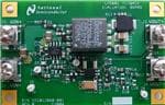
AN-1630 LM5001 Non-Isolated Flyback Evaluation Board
1
Introduction
The LM5001 non-isolated flyback evaluation board is designed to provide the design engineer with a fully
functional non-isolated flyback power converter based on Current Mode Control to evaluate the LM5001
switching regulator IC. The evaluation board provides a 5V output with 1A current capability. The input
voltage ranges from 16V to 42V. The design operates at 250KHz, a good compromise between
conversion efficiency and solution size. The printed circuit board consists of 2 layers of 2 ounce copper on
FR4 material with a thickness of 0.062 inches. This application note contains the evaluation board
schematic, Bill-of-Materials (BOM) and a quick setup procedure. Refer to the LM5001 datasheet for
complete circuit design information. For complete circuit design information, see LM5001 High Voltage
Switch Mode Regulator (SNVS484).
The performance of the evaluation board is:
• Input Range: 16 to 42V
• Output Voltage: 5V, ±2%
• Output Current: 0 to 1A
• Frequency of Operation: 250 kHz
• Board Size: 2.75 × 1.75 × 0.6 inches
• Load Regulation: 0.1%
• Line Regulation: 0.1%
• Over Current Limiting
All trademarks are the property of their respective owners.
SNVA239B – December 2007 – Revised April 2013
Submit Documentation Feedback
AN-1630 LM5001 Non-Isolated Flyback Evaluation Board
Copyright © 2007–2013, Texas Instruments Incorporated
1
�Evaluation Board Schematic
2
www.ti.com
Evaluation Board Schematic
T1
VCC
VIN = 16V ± 42V
J1
R5
20
D1
LPRI = 160 éH
5 8:3:2
R12
10
C11
470 pF
VOUT = +5V
IOUT = 1A
J3
6,7
C1
2.2 éF
C2
2.2 éF
4
3
J2
GND
R6
8.06k
R1
60.4k
J7
ENABLE
C4
0.01 éF
D4
8,9
R11
0
R2
10
C3
0.1 éF
R4
52.3k
2
VIN
8
EN
5
RT
4
GND
R9
10.2k
C10
220 pF
C9
4700 pF
1
SW
7
COMP
6
FB
3
VCC
LM5001
R3
6.04k
J4
C7
0.01 éF 2
U1
SYNC
C14
1 éF
C13
47 éF
D2
C5
100 pF
J6
C12
47 éF
R8
13.0k
VCC
R10
3.40k
C6
1 éF
R7
100k
OPTIONAL
SOFT-START
J5
D3
C8
10 éF
GND
C19
0
J8
IGND
Figure 1. Evaluation Board Schematic
2
AN-1630 LM5001 Non-Isolated Flyback Evaluation Board
SNVA239B – December 2007 – Revised April 2013
Submit Documentation Feedback
Copyright © 2007–2013, Texas Instruments Incorporated
�Powering and Loading Considerations
www.ti.com
3
Powering and Loading Considerations
Read this entire section prior to attempting to power the evaluation board.
3.1
Quick Setup Procedure
Step 1: Set the input source current limit to 1A. Turn off the input source. Connect the positive output of
the input source to J1 and the negative output to J2.
Step 2: Connect the load, with 1A capability, to J3 for the positive connection and J4 for the negative
connection.
Step 3: The ENABLE pin, J7, should be left open for normal operation.
Step 4: Set the input source voltage to 28V and the load to 0.1A. The load voltage should be in regulation
with a nominal 5V output.
Step 5: Slowly increase the load while monitoring the load voltage at J3 and J4. It should remain in
regulation with a nominal 5V output as the load is increased up to 1 Amp.
Step 6: Slowly sweep the input source voltage from 16V to 42V. The load voltage should remain in
regulation with a nominal 5V output.
Step 7: Temporally short the ENABLE pin (J7) to GND (J5) to check the shutdown function.
Step 8: Increase the load beyond the normal range to check current limiting while the input source is set
to 28V. The output current should limit at approximately 1.9A. The input source current limit should be
increased for this step. Fan cooling is critical during this step.
3.2
AIr Flow
Prolonged operation at full power and high ambient temperature will cause the thermal shutdown circuit
within the regulator IC to activate. A fan with a minimum of 200 LFM should always be provided.
3.3
Powering Up
Using the ENABLE pin (J7) provided will allow powering up the input source with the current level set low.
It is suggested that the load power be kept low during the first power up. Set the current limit of the input
source to provide about 1.5 times the anticipated wattage of the load. As you remove the connection from
the ENABLE pin to GND (J5), immediately check for 5 volts at the output.
A quick efficiency check is the best way to confirm that everything is operating properly. If something is
amiss you can be reasonably sure that it will affect the efficiency adversely. Few parameters can be
incorrect in a switching power supply without creating losses and potentially damaging heat.
3.4
Over Current Protection
The evaluation board is configured with cycle-by-cycle over-current protection. This function is completely
contained in the LM5001. The Primary current is limited to approximately 1A. This equates to about 1.4A
load current when the input voltage is 16V, and about 2.1A load current when the input is 42V. The
thermal stress on various circuit components is quite severe while in an overloaded condition, therefore
limit the duration of the overload and provide sufficient cooling (airflow).
3.5
Synchronization
A SYNC pin (J6) has been provided on the evaluation board. This pin can be used to synchronize the
regulator to an external clock or multiple evaluation boards can be synchronized together by connecting
their SYNC pins together. For complete information, see LM5001 High Voltage Switch Mode Regulator
(SNVS484).
SNVA239B – December 2007 – Revised April 2013
Submit Documentation Feedback
AN-1630 LM5001 Non-Isolated Flyback Evaluation Board
Copyright © 2007–2013, Texas Instruments Incorporated
3
�Flyback Topology
www.ti.com
4
Flyback Topology
4.1
Flyback Transformer
Two things need to be considered when specifying a Flyback transformer to a magnetics manufacturer
(Coilcraft, Pulse Engineering, Cooper-Coiltronics, and so on), the turns ratio to determine the duty cycle D
(MOSFET on time compared to the switching period) and the primary inductance (LPRI) to determine the
current sense ramp for current mode control.
To start, the primary inductance in Continuous Current Mode (CCM) is designed to provide a ramp during
the MOSFET on time, of around 30% of the full load MOSFET current. This produces a good signal-tonoise ratio for Current Mode Control.
The CCM duty cycle can be designed for 50% with nominal input voltage. The transfer function of a
Flyback Powerstage is:
VOUT
VIN
=
NSEC
D
x
1 - D NPRI
(1)
So the duty cycle is:
VOUT
D=
VOUT +
VIN x NSEC
NPRI
(2)
And the approximate turns ratio is:
NSEC
NPRI
=
VOUT x (1-D)
VIN x D
(3)
The primary inductance (LPRI) is then:
VIN x D x
1
fSW
LPRI =
30% x IOUT(MAX) x
4.2
NSEC
NPRI
(4)
Powerstage Analysis
In any switchmode topology that has the power MOSFET between the inductor and the output capacitor
(boost, buck-boost, Flyback, SEPIC, and so on) a Right Half-Plane Zero (RHPZ) is produced by the
Powerstage in the loop transfer function during Continuous Conduction Mode (CCM). If the topology is
operated in Discontinuous Conduction Mode (DCM) the RHPZ does not exist. It is a function of the duty
cycle, load and inductance, and causes an increase in loop gain while reducing the loop phase margin. A
common practice is to determine the worst case RHPZ frequency and set the loop unity gain frequency
below one-third of the RHPZ frequency.
In the Flyback topology, the equation for the RHPZ is:
VOUT
FRHPZ =
IOUT
x (1 - D)
2
2S x LSEC x D
(5)
The worst case RHPZ frequency is at the maximum load where IOUT is the highest and at minimum input
voltage where the duty cycle D is the highest.
The LM5001 uses Slope Compensation to insure stability when the duty cycle exceeds 45%. This has the
effect of adding some Voltage Mode control to this Current Mode IC. The effect on the Powerstage (Plant)
transfer function is calculated in the following three equations:
Inductor current slope during MOSFET on time:
Sn =
4
VIN
LPRI
(6)
AN-1630 LM5001 Non-Isolated Flyback Evaluation Board
SNVA239B – December 2007 – Revised April 2013
Submit Documentation Feedback
Copyright © 2007–2013, Texas Instruments Incorporated
�Flyback Topology
www.ti.com
Slope Compensation ramp:
Se = 450 mV × fSW
(7)
Current Mode sampling gain:
FMOD = VIN x
NSEC
NPRI
1
x
(Sn + Se) x
1
fSW
(8)
The control-to-output transfer function (GVC) using low ESR capacitors (ceramic, and so on) is:
D x LSEC
1 - j2Sf x
GVC (f) =
VOUT
IOUT
(1 - D)2 x
1-D
x
x
1+D
1 + j2Sf x
VOUT
IOUT
VOUT
x COUT
IOUT
(1 + D)
(9)
If high ESR capacitors (aluminum electrolytic, and so on) are used for the output capacitance, an
additional zero appears at frequency:
FZERO(ESR) =
1
2 x S x ESR x COUT
(10)
which increases the gain slope by +20dB per decade of frequency and boosts the phase 45° at FZERO(ESR)
and 90° at 10 × FZERO(ESR). The output ripple voltage is also increased by:
VOUT(PEAK-PEAK) = ESR x
IOUT
1-D
(11)
With these calculations, an approximate Powerstage Bode plot can be constructed with:
Gain = 20log FMOD [Re(GVC)]2 + [Im(GVC)]2
(12)
Im(GVC)
180
Phase = S x arctan
Re(GVC)
(13)
Since these equations don’t take into account the various parasitic resistances and reactances present in
all power converters, there will be some difference between the calculated Bode plot and the gain and
phase of the prototype circuit. It is therefore important to measure the converter using a network analyzer
(Venable Instruments, Ridley Engineering, Agilent, and so on) to quantify the implementation and adjust
where appropriate.
4.3
Loop Compensation
The loop bandwidth and phase margin determines the response to load transients, while insuring that the
output noise level meets the requirements. A common choice of loop unity gain frequency is 5% of the
switching frequency. This is simple to compensate, low noise and provides sufficient transient response
for most applications. The Plant Bode plot is examined for gain and phase at the desired Loop Unity Gain
Frequency and the compensator is designed to adjust the loop gain and phase to meet the intended Loop
Unity Gain Frequency and phase margin (typically about 55°). When gain is needed, the ratio of R8 and
R9 sets the Error Amplifier to provide the correct amount.
AV(xo) =
R8
R9
(14)
SNVA239B – December 2007 – Revised April 2013
Submit Documentation Feedback
AN-1630 LM5001 Non-Isolated Flyback Evaluation Board
Copyright © 2007–2013, Texas Instruments Incorporated
5
�Flyback Topology
www.ti.com
The phase margin is boosted by a transfer function zero at frequency:
FZERO =
1
2 x S x R8 x C9
(15)
and a pole at:
1
FPOLE(HI) =
2 x S x R8 x
C9 x C10
C9 + C10
(16)
The separation between FZERO and FPOLE determines the amount of phase boost. If FZERO is chosen to be
the Loop Unity Gain Frequency divided by a constant K, and FPOLE is the Loop Unity Gain Frequency times
K, then the phase boost provided at the Loop Unity Gain Frequency is:
TBOOST = arctan(K) - arctan
1
K
(17)
The low frequency pole is determined by the Error Amplifier open loop gain (AVOL) and R9, C9 and C10:
FPOLE(LO) =
1
1
x
2 x S x R9 x (C9 + C10) AVOL
(18)
Optimal regulation is achieved by setting FPOLE(LO) as high as possible, but still permitting FZERO to insure
the desired phase margin.
4.4
MOSFET Rating
The peak MOSFET current can be determined by:
VIN x D x
IPRI(PEAK) =
1
fSW
2 x LPRI
+
VOUT x IOUT
VIN x K x D
(19)
Where η is the Flyback converter efficiency.
The power MOSFET must withstand the input voltage plus the output voltage multiplied by the turns ratio
during the off-time.
VSW = VIN + VOUT x
NPRI
NSEC
(20)
In addition, any leakage inductance will cause a turn-off voltage spike above these two voltages. It will be
controlled by the MOSFET drain-to-source capacitance as well as other parasitic capacitances. To further
limit the spike magnitude, an RCD termination such as R6, C7 and D2 or a Diode-Zener clamp can be
used.
4.5
Diode Rating
The average diode current equals the output current under normal circumstances, but the diode should be
designed to handle a continuous current limit condition for the worst case:
IDIODE (WORST-CASE) = ILIMIT (MOSFET) x
NPRI
NSEC
(21)
The maximum reverse voltage applied to the diode occurs during the MOSFET on time:
VDIODE(REVERSE) = VIN(MAX) x
NSEC
NPRI
(22)
The diode’s reverse capacitance will resonate with the transformer inductance (and other parasitic
elements) to some degree and cause ringing that may be a problem with conducted and radiated
emissions compliance. Usually an RC snubber network will eliminate the ringing.
6
AN-1630 LM5001 Non-Isolated Flyback Evaluation Board
SNVA239B – December 2007 – Revised April 2013
Submit Documentation Feedback
Copyright © 2007–2013, Texas Instruments Incorporated
�Performance Characteristics
www.ti.com
5
Performance Characteristics
5.1
Efficiency Plots
Figure 2 shows the conversion efficiency versus output current for several input voltage conditions.
Figure 2. Efficiency Plots
5.2
Turn-on Waveform
When applying power to the LM5001 evaluation board a soft-start sequence occurs. Figure 3 shows the
output voltage during a typical start-up sequence.
Conditions: Input Voltage = 28VDC, Output Current = 1A
Trace 1: Output Voltage Volts/div = 1V
Horizontal Resolution = 5ms/div
Figure 3. Turn-on Waveform
SNVA239B – December 2007 – Revised April 2013
Submit Documentation Feedback
AN-1630 LM5001 Non-Isolated Flyback Evaluation Board
Copyright © 2007–2013, Texas Instruments Incorporated
7
�Performance Characteristics
5.3
www.ti.com
Output Ripple Waveform
Figure 4 shows the output voltage ripple. This measurement was taken with the scope probe tip placed on
the J3 load terminal and the scope probe ground "barrel" pushed against the J4 load terminal. The scope
bandwidth is set to 20 MHz.
Conditions: Input Voltage = 28VDC, Output Current = 1A,
Bandwidth Limit = 20MHZ
Trace 1: Output Ripple Voltage Volts/div = 50mV
Horizontal Resolution = 2µs/div
Figure 4. Output Ripple Waveform
5.4
Primary Switch Node Waveform
Figure 5 shows the typical primary voltage during continuous conduction mode (CCM).
Conditions: Input Voltage = 28VDC, Output Current = 1A,
Bandwidth Limit = 20MHZ
Trace 1: LM5001 SW Pin Volts/div = 10V
Horizontal Resolution = 2µs/div
Figure 5. Primary Switch Node Waveform
8
AN-1630 LM5001 Non-Isolated Flyback Evaluation Board
SNVA239B – December 2007 – Revised April 2013
Submit Documentation Feedback
Copyright © 2007–2013, Texas Instruments Incorporated
�Bill of Materials
www.ti.com
6
Bill of Materials
Designator
Qty
Part Number
Description
Value
C1,2
2
C3225X7R1H225K
CAPACITOR, 1210 X7R CER, TDK
2.2µ, 50V
C3
1
C2012X7R2A104K
CAPACITOR, 0805 X7R CER, TDK
0.1µ, 100V
C4, 7
2
C2012X7R2A103K
CAPACITOR, 0805 X7R CER, TDK
0.01µ, 100V
C5
1
C0805C101M5RAC
CAPACITOR, 0805 COG CER, KEMET
100p, 50V
C6,14
2
C2012X7R1A105K
CAPACITOR, 0805 X7R CER, TDK
1µ, 10V
C8
1
C2012Y5V1A106Z
CAPACITOR, 0805 Y5V CER, TDK
10µ, 10V
C9
1
C2012X7R2A472K
CAPACITOR, 0805 X7R CER, TDK
4700p, 100V
C10
1
C0805C221M5RAC
CAPACITOR, 0805 COG CER, KEMET
220p, 50V
C11
1
C0805C471M5RAC
CAPACITOR, 0805 COG CER, KEMET
470p, 50V
C12,13
2
GRM32ER61A476KE20L
CAPACITOR, 1210 X5R CER, MURATA
47µ,10V
C19
1
CRCW20100000ZS
RESISTOR, 2010, VISHAY
0
D1
1
CMHSH-3
DIODE, SOD-123 SCHOTTKY, CENTRAL
SEMI
200mA, 30V
D2
1
CMMR1U-2
DIODE, SOD-123F, CENTRAL SEMI
1A, 200V
D3
1
BAT54S
DIODE, SOT-23 SCHOTTKY, VISHAY
200mA, 30V
D4
1
CMSH5-40
DIODE, SMC SCHOTTKY, CENTRAL SEMI
5A, 40V
R1
1
CRCW08056042F
RESISTOR, 0805, VISHAY
60.4k
R2,12
2
CRCW080510R0F
RESISTOR, 0805, VISHAY
10
R3
1
CRCW08056041F
RESISTOR, 0805, VISHAY
6.04k
R4
1
CRCW08055232F
RESISTOR, 0805, VISHAY
52.3k
R5
1
CRCW080520R0F
RESISTOR, 0805, VISHAY
20
R6
1
CRCW08058061F
RESISTOR, 0805, VISHAY
8.06k
R7
1
CRCW08051003F
RESISTOR, 0805, VISHAY
100k
R8
1
CRCW08051302F
RESISTOR, 0805, VISHAY
13.0k
R9
1
CRCW08051022F
RESISTOR, 0805, VISHAY
10.2k
R10
1
CRCW08053401F
RESISTOR, 0805, VISHAY
3.40k
R11
1
CRCW20100000ZS
RESISTOR, 2010, VISHAY
0
T1
1
FA2636-AL
POWER XFR, COILCRAFT
160uH
PRIMARY,8:3:2
U1
1
LM5001
REGULATOR, TEXAS INSTRUMENTS
J1,2,3,4
4
7693
TERMINAL, 6-32 SCREW, 4 PIN, KEYSTONE
SNAP IN, PC
MOUNT
J5,6,7,8
4
5002
TERMINAL, SINGLE PIN, KEYSTONE
TESTPOINT,
LOOP
SNVA239B – December 2007 – Revised April 2013
Submit Documentation Feedback
AN-1630 LM5001 Non-Isolated Flyback Evaluation Board
Copyright © 2007–2013, Texas Instruments Incorporated
9
�PCB Layout
7
www.ti.com
PCB Layout
Figure 6. Silkscreen
Figure 7. Component Side
10
AN-1630 LM5001 Non-Isolated Flyback Evaluation Board
SNVA239B – December 2007 – Revised April 2013
Submit Documentation Feedback
Copyright © 2007–2013, Texas Instruments Incorporated
�PCB Layout
www.ti.com
Figure 8. Solder Side
SNVA239B – December 2007 – Revised April 2013
Submit Documentation Feedback
AN-1630 LM5001 Non-Isolated Flyback Evaluation Board
Copyright © 2007–2013, Texas Instruments Incorporated
11
�IMPORTANT NOTICE
Texas Instruments Incorporated and its subsidiaries (TI) reserve the right to make corrections, enhancements, improvements and other
changes to its semiconductor products and services per JESD46, latest issue, and to discontinue any product or service per JESD48, latest
issue. Buyers should obtain the latest relevant information before placing orders and should verify that such information is current and
complete. All semiconductor products (also referred to herein as “components”) are sold subject to TI’s terms and conditions of sale
supplied at the time of order acknowledgment.
TI warrants performance of its components to the specifications applicable at the time of sale, in accordance with the warranty in TI’s terms
and conditions of sale of semiconductor products. Testing and other quality control techniques are used to the extent TI deems necessary
to support this warranty. Except where mandated by applicable law, testing of all parameters of each component is not necessarily
performed.
TI assumes no liability for applications assistance or the design of Buyers’ products. Buyers are responsible for their products and
applications using TI components. To minimize the risks associated with Buyers’ products and applications, Buyers should provide
adequate design and operating safeguards.
TI does not warrant or represent that any license, either express or implied, is granted under any patent right, copyright, mask work right, or
other intellectual property right relating to any combination, machine, or process in which TI components or services are used. Information
published by TI regarding third-party products or services does not constitute a license to use such products or services or a warranty or
endorsement thereof. Use of such information may require a license from a third party under the patents or other intellectual property of the
third party, or a license from TI under the patents or other intellectual property of TI.
Reproduction of significant portions of TI information in TI data books or data sheets is permissible only if reproduction is without alteration
and is accompanied by all associated warranties, conditions, limitations, and notices. TI is not responsible or liable for such altered
documentation. Information of third parties may be subject to additional restrictions.
Resale of TI components or services with statements different from or beyond the parameters stated by TI for that component or service
voids all express and any implied warranties for the associated TI component or service and is an unfair and deceptive business practice.
TI is not responsible or liable for any such statements.
Buyer acknowledges and agrees that it is solely responsible for compliance with all legal, regulatory and safety-related requirements
concerning its products, and any use of TI components in its applications, notwithstanding any applications-related information or support
that may be provided by TI. Buyer represents and agrees that it has all the necessary expertise to create and implement safeguards which
anticipate dangerous consequences of failures, monitor failures and their consequences, lessen the likelihood of failures that might cause
harm and take appropriate remedial actions. Buyer will fully indemnify TI and its representatives against any damages arising out of the use
of any TI components in safety-critical applications.
In some cases, TI components may be promoted specifically to facilitate safety-related applications. With such components, TI’s goal is to
help enable customers to design and create their own end-product solutions that meet applicable functional safety standards and
requirements. Nonetheless, such components are subject to these terms.
No TI components are authorized for use in FDA Class III (or similar life-critical medical equipment) unless authorized officers of the parties
have executed a special agreement specifically governing such use.
Only those TI components which TI has specifically designated as military grade or “enhanced plastic” are designed and intended for use in
military/aerospace applications or environments. Buyer acknowledges and agrees that any military or aerospace use of TI components
which have not been so designated is solely at the Buyer's risk, and that Buyer is solely responsible for compliance with all legal and
regulatory requirements in connection with such use.
TI has specifically designated certain components as meeting ISO/TS16949 requirements, mainly for automotive use. In any case of use of
non-designated products, TI will not be responsible for any failure to meet ISO/TS16949.
Products
Applications
Audio
www.ti.com/audio
Automotive and Transportation
www.ti.com/automotive
Amplifiers
amplifier.ti.com
Communications and Telecom
www.ti.com/communications
Data Converters
dataconverter.ti.com
Computers and Peripherals
www.ti.com/computers
DLP® Products
www.dlp.com
Consumer Electronics
www.ti.com/consumer-apps
DSP
dsp.ti.com
Energy and Lighting
www.ti.com/energy
Clocks and Timers
www.ti.com/clocks
Industrial
www.ti.com/industrial
Interface
interface.ti.com
Medical
www.ti.com/medical
Logic
logic.ti.com
Security
www.ti.com/security
Power Mgmt
power.ti.com
Space, Avionics and Defense
www.ti.com/space-avionics-defense
Microcontrollers
microcontroller.ti.com
Video and Imaging
www.ti.com/video
RFID
www.ti-rfid.com
OMAP Applications Processors
www.ti.com/omap
TI E2E Community
e2e.ti.com
Wireless Connectivity
www.ti.com/wirelessconnectivity
Mailing Address: Texas Instruments, Post Office Box 655303, Dallas, Texas 75265
Copyright © 2013, Texas Instruments Incorporated
�