Product
Folder
Order
Now
Support &
Community
Tools &
Software
Technical
Documents
Reference
Design
LM5119Q
SLUSD96 – APRIL 2018
LM5119Q Wide Input Range Dual Synchronous Buck Controller
1 Features
3 Description
•
•
The LM5119Q device is a dual synchronous buck
controller
intended
for
step-down
regulator
applications from a high voltage or widely varying
input supply. The control method is based upon
current mode control using an emulated current ramp.
Current mode control provides inherent line
feedforward, cycle-by-cycle current limiting and easeof-loop compensation. The use of an emulated
control ramp reduces noise sensitivity of the pulsewidth modulation circuit, allowing reliable control of
very small duty cycles necessary in high input voltage
applications.
The
switching
frequency
is
programmable from 50 kHz to 750 kHz. The
LM5119Q device drives external high-side and lowside NMOS power switches with adaptive dead-time
control. A user-selectable diode emulation mode
enables discontinuous mode operation for improved
efficiency at light load conditions. A high voltage bias
regulator with automatic switch-over to external bias
further improves efficiency. Additional features
include thermal shutdown, frequency synchronization,
cycle-by-cycle and hiccup mode current limit and
adjustable line undervoltage lockout. The device is
available in a power enhanced leadless 32-pin WQFN
package featuring an exposed die attach pad to aid
thermal dissipation.
1
•
•
•
•
•
•
•
•
•
•
•
•
•
•
•
•
Qualified for Automotive Applications
AEC-Q100 Qualified With the Following Results:
– Device Temperature Grade 1: –40°C to 125°C
Ambient Operating Temperature Range
– Device HBM ESD Classification Level 1C
– Device CDM ESD Classification Level C4A
Emulated Peak Current Mode Control
Wide Operating Range (5.5 V to 65 V)
Easily Configurable for Dual Outputs or
Interleaved Single Output
Robust 3.3-A Peak Gate Drive
Switching Frequency Programmable to 750 kHz
Optional Diode Emulation Mode
Programmable Output from 0.8 V
Precision 1.5% Voltage Reference
Programmable Current Limit
Hiccup Mode Overload Protection
Programmable Soft-Start
Programmable Line Undervoltage Lockout
Automatic Switch-Over to External Bias Supply
Channel2 Enable Logic Input
Thermal Shutdown
Leadless 32-Pin WQFN Package
Device Information(1)
PART NUMBER
LM5119Q
2 Applications
•
•
PACKAGE
BODY SIZE (NOM)
WQFN (32)
5.00 mm × 5.00 mm
(1) For all available packages, see the orderable addendum at
the end of the data sheet.
Automotive Infotainment
Automotive USB Accessory Adapters
Simplified Application Circuit
VIN
VCC1
VOUT1
VIN
VCC2
HB1
HB2
HO1
HO2
SW1
SW2
LO1
CS1
LO2
LM5119Q
CSG1
CS2
CSG2
PGND1
PGND2
RAMP1
RAMP2
FB1
VIN
VOUT2
FB2
COMP1
UVLO AGND SS1
COMP2
RT
SS2
RES
1
An IMPORTANT NOTICE at the end of this data sheet addresses availability, warranty, changes, use in safety-critical applications,
intellectual property matters and other important disclaimers. PRODUCTION DATA.
�LM5119Q
SLUSD96 – APRIL 2018
www.ti.com
Table of Contents
1
2
3
4
5
6
7
Features ..................................................................
Applications ...........................................................
Description .............................................................
Revision History.....................................................
Pin Configuration and Functions .........................
Specifications.........................................................
1
1
1
2
3
5
6.1
6.2
6.3
6.4
6.5
6.6
6.7
5
5
5
6
6
8
9
Absolute Maximum Ratings ......................................
ESD Ratings..............................................................
Recommended Operating Conditions.......................
Thermal Information ..................................................
Electrical Characteristics...........................................
Switching Characteristics ..........................................
Typical Characteristics ..............................................
7.3 Feature Description................................................. 13
7.4 Device Functional Modes........................................ 18
8
Application and Implementation ........................ 19
8.1 Application Information............................................ 19
8.2 Typical Applications ................................................ 21
9 Power Supply Recommendations...................... 34
10 Layout................................................................... 34
10.1 Layout Guidelines ................................................. 34
10.2 Layout Example .................................................... 35
11 Device and Documentation Support ................. 36
11.1
11.2
11.3
11.4
11.5
Detailed Description ............................................ 11
7.1 Overview ................................................................. 11
7.2 Functional Block Diagram ....................................... 12
Receiving Notification of Documentation Updates
Community Resources..........................................
Trademarks ...........................................................
Electrostatic Discharge Caution ............................
Glossary ................................................................
36
36
36
36
36
12 Mechanical, Packaging, and Orderable
Information ........................................................... 36
4 Revision History
NOTE: Page numbers for previous revisions may differ from page numbers in the current version.
DATE
April 2018
2
REVISION
NOTES
*
Initial release. Previously included with the
LM5119 data sheet. To view previous
revision history, see SNVS680.
Submit Documentation Feedback
Copyright © 2018, Texas Instruments Incorporated
Product Folder Links: LM5119Q
�LM5119Q
www.ti.com
SLUSD96 – APRIL 2018
5 Pin Configuration and Functions
HO1
HB1
VIN
UVLO
HB2
HO2
32
31
30
29
28
27
26
SW2
SW1
RTV Package
32-Pin WQFN
Top View
25
24
PGND1
3
22
PGND2
CSG1
4
21
CSG2
CS1
5
20
CS2
RAMP1
6
19
RAMP2
SS1
7
18
SS2
VCCDIS
8
11
12
13
14
15
17
16
VCC2
DEMB
FB2
10
COMP2
9
RES
LO2
RT
23
AGND
2
EN2
LO1
COMP1
1
FB1
VCC1
Pin Functions
PIN
NAME
NO.
TYPE (1)
DESCRIPTION
AGND
12
G
Analog ground. Return for the internal 0.8-V voltage reference and analog circuits.
COMP1
10
O
Output of the channel1 internal error amplifier. The loop compensation network must be connected
between this pin and the FB1 pin.
COMP2
15
O
Output of the channel2 internal error amplifier. The loop compensation network must be connected
between this pin and the FB2 pin.
CS1
5
I
Current sense amplifier input. Connect to the high side of the channel1 current sense resistor.
CS2
20
I
Current sense amplifier input. Connect to the high side of the channel2 current sense resistor.
CSG1
4
I
Kelvin ground connection to the external current sense resistor. Connect directly to the low side of the
channel1 current sense resistor.
CSG2
21
I
Kelvin ground connection to the external current sense resistor. Connect directly to the low side of the
channel2 current sense resistor.
DEMB
17
I
Logic input that enables diode emulation when in the low state. In diode emulation mode, the low-side
MOSFET is latched off for the remainder of the PWM cycle when the buck inductor current reverses
direction (current flow from output to ground). When DEMB is high, diode emulation is disabled allowing
current to flow in either direction through the low-side MOSFET. A 50-kΩ pulldown resistor internal to the
LM5119Q holds DEMB pin low and enables diode emulation if the pin is left floating.
EN2
11
I
If the EN2 pin is low, channel2 is disabled. Channel1 and all other functions remain active. The EN2 has
a 50-kΩ pullup resistor to enable channel2 when the pin is left floating.
FB1
9
I
Feedback input and inverting input of the channel1 internal error amplifier. A resistor divider from the
channel1 output to this pin sets the output voltage level. The regulation threshold at the FB1 pin is 0.8 V.
FB2
16
I
Feedback input and inverting input of the channel2 internal error amplifier. A resistor divider from the
channel2 output to this pin sets the output voltage level. The regulation threshold at the FB2 pin is 0.8 V.
HB1
30
P
High-side driver supply for bootstrap gate drive. Connect to the cathode of the channel1 external
bootstrap diode and to the bootstrap capacitor. The bootstrap capacitor supplies current to charge the
high-side MOSFET gate and must be placed as close to controller as possible.
(1)
G = Ground, I = Input, O = Output, P = Power
Submit Documentation Feedback
Copyright © 2018, Texas Instruments Incorporated
Product Folder Links: LM5119Q
3
�LM5119Q
SLUSD96 – APRIL 2018
www.ti.com
Pin Functions (continued)
PIN
NAME
NO.
TYPE (1)
DESCRIPTION
HB2
27
P
High-side driver supply for bootstrap gate drive. Connect to the cathode of the channel2 external
bootstrap diode and to the bootstrap capacitor. The bootstrap capacitor supplies current to charge the
high-side MOSFET gate and must be placed as close to the controller as possible.
HO1
31
O
High-side MOSFET gate drive output. Connect to the gate of the channel1 high-side MOSFET through a
short, low inductance path.
HO2
26
O
High-side MOSFET gate drive output. Connect to the gate of the channel2 high-side MOSFET through a
short, low inductance path.
LO1
2
O
Low-side MOSFET gate drive output. Connect to the gate of the channel1 low-side synchronous
MOSFET through a short, low inductance path.
LO2
23
O
Low-side MOSFET gate drive output. Connect to the gate of the channel2 low-side synchronous
MOSFET through a short, low inductance path.
PGND1
3
G
Power ground return pin for low-side MOSFET gate driver. Connect directly to the low side of the
channel1 current sense resistor.
PGND2
22
G
Power ground return pin for low-side MOSFET gate driver. Connect directly to the low side of the
channel2 current sense resistor.
RAMP1
6
I
PWM ramp signal. An external resistor and capacitor connected between the SW1 pin, the RAMP1 pin
and the AGND pin sets the channel1 PWM ramp slope. Proper selection of component values produces
a RAMP1 signal that emulates the current in the buck inductor.
RAMP2
19
I
PWM ramp signal. An external resistor and capacitor connected between the SW2 pin, the RAMP2 pin
and the AGND pin sets the channel2 PWM ramp slope. Proper selection of component values produces
a RAMP2 signal that emulates the current in the buck inductor.
O
The restart timer pin for an external capacitor that configures the hiccup mode current limiting. A
capacitor on the RES pin determines the time the controller remains off before automatically restarting in
hiccup mode. The two regulator channels operate independently. One channel may operate in normal
mode while the other is in hiccup mode overload protection. The hiccup mode commences when either
channel experiences 256 consecutive PWM cycles with cycle-by-cycle current limiting. After this occurs, a
10-µA current source charges the RES pin capacitor to the 1.25-V threshold which restarts the
overloaded channel.
RES
14
RT
13
I
The internal oscillator is set with a single resistor between RT and AGND. The recommended maximum
oscillator frequency is 1.5 MHz which corresponds to a maximum switching frequency of 750 kHz for
either channel. The internal oscillator can be synchronized to an external clock by coupling a positive
pulse into RT through a small coupling capacitor.
SS1
7
I
An external capacitor and an internal 10-µA current source set the ramp rate of the channel1 error amp
reference. The SS1 pin is held low when VCC1 or VCC2 < 4.9 V, UVLO < 1.25 V or during thermal
shutdown.
SS2
18
I
An external capacitor and an internal 10-µA current source set the ramp rate of the channel2 error amp
reference. The SS2 pin is held low when VCC1 or VCC2 < 4.9 V, UVLO < 1.25 V or during thermal
shutdown.
SW1
32
I/O
Switching node of the buck regulator. Connect to channel1 bootstrap capacitor, the source terminal of the
high-side MOSFET and the drain terminal of the low-side MOSFET.
SW2
25
I/O
Switching node of the buck regulator. Connect to channel2 bootstrap capacitor, the source terminal of the
high-side MOSFET and the drain terminal of the low-side MOSFET.
UVLO
28
I
Undervoltage lockout programming pin. If the UVLO pin is below 0.4 V, the regulator is in the shutdown
mode with all function disabled. If the UVLO pin is greater than 0.4 V and below 1.25 V, the regulator is
in standby mode with the VCC regulators operational, the SS pins grounded and no switching at the HO
and LO outputs. If the UVLO pin voltage is above 1.25 V, the SS pins are allowed to ramp and pulse
width modulated gate drive signals are delivered at the LO and HO pins. A 20-µA current source is
enabled when UVLO exceeds 1.25 V and flows through the external UVLO resistors to provide
hysteresis.
VCCDIS
8
I
Optional input that disables the internal VCC regulators when external biasing is supplied. If VCCDIS >
1.25 V, the internal VCC regulators are disabled. The externally supplied bias must be coupled to the
VCC pins through a diode. VCCDIS has a 500-kΩ pulldown resistor to ground to enable the VCC
regulators when the pin is left floating. The pulldown resistor can be overridden by pulling VCCDIS above
1.25 V with a resistor divider connected to the external bias supply.
VIN
29
P
Supply voltage input source for the VCC regulators.
—
Thermal pad of WQFN package. No internal electrical connections. Solder to the ground plane to reduce
thermal resistance.
Thermal Pad
4
Submit Documentation Feedback
Copyright © 2018, Texas Instruments Incorporated
Product Folder Links: LM5119Q
�LM5119Q
www.ti.com
SLUSD96 – APRIL 2018
6 Specifications
6.1 Absolute Maximum Ratings
over operating free-air temperature range (unless otherwise noted) (1)
VIN to AGND
SW1, SW2 to AGND
MIN
MAX
UNIT
–0.3
75
V
–3
75
V
HB1 to SW1, HB2 to SW2
–0.3
15
V
(2)
–0.3
15
V
FB1, FB2, DEMB, RES, VCCDIS, UVLO to AGND
–0.3
15
V
HO1 to SW1, HO2 to SW2
–0.3
HB + 0.3
V
LO1, LO2 to AGND
–0.3
VCC + 0.3
V
SS1, SS2 to AGND
–0.3
7
V
EN2, RT to AGND
–0.3
7
V
CS1, CS2, CSG1, CSG2 to AGND
–0.3
0.3
V
PGND to AGND
–0.3
0.3
V
150
°C
150
°C
VCC1, VCC2 to AGND
Junction temperature, TJ
Storage temperature, Tstg
(1)
(2)
–55
Stresses beyond those listed under Absolute Maximum Ratings may cause permanent damage to the device. These are stress ratings
only, which do not imply functional operation of the device at these or any other conditions beyond those indicated under Recommended
Operating Conditions. Exposure to absolute-maximum-rated conditions for extended periods may affect device reliability.
These pins must not exceed VIN.
6.2 ESD Ratings
VALUE
V(ESD)
(1)
Electrostatic discharge
Human-body model (HBM), per AEC Q100-002 (1)
±2000
Charged-device model (CDM), per AEC Q100-011
±750
UNIT
V
AEC Q100-002 indicates that HBM stressing shall be in accordance with the ANSI/ESDA/JEDEC JS-001 specification.
6.3 Recommended Operating Conditions
over operating free-air temperature range (unless otherwise noted)
TJ
MIN
MAX
UNIT
VIN
5.5
65
V
VCC
5.5
14
V
HB to SW
5.5
14
V
Junction temperature
–40
125
°C
Submit Documentation Feedback
Copyright © 2018, Texas Instruments Incorporated
Product Folder Links: LM5119Q
5
�LM5119Q
SLUSD96 – APRIL 2018
www.ti.com
6.4 Thermal Information
LM5119Q
THERMAL METRIC (1)
RTV (WQFN)
UNIT
32 PINS
RθJA
Junction-to-ambient thermal resistance
36.7
°C/W
RθJC(top)
Junction-to-case (top) thermal resistance
20.9
°C/W
RθJB
Junction-to-board thermal resistance
9
°C/W
ψJT
Junction-to-top characterization parameter
0.2
°C/W
ψJB
Junction-to-board characterization parameter
8.9
°C/W
RθJC(bot)
Junction-to-case (bottom) thermal resistance
2.2
°C/W
(1)
For more information regarding traditional and new thermal metrics, see the Semiconductor and IC Package Thermal Metrics application
report, SPRA953.
6.5 Electrical Characteristics
Typical values correspond to TJ = 25°C. Minimum and maximum limits apply over –40°C to 125°C junction temperature
range. VIN = 36 V, VCC = 8 V, VVCCDIS = 0 V, VEN2 = 5 V, RT = 25 kΩ, and no load on LO or HO (unless otherwise noted).
PARAMETER
TEST CONDITIONS
MIN (1)
TYP (2)
MAX (1)
6
7.3
UNIT
VIN SUPPLY
IBIAS
VIN operating current
IVCC
ISHUTDOWN
SS1 = SS2 = 0 V
mA
VCCDIS = 2V, SS1 = SS2 = 0 V
400
550
µA
VCC1 operating current
VCCDIS = 2 V, SS1 = SS2 = 0 V
3.9
4.5
mA
VCC2 operating current
VCCDIS = 2 V, SS1 = SS2 = 0 V
1.4
2
mA
VIN shutdown current
UVLO = 0 V, SS1 = SS2 = 0 V
18
50
µA
6.77
7.6
8.34
5.9
5.95
VCC REGULATOR (3)
VCC(REG)
VCC regulation
VIN = 6 V, no external load
Sourcing current limit
VCC = 0 V
VCCDIS switch threshold
VCCDIS rising
25
40
1.19
1.25
VCCDIS switch hysteresis
mA
1.29
0.07
VCCDIS input current
VCCDIS = 0 V
Undervoltage threshold
Positive going VCC
Undervoltage hysteresis
4.9
V
V
–20
4.7
V
nA
5.2
0.2
V
V
EN2 INPUT
VIL
EN2 input low threshold
VIH
EN2 input high threshold
2
2.9
EN2 input pullup resistor
1.5
V
2.5
V
50
kΩ
UVLO
Threshold
UVLO rising
1.2
1.25
1.29
V
Hysterisis current
UVLO = 1.4 V
15
20
25
µA
Shutdown threshold
0.4
V
Shutdown hysteresis voltage
0.1
V
SOFT START
Current source
SS = 0 V
Pulldown RDSON
(1)
(2)
(3)
6
7
10
10
13
µA
Ω
Min and Max limits are 100% production tested at 25°C. Limits over the operating temperature range are specified through correlation
using Statistical Quality Control (SQC) methods. Limits are used to calculate Texas Instrument's Average Outgoing Quality Level
(AOQL).
Typical specifications represent the most likely parametric normal at 25°C operation.
Per VCC Regulator.
Submit Documentation Feedback
Copyright © 2018, Texas Instruments Incorporated
Product Folder Links: LM5119Q
�LM5119Q
www.ti.com
SLUSD96 – APRIL 2018
Electrical Characteristics (continued)
Typical values correspond to TJ = 25°C. Minimum and maximum limits apply over –40°C to 125°C junction temperature
range. VIN = 36 V, VCC = 8 V, VVCCDIS = 0 V, VEN2 = 5 V, RT = 25 kΩ, and no load on LO or HO (unless otherwise noted).
PARAMETER
TEST CONDITIONS
MIN (1)
TYP (2)
MAX (1)
0.788
0.8
0.812
UNIT
ERROR AMPLIFIER
VREF
FB reference voltage
Measured at FB pin, FB = COMP
FB input bias current
FB = 0.8 V
FB disable threshold
Interleaved threshold
COMP VOH
Isource = 3 mA
COMP VOL
Isink = 3 mA
AOL
DC gain
fBW
Unity gain bandwidth
V
1
nA
2.5
V
2.8
V
0.31
V
80
dB
3
MHz
PWM COMPARATORS
tHO(OFF)
Forced HO OFF-time
tON(min)
Minimum HO ON-time
220
CRAMP = 50 pF
320
430
ns
100
ns
OSCILLATOR
fSW1
Frequency 1
RT = 25 kΩ
180
200
220
kHz
fSW2
Frequency 2
RT = 10 kΩ
430
480
530
kHz
RT output voltage
1.25
RT sync positive threshold
2.5
Sync pulse minimum width
100
3.2
V
4
V
ns
CURRENT LIMIT
VCS(TH)
Cycle-by-cycle sense voltage
threshold (CS – CSG)
RAMP = 0
CS bias current
CS = 0 V
106
120
134
mV
–70
–95
µA
Hiccup mode fault timer
256
Cycles
IRES
Current source
9.7
µA
VRES
Threshold
RES
CRES charging
1.2
1.25
1.3
V
2
1.65
V
2.9
2.6
DIODE EMULATION
VIL
DEMB input low threshold
VIH
DEMB input high threshold
V
DEMB input pulldown resistance
50
kΩ
SW zero cross threshold
–5
mV
LO GATE DRIVER
VOLL
LO low-state output voltage
ILO = 100 mA
VOHL
LO high-state output voltage
ILO = –100 mA, VOHL = VCC – VLO
LO rise time
C-load = 1000 pF
0.1
0.18
0.17
0.26
V
V
6
ns
LO fall time
C-load = 1000 pF
5
ns
IOHL
Peak LO source current
VLO = 0 V
2.5
A
IOLL
Peak LO sink current
VLO = VCC
3.3
A
HO GATE DRIVER
VOLH
HO low-state output voltage
IHO = 100 mA
0.11
0.19
VOHH
HO high-state output voltage
IHO = –100 mA, VOHH = VHB – VHO
0.18
0.27
HO rise time
C-load = 1000 pF
V
V
6
ns
HO fall time
C-load = 1000 pF
5
ns
IOHH
Peak HO Source current
VHO = 0 V, SW = 0, HB = 8 V
2.2
A
IOLH
Peak HO sink current
VHO = VHB = 8 V
3.3
A
3
V
HB to SW undervoltage
Submit Documentation Feedback
Copyright © 2018, Texas Instruments Incorporated
Product Folder Links: LM5119Q
7
�LM5119Q
SLUSD96 – APRIL 2018
www.ti.com
Electrical Characteristics (continued)
Typical values correspond to TJ = 25°C. Minimum and maximum limits apply over –40°C to 125°C junction temperature
range. VIN = 36 V, VCC = 8 V, VVCCDIS = 0 V, VEN2 = 5 V, RT = 25 kΩ, and no load on LO or HO (unless otherwise noted).
PARAMETER
MIN (1)
TEST CONDITIONS
HB DC bias current
HB – SW = 8 V
Thermal shutdown
Rising
TYP (2)
MAX (1)
70
100
UNIT
µA
THERMAL
TSD
Thermal shutdown hysteresis
165
°C
25
°C
6.6 Switching Characteristics
Typical values correspond to TJ = 25°C. Minimum and maximum limits apply over –40°C to 125°C junction temperature
range. VIN = 36 V, VCC = 8 V, VCCDIS = 0 V, EN2 = 5 V, RT = 25 kΩ, and no load on LO or HO (unless otherwise noted).
PARAMETER
TEST CONDITIONS
MIN
TYP
MAX
UNIT
LO fall to HO rise delay
No load
70
ns
HO fall to LO rise delay
No load
60
ns
8
Submit Documentation Feedback
Copyright © 2018, Texas Instruments Incorporated
Product Folder Links: LM5119Q
�LM5119Q
www.ti.com
SLUSD96 – APRIL 2018
6.7 Typical Characteristics
Figure 1. HO Peak Driver Current vs Output Voltage
Figure 2. LO Peak Driver Current vs Output Voltage
Figure 3. Driver Dead Time vs VCC
Figure 4. Driver Dead Time vs Temperature
Figure 5. VCC vs IVCC
Figure 6. Switching Frequency vs RT
Submit Documentation Feedback
Copyright © 2018, Texas Instruments Incorporated
Product Folder Links: LM5119Q
9
�LM5119Q
SLUSD96 – APRIL 2018
www.ti.com
Typical Characteristics (continued)
Figure 7. Error Amp Gain and Phase vs Frequency
10
Submit Documentation Feedback
Copyright © 2018, Texas Instruments Incorporated
Product Folder Links: LM5119Q
�LM5119Q
www.ti.com
SLUSD96 – APRIL 2018
7 Detailed Description
7.1 Overview
The LM5119 high voltage switching regulator features all of the functions necessary to implement an efficient
dual channel buck regulator that operates over a very wide input voltage range. The LM5119 may be configured
as two independent regulators or as a single high current regulator with two interleaved channels. This easy-touse regulator integrates high-side and low-side MOSFET drivers capable of supplying peak currents of 2.5 A
(VCC = 8 V). The regulator control method is based on current mode control using an emulated current ramp.
Emulated peak current mode control provides inherent line feedforward, cycle-by-cycle current limiting and easeof-loop compensation. The use of an emulated control ramp reduces noise sensitivity of the pulse-width
modulation circuit, allowing reliable processing of the very small duty cycles necessary in high input voltage
applications. The switching frequency is user programmable from 50 kHz to 750 kHz. An oscillator or
synchronization pin allows the operating frequency to be set by a single resistor or synchronized to an external
clock. An undervoltage lockout and channel2 enable pin allows either both regulators to be disabled or channel2
to be disabled with full operation of channel1. Fault protection features include current limiting, thermal shutdown,
and remote shutdown capability. The undervoltage lockout input enables both channels when the input voltage
reaches a user selected threshold and provides a very low quiescent shutdown current when pulled low. The 32pin WQFN package features an exposed pad to aid in thermal dissipation.
Submit Documentation Feedback
Copyright © 2018, Texas Instruments Incorporated
Product Folder Links: LM5119Q
11
�LM5119Q
SLUSD96 – APRIL 2018
www.ti.com
7.2 Functional Block Diagram
COMMON
VIN
CLK 1
COMMON BIAS
GENERATOR
RT
OSCILLATOR /
SYNC DETECTOR
CLK 2
BIAS
0.8V
AGND
UVLO
UVLO
LOGIC
CHANNEL 1
SHUTDOWN
STANDBY
CONTROL
CHANNEL 2
THERMAL
SHUTDOWN
CHANNEL 1
STANDBY
RES Current
10 PA
RES
CHANNEL 2
STANDBY
VCC
REGULATORS
VCCDIS
VCC DISABLE
LOGIC
500 k:
HICCUP
FAULT TIMER
256 CYCLES
RESTART
LOGIC
CHANNEL 1
CHANNEL 1
FAULT
CHANNEL 2
FAULT
DEMB
LOGIC
DECODER
CHANNEL 2
50 k:
CHANNEL 1
VIN
VCC1
7.6V
REGULATOR
VCC
UVLO
VCC DISABLE
LOGIC
HB1
SS1 Current
10 PA
FB1
+
0.8V
+
-
+
-
DISABLE
HB
UVLO
1.2V
SS1
CLK 1
+
S
Q
R
Q
HO1
LEVEL SHIFT/
ADAPTIVE
TIMER
DRIVER
SW1
VCC1
+
-
COMP1
LO1
DRIVER
LOGIC DECODER/
DIODE EMULATION
1.2V
RAMP1
CS1
TRACK
SAMPLE
and
HOLD
+
-
CSG1
A = 10
PGND1
CLK 1
CHANNEL 2
VIN
VCC2
7.6V
REGULATOR
VCC
UVLO
50 k:
EN2
VCC DISABLE
LOGIC
HB2
SS2 Current
10 PA
+
0.8V
+
-
+
-
CLK 2
+
S
R
COMP2
EN2
LOGIC
HO2
LEVEL SHIFT/
ADAPTIVE
TIMER
DRIVER
SW2
Q
VCC2
+
-
LO2
1.2V
RAMP2
Q
DISABLE
LOGIC DECODER/
DIODE EMULATION
TRACK
SAMPLE
and
HOLD
DRIVER
CS2
+
-
FB2
HB
UVLO
1.2V
SS2
CSG2
A = 10
PGND2
CLK 2
Copyright © 2016, Texas Instruments Incorporated
12
Submit Documentation Feedback
Copyright © 2018, Texas Instruments Incorporated
Product Folder Links: LM5119Q
�LM5119Q
www.ti.com
SLUSD96 – APRIL 2018
7.3 Feature Description
7.3.1 High Voltage Start-Up Regulator
The LM5119 contains two internal high voltage bias regulators, VCC1 and VCC2, that provide the bias supply for
the PWM controllers and gate drive for the MOSFETs of each regulator channel. The input pin (VIN) can be
connected directly to an input voltage source as high as 65 V. The outputs of the VCC regulators are set to
7.6 V. When the input voltage is below the VCC set-point level, the VCC output tracks the VIN with a small
dropout voltage. If VCC1 is in an undervoltage condition, channel2 is disabled. This interdependence is
necessary to prevent channel2 from running open-loop in the single output interleaved mode when the channel2
error amplifier is disabled (if either VCC is in UV, both channels are disabled).
The outputs of the VCC regulators are current limited at 25-mA (minimum) output capability. Upon power up, the
regulators source current into the capacitors connected to the VCC pins. When the voltage at the VCC pins
exceed 4.9 V and the UVLO pin is greater than 1.25 V, both channels are enabled and a soft-start sequence
begins. Both channels remain enabled until either VCC pin falls below 4.7 V, the UVLO pin falls below 1.25 V or
the die temperature exceeds the thermal limit threshold.
When operating at higher input voltages the bias power dissipation within the controller can be excessive. An
output voltage derived bias supply can be applied to a VCC pins to reduce the IC power dissipation. The
VCCDIS input can be used to disable the internal VCC regulators when external biasing is supplied.
If VCCDIS >1.25 V, the internal VCC regulators are disabled. The externally supplied bias must be coupled to
the VCC pins through a diode, preferably a Schottky (low forward voltage). VCCDIS has a 500-kΩ internal
pulldown resistance to ground for normal operation with no external bias. The internal pulldown resistance can
be overridden by pulling VCCDIS above 1.25 V through a resistor divider connected to an external bias supply.
The VCC regulator series pass transistor includes a diode between VCC and VIN that must not be forward
biased in normal operation.
If the external bias winding can supply VCC greater than VIN, an external blocking diode is required from the
input power supply to the VIN pin to prevent the external bias supply from passing current to the input supply
through the VCC pins. For VOUT between 6 V and 14.5 V, VOUT can be connected directly to VCC through a
diode. For VOUT < 6 V, a bias winding on the output inductor can be added as shown in Figure 8.
VCC
VOUT
SW
L
COUT
Figure 8. VCC Bias Supply With Additional Inductor Winding
In high voltage applications, take extra care to ensure the VIN pin does not exceed the absolute maximum
voltage rating of 75 V. During line or load transients, voltage ringing on the VIN line that exceeds the Absolute
Maximum Rating can damage the IC. Both careful PCB layout and the use of quality bypass capacitors placed
close to the VIN and AGND pins are essential.
7.3.2 UVLO
The LM5119 contains a dual-level undervoltage lockout (UVLO) circuit. When the UVLO pin is less than 0.4 V,
the LM5119 is in shutdown mode. The shutdown comparator provides 100 mV of hysteresis to avoid chatter
during transitions. When the UVLO pin voltage is greater than 0.4 V but less than 1.25 V, the controller is in
standby mode. In the standby mode the VCC bias regulators are active but the controller outputs are disabled.
This feature allows the UVLO pin to be used as a remote enable or disable function. When the VCC outputs
exceed their respective undervoltage thresholds (4.9 V) and the UVLO pin voltage is greater than 1.25 V, the
outputs are enabled and normal operation begins.
Submit Documentation Feedback
Copyright © 2018, Texas Instruments Incorporated
Product Folder Links: LM5119Q
13
�LM5119Q
SLUSD96 – APRIL 2018
www.ti.com
Feature Description (continued)
An external set-point voltage divider from the VIN to GND is used to set the minimum VIN operating voltage of
the regulator. The divider must be designed such that the voltage at the UVLO pin is greater than 1.25 V when
the input voltage is in the desired operating range. UVLO hysteresis is accomplished with an internal 20-μA
current source that is switched on or off into the impedance of the set-point divider. When the UVLO pin voltage
exceeds 1.25-V threshold, the current source is activated to quickly raise the voltage at the UVLO pin. When the
UVLO pin voltage falls below the 1.25-V threshold, the current source is turned off causing the voltage at the
UVLO pin to quickly fall. The UVLO pin must not be left floating.
7.3.3 Enable 2
The LM5119 contains an enable function allowing shutdown control of channel2, independent of channel1. If the
EN2 pin is pulled below 2 V, channel2 enters shutdown mode. If the EN2 input is greater than 2.5 V, channel2
returns to normal operation. An internal 50-kΩ pullup resistor on the EN2 pin allows this pin to be left floating for
normal operation. The EN2 input can be used in conjunction with the UVLO pin to sequence the two regulator
channels. If EN2 is held low as the UVLO pin increases to a voltage greater than the 1.25-V UVLO threshold,
channel1 begins operation while channel2 remains off. Both channels become operational when the UVLO, EN2,
VCC1, and VCC2 pins are above their respective operating thresholds. Either channel of the LM5119 can also
be disabled independently by pulling the corresponding SS pin to AGND.
7.3.4 Oscillator and Sync Capability
The LM5119 switching frequency is set by a single external resistor connected between the RT pin and the
AGND pin (RT). The resistor must be located very close to the device and connected directly to the pins of the IC
(RT and AGND). To set a desired switching frequency (fSW) of each channel, the resistor can be calculated with
Equation 1.
5.2 u 109
fSW
RT
948
where
•
•
RT is in ohms
fSW is in hertz
(1)
The frequency fSW is the output switching frequency of each channel. The internal oscillator runs at twice the
switching frequency and an internal frequency divider interleaves the two channels with 180° phase shift between
PWM pulses at the HO pins.
The RT pin can be used to synchronize the internal oscillator to an external clock. The internal oscillator can be
synchronized by AC coupling a positive edge into the RT pin. The voltage at the RT pin is nominally 1.25 V and
the voltage at the RT pin must exceed 4 V to trip the internal synchronization pulse detector. A 5-V amplitude
signal and 100-pF coupling capacitor are recommended. Synchronizing at greater than twice the free-running
frequency may result in abnormal behavior of the pulse width modulator. Also, note that the output switching
frequency of each channel is one-half the applied synchronization frequency.
7.3.5 Error Amplifiers and PWM Comparators
Each of the two internal high-gain error amplifiers generates an error signal proportional to the difference
between the regulated output voltage and an internal precision reference (0.8 V). The output of each error
amplifier is connected to the COMP pin allowing the user to provide loop compensation components. Generally a
Type II network is recommended. This network creates a pole at 0 Hz, a mid-band zero, and a noise-reducing,
high-frequency pole. The PWM comparator compares the emulated current sense signal from the RAMP
generator to the error amplifier output voltage at the COMP pin. Only one error amplifier is required when
configuring the controller as a two-channel, single-output interleaved regulator. For these applications, the
channel1 error amplifier (FB1, COMP1) is configured as the master error amplifier. The channel2 error amplifier
must be disabled by connecting the FB2 pin to the VCC2 pin. When configured in this manner the output of the
channel2 error amplifier (COMP2) is disabled and have a high output impedance. To complete the interleaved
configuration the COMP1 and the COMP2 pins must be connected together to facilitate PWM control of channel2
and current sharing between channels.
14
Submit Documentation Feedback
Copyright © 2018, Texas Instruments Incorporated
Product Folder Links: LM5119Q
�LM5119Q
www.ti.com
SLUSD96 – APRIL 2018
Feature Description (continued)
7.3.6 Ramp Generator
The ramp signal used in the pulse width modulator for current mode control is typically derived directly from the
buck switch current. This switch current corresponds to the positive slope portion of the inductor current. Using
this signal for the PWM ramp simplifies the control loop transfer function to a single pole response and provides
inherent input voltage feedforward compensation. The disadvantage of using the buck switch current signal for
PWM control is the large leading edge spike due to circuit parasitics that must be filtered or blanked. Also, the
current measurement may introduce significant propagation delays. The filtering, blanking time and propagation
delay limit the minimum achievable pulse width. In applications where the input voltage may be relatively large in
comparison to the output voltage, controlling small pulse widths and duty cycles are necessary for regulation.
The LM5119 using a unique ramp generator which does not actually measure the buck switch current but rather
reconstructs the signal. Representing or emulating the inductor current provides a ramp signal to the PWM
comparator that is free of leading edge spikes and measurement or filtering delays. The current reconstruction is
comprised of two elements; a sample-and-hold DC level and the emulated inductor current ramp as shown in
Figure 9.
RAMP =
RAMP
Sample and
Hold DC Level
VIN x tON
RRAMP x CRAMP
10 x RS V/A
tON
Figure 9. Composition of Current Sense Signal
The sample-and-hold DC level is derived from a measurement of the recirculating current flowing through the
current sense resistor. The voltage across the sense resistor is sampled and held just prior to the onset of the
next conduction interval of the buck switch. The current sensing and sample-and-hold provide the DC level of the
reconstructed current signal. The positive slope inductor current ramp is emulated by an external capacitor
connected from RAMP pin to AGND and a series resistor connected between SW and RAMP. The ramp resistor
must not be connected to VIN directly because the RAMP pin voltage rating could be exceeded under high VIN
conditions. The ramp created by the external resistor and capacitor has a slope proportional to the rising inductor
current plus some additional slope required for slope compensation. Connecting the RAMP pin resistor to SW
provides optimum slope compensation with a RAMP capacitor slope that is proportional to VIN. This adaptive
slope compensation eliminates the requirement for additional slope compensation circuitry with high output
voltage set points and frees the user from additional concerns in this area. The emulated ramp signal is
approximately linear and the ramp slope is given in Equation 2.
dVRAMP 10 u K u VIN u RS
dt
L
(2)
The factor of 10 in Equation 2 corresponds to the internal current sense amplifier gain of the LM5119. The K
factor is a constant which adds additional slope for robust pulse-width modulation control at lower input voltages.
In practice this constant can be varied from 1 to 3. RS is the external sense resistor value.
The voltage on the ramp capacitor is given with Equation 3 and Equation 4.
VRAMP
VRAMP
tPERIOD
§
RRAMP uCRAMP
¨
VIN u 1 e
¨¨
©
VIN u tPERIOD
|
RRAMP u CRAMP
·
¸
¸¸
¹
(3)
(4)
Submit Documentation Feedback
Copyright © 2018, Texas Instruments Incorporated
Product Folder Links: LM5119Q
15
�LM5119Q
SLUSD96 – APRIL 2018
www.ti.com
Feature Description (continued)
The approximation is the first order term in a Taylor Series expansion of the exponential and is valid because
tPERIOD is small relative to the RAMP pin R-C time constant.
Multiplying Equation 2 by tPERIOD to convert the slope to a peak voltage, and then equating Equation 2 with
Equation 4 allows us to solve for CRAMP using Equation 5.
L
CRAMP
10 u RS u K u RRAMP
(5)
Choose either CRAMP or RRAMP and use Equation 5 to calculate the other component.
The difference between the average inductor current and the DC value of the sampled inductor current can
cause instability for certain operating conditions. This instability is known as sub-harmonic oscillation, which
occurs when the inductor ripple current does not return to its initial value by the start of next switching cycle.
Sub-harmonic oscillation is normally characterized by alternating wide and narrow pulses at the switch node. The
ramp equation above contains the optimum amount of slope compensation, however extra slope compensation is
easily added by selecting a lower value for RRAMP or CRAMP.
7.3.7 Current Limit
The LM5119 contains a current limit monitoring scheme to protect the regulator from possible overcurrent
conditions. When set correctly, the emulated current signal is proportional to the buck switch current with a scale
factor determined by the current limit sense resistor, RS, and current sense amplifier gain. The emulated signal is
applied to the current limit comparator. If the emulated ramp signal exceeds 1.2 V, the present cycle is
terminated (cycle-by-cycle current limiting). The current limit comparator and a simplified current measurement
schematic is shown in Figure 10. In applications with small output inductance and high input voltage, the switch
current may overshoot due to the propagation delay of the current limit comparator. If an overshoot must occur,
the sample-and-hold circuit detects the excess recirculating current before the buck switch is turned on again. If
the sample-and-hold DC level exceeds the internal current limit threshold, the buck switch is disabled and skip
pulses until the current has decayed below the current limit threshold. This approach prevents current runaway
conditions due to propagation delays or inductor saturation because the inductor current is forced to decay to a
controlled level following any current overshoot.
CURRENT LIMIT
COMPARATOR
CURRENT SENSE
AMPLIFIER
1.2V
CS
CLK
RS
IL
-
+
+
A=10
CSG
RAMP
HO
SW
RRAMP
CRAMP
Figure 10. Current Limit and Ramp Circuit
7.3.8 Hiccup Mode Current Limiting
To further protect the regulator during prolonged current limit conditions, an internal counter counts the PWM
clock cycles during which cycle-by-cycle current limiting occurs. When the counter detects 256 consecutive
cycles of current limiting, the regulator enters a low power dissipation hiccup mode with the HO and LO outputs
disabled. The restart timer pin, RES, and an external capacitor configure the hiccup mode current limiting. A
capacitor on the RES pin (CRES) determines the time the controller remains in low power standby mode before
automatically restarting. A 10-µA current source charges the RES pin capacitor to the 1.25-V threshold which
restarts the overloaded channel. The two regulator channels operate independently. One channel may operate
normally while the other is in the hiccup mode overload protection. The hiccup mode commences when either
channel experiences 256 consecutive PWM cycles with cycle-by-cycle current limiting. If that occurs, the
overloaded channel turns off and remains off for the duration of the RES pin timer.
16
Submit Documentation Feedback
Copyright © 2018, Texas Instruments Incorporated
Product Folder Links: LM5119Q
�LM5119Q
www.ti.com
SLUSD96 – APRIL 2018
Feature Description (continued)
The hiccup mode current limiting function can be disabled. The RES configuration is latched during initial power
up when UVLO is above 1.25 V and VCC1 and VCC2 are above their UV thresholds, determining hiccup or nonhiccup current limiting. If the RES pin is tied to VCC at initial power on, hiccup current limit is disabled.
7.3.9 Soft Start
The soft-start feature allows the regulator to gradually reach the steady-state operating point, thus reducing startup stresses and surges. The LM5119 regulates the FB pin to the SS pin voltage or the internal 0.8-V reference,
whichever is lower. At the beginning of the soft-start sequence when SS = 0 V, the internal 10-µA soft-start
current source gradually increases the voltage on an external soft-start capacitor (CSS) connected to the SS pin
resulting in a gradual rise of the FB and output voltages.
Either regulator channel of the LM5119 can be disabled by pulling the corresponding SS pin to AGND.
7.3.10 HO and LO Output Drivers
The LM5119 contains a high current, high-side driver and associated high voltage level shift to drive the buck
switch of each regulator channel. This gate driver circuit works in conjunction with an external diode and
bootstrap capacitor. A 0.1-µF or larger ceramic capacitor, connected with short traces between the HB pin and
SW pin, is recommended. During the OFF-time of the high-side MOSFET, the SW pin voltage is approximately 0
V and the bootstrap capacitor charges from VCC through the external bootstrap diode. When operating with a
high PWM duty cycle, the buck switch is forced off each cycle for 320 ns to ensure that the bootstrap capacitor is
recharged.
The LO and HO outputs are controlled with an adaptive dead-time methodology which insures that both outputs
are never enabled at the same time. When the controller commands HO to be enabled, the adaptive dead-time
logic first disables LO and waits for the LO voltage to drop. HO is then enabled after a small delay. Similarly, the
LO turnon is disabled until the HO voltage has discharged. This methodology insures adequate dead-time for any
size MOSFET.
Exercise care when selecting an output MOSFET with the appropriate threshold voltage, especially if VCC is
supplied from the regulator output. During start-up at low input voltages the MOSFET threshold must be lower
than the 4.9-V VCC undervoltage lockout threshold. Otherwise, there may be insufficient VCC voltage to
completely turn on the MOSFET as VCC undervoltage lockout is released during start-up. If the buck switch
MOSFET gate drive is not sufficient, the regulator may not start or it may hang up momentarily in a high power
dissipation state. This condition can be avoided by selecting a MOSFET with a lower threshold voltage or if VCC
is supplied from an external source higher than the output voltage. If the minimum input voltage programmed by
the UVLO pin resistor divider is above the VCC regulation level, this precaution is of no concern.
7.3.11 Maximum Duty Cycle
When operating with a high PWM duty cycle, the buck switch is forced off each cycle for 320 ns to ensure the
bootstrap capacitor is recharged and to allow time to sample and hold the current in the low-side MOSFET. This
forced OFF-time limits the maximum duty cycle of the controller. When designing a regulator with high switching
frequency and high duty cycle requirements, a check must be made of the required maximum duty cycle
(including losses) against the graph shown in Figure 11.
DMAX
1 fSW u 320 u 10
9
(6)
The actual maximum duty cycle varies with the operating frequency as shown in Equation 6.
Submit Documentation Feedback
Copyright © 2018, Texas Instruments Incorporated
Product Folder Links: LM5119Q
17
�LM5119Q
SLUSD96 – APRIL 2018
www.ti.com
Feature Description (continued)
Figure 11. Maximum Duty Cycle vs Switching Frequency
7.3.12 Thermal Protection
Internal thermal shutdown circuitry is provided to protect the integrated circuit in the event the maximum junction
temperature is exceeded. When activated, typically at 165°C, the controller is forced into a low power reset state,
disabling the output driver and the VCC bias regulators. This feature is designed to prevent catastrophic failures
from overheating and destroying the device.
7.4 Device Functional Modes
7.4.1 Diode Emulation
A fully synchronous buck regulator implemented with a free-wheel MOSFET rather than a diode has the
capability to sink current from the output in certain conditions such as light load, overvoltage, or prebias start-up.
The LM5119 provides a diode emulation feature that can be enabled to prevent reverse (drain to source) current
flow in the low-side free-wheel MOSFET. When configured for diode emulation, the low-side MOSFET is
disabled when reverse current flow is detected. The benefit of this configuration is lower power loss at no load or
light load conditions and the ability to turn on into a prebiased output without discharging the output. The diode
emulation mode allows for start-up into prebiased loads, because it prevents reverse current flow as the soft-start
capacitor charges to the regulation level during start-up. The negative effect of diode emulation is degraded light
load transient response times. Enabling the diode emulation feature is recommended and allows discontinuous
conduction operation. The diode emulation feature is configured with the DEMB pin. To enable diode emulation,
connect the DEMB pin to ground or leave the pin floating. If continuous conduction operation is desired, the
DEMB pin must be tied to either VCC1 or VCC2.
18
Submit Documentation Feedback
Copyright © 2018, Texas Instruments Incorporated
Product Folder Links: LM5119Q
�LM5119Q
www.ti.com
SLUSD96 – APRIL 2018
8 Application and Implementation
NOTE
Information in the following applications sections is not part of the TI component
specification, and TI does not warrant its accuracy or completeness. TI’s customers are
responsible for determining suitability of components for their purposes. Customers should
validate and test their design implementation to confirm system functionality.
8.1 Application Information
8.1.1 Miscellaneous Functions
EN2 is left floating which allows channel2 to always remain enabled. If EN2 is pulled below 2 V, channel2 is
disabled.
The DEMB pin is left floating because this design uses diode emulation. For fully synchronous (continuous
conduction) operation, connect the DEMB to a voltage greater than 2.6 V.
VCCDIS is left floating to enable the internal VCC regulators. To disable the internal VCC regulators, connect this
pin to a voltage greater than 1.25 V.
8.1.2 Interleaved Two-Phase Operation
Interleaved operation can offer many advantages in single-output, high-current applications. The output power
path is split between two identical channels reducing the current in each channel by one-half. Ripple current
reduction in the output capacitors is reduced significantly because each channel operates 180 degrees out of
phase from the other. Ripple reduction is greatest at 50% duty cycle and decreases as the duty cycle varies
away from 50%.
Refer to Figure 12 to estimate the ripple current reduction. Also, the effective ripple in the input and output
capacitors occurs at twice the frequency of a single-channel design due to the combining of the two channels. All
of these factors are advantageous in managing the higher currents and their effects in a high power design.
Figure 12. Cancellation Factor vs Duty Cycle for Output Capacitor
Submit Documentation Feedback
Copyright © 2018, Texas Instruments Incorporated
Product Folder Links: LM5119Q
19
�LM5119Q
SLUSD96 – APRIL 2018
www.ti.com
Application Information (continued)
To begin an interleaved design, use the previous equations in this datasheet to first calculate the required value
of components using one-half the current in the output power path. The attenuation factor in Figure 12 is the ratio
of the output capacitor ripple to the inductor ripple versus duty cycle. The inductor ripple used in this calculation
is the ripple in either inductor in a two phase design, not the ripple calculated for a single-phase design of the
same output power. It can be observed that operation around 50% duty cycle results in almost complete ripple
attenuation in the output capacitor. Figure 12 can be used to calculate the amount of ripple attenuation in the
output capacitors.
Figure 13. Normalized Input Capacitor RMS Ripple Current vs Duty Cycle
Figure 13 illustrates the ripple current reduction in the input capacitors due to interleaving. As with the output
capacitors, there is near perfect ripple reduction near 50% duty cycle. This plot can be used to calculate the
ripple in the input capacitors at any duty cycle. In designs with large duty cycle swings, use the worst-case ripple
reduction for the design.
To configure the LM5119 for interleaved operation, connect COMP1 and COMP2 pins together at the IC.
Connecting the FB2 pin to VCC2 pin disables the channel2 error amplifier with a high output impedance at
COMP2. Connect the compensation network between FB1 and the common COMP pins. Connect the two power
stages together at the output capacitors. Finally use the plots in Figure 12 and Figure 13 along with the duty
cycle range to determine the amount of output and input capacitor ripple reduction. Frequently more capacitance
than necessary is used in a design just to meet ESR requirements. Reducing the capacitance based solely on
ripple reduction graphs alone may violate this requirement.
8.1.3 Interleaved 4-Phase Operation
Two LM5119Q devices can be designed for 4-phase operation with below configurations. The VCC shutdown
and thermal shutdown on master device will shut down all four channels eventually by pulling down COMP bus.
The VCC shutdown and thermal shutdown on slave device shuts down the device only under fault.
• To synchronize two devices and achieve phase shift, a 90 degree shifted clock should be applied to RT pins
of master and slave devices
• Connect COMP pins of master and slave channels together.
• Connect FB pin of slave channel to local VCC pin.
• Connect RES pin to local VCC pin. This means hiccup model should be disabled.
• Connect all UVLO pins of master and slave channels together. This means the UVLO hysteresis current will
be 4 times of 20-μA.
20
Submit Documentation Feedback
Copyright © 2018, Texas Instruments Incorporated
Product Folder Links: LM5119Q
�LM5119Q
www.ti.com
SLUSD96 – APRIL 2018
8.2 Typical Applications
8.2.1 Dual-output Design Example
Figure 14. 10-V 4-A, 5-V 8-A Dual Output Application
Submit Documentation Feedback
Copyright © 2018, Texas Instruments Incorporated
Product Folder Links: LM5119Q
21
�LM5119Q
SLUSD96 – APRIL 2018
www.ti.com
8.2.1.1 Design Requirements
The procedure for calculating the external components is illustrated with Figure 14. Only the values for the 5-V
output are calculated because the procedure is the same for the 10-V output. The circuit shown in Figure 14 is
configured for the following specifications:
• CH1 output voltage, VOUT1 = 10 V
• CH2 output voltage, VOUT2 = 5 V
• CH1 maximum load current, IOUT1 = 4 A
• CH2 maximum load current, IOUT2 = 8 A
• Minimum input voltage, VIN(min) = 14 V
• Maximum input voltage, VIN(max) = 55 V
• Switching frequency, fSW = 230 kHz
Some component values were chosen as a compromise between the 10-V and 5-V outputs to allow identical
components to be used on both outputs. This design can be reconfigured in a dual-channel interleaved
configuration with a single 10-V output which requires identical power channels.
8.2.1.2 Detailed Design Procedure
8.2.1.2.1 Timing Resistor
RT sets the switching frequency of each regulator channel. Generally, higher frequency applications are smaller
but have higher losses. Operation at 230 kHz was selected for this example as a reasonable compromise
between small size and high efficiency. The value of RT for 230-kHz switching frequency can be calculated with
Equation 7.
RT
5.2 u 109
fSW
948
21.66 k:
(7)
A standard value or 22.1 kΩ was chosen for RT. The internal oscillator frequency is twice the switching frequency
and is approximately 460 kHz.
8.2.1.2.2 Output Inductor
The inductor value is determined based on the operating frequency, load current, ripple current, and the input
and output voltages.
IPP
IO
0
T=
1
fSW
Figure 15. Inductor Current
Knowing the switching frequency, maximum ripple current (IPP), maximum input voltage, and the nominal output
voltage (VOUT), the inductor value can be calculated with Equation 8.
§
VOUT
VOUT ·
L
u ¨1
¸
¨
IPP u fSW ©
VIN(MAX) ¸¹
(8)
22
Submit Documentation Feedback
Copyright © 2018, Texas Instruments Incorporated
Product Folder Links: LM5119Q
�LM5119Q
www.ti.com
SLUSD96 – APRIL 2018
The maximum ripple current occurs at the maximum input voltage. Typically, IPP is 20% to 40% of the full load
current. When operating in the diode emulation mode configuration, the maximum ripple current must be less
than twice the minimum load current. For full synchronous operation, higher ripple current is acceptable. Higher
ripple current allows for a smaller inductor size, but places more of a burden on the output capacitor to smooth
the ripple current. For the example in Equation 9, a ripple current of 15% of 8 A was chosen as a compromise for
the 10-V output.
§
5V
5V ·
u ¨1
L
¸ 16.5 PH
0.15 u 8A u 230 kHz © 55 V ¹
(9)
The nearest standard value of 15 μH was chosen for L. Using the value of 15 µH for L in Equation 10 as the
example (Equation 11), calculate IPP again. This step is necessary if the chosen value of L differs significantly
from the calculated value.
VOUT §
VOUT ·
u ¨1
IPP
¸
¨
L u fSW ©
VIN(MAX) ¸¹
(10)
IPP
§
5V
5V ·
u ¨1
¸
15 PH u 230 kHz © 55 V ¹
1.32A
(11)
8.2.1.2.3 Current Sense Resistor
Before determining the value of current sense resistor (RS), it is valuable to understand the K factor, which is the
ramp slope multiple chosen for slope compensation. The K factor can be varied from 1 to 3 in practice and is
defined with Equation 12.
L
K
10 u RS u RRAMP u CRAMP
(12)
The performance of the converter varies depending on the selected K value (see Table 1). For this example, 2.5
was chosen as the K factor to minimize the power loss in sense resistor RS and the crosstalk between channels.
Crosstalk between the two regulators under certain conditions may be observed on the output as switch jitter.
The maximum output current capability (IOUT(MAX)) must be approximately 20% to 50% higher than the required
output current, (8 A at VOUT2) to account for tolerances and ripple current. For this example, 120% of 8 A was
chosen (9.6 A). The current sense resistor value can be calculated with Equation 13 as the example
(Equation 14).
VCS(TH)
RS
VOUT u K IPP
IOUT(MAX)
fSW u L
2
where
•
VCS(TH) is the current limit threshold voltage (120 mV)
RS
9.6A
0.12
5 V u 2.5
230 kHz u 15 PH
1.32A
2
(13)
0.0096
(14)
A value of 10 mΩ was chosen for RS. The sense resistor must be rated to handle the power dissipation at
maximum input voltage when current flows through the free-wheel MOSFET for the majority of the PWM cycle.
The maximum power dissipation of RS can be calculated with Equation 15 as the example (Equation 16).
§
VOUT ·
PRS ¨ 1
¸ IOUT 2RS
¨
¸
V
IN(MAX)
©
¹
(15)
PRS
§
5V · 2
¨1
¸ u 8 u 0.01 0.58W
© 55 V ¹
(16)
During output short condition, the worst-case peak inductor current is limited to Equation 17 and the example
(Equation 18).
Submit Documentation Feedback
Copyright © 2018, Texas Instruments Incorporated
Product Folder Links: LM5119Q
23
�LM5119Q
SLUSD96 – APRIL 2018
ILIM _ PEAK
www.ti.com
VCS(TH)
VIN(MAX) tON(MIN)
RS
L
where
•
tON(MIN) is the minimum HO ON-time which is nominally 100 ns
ILIM _ PEAK
0.12
0.01:
55 V u 100 ns
15 PH
(17)
12.37A
(18)
The chosen inductor must be evaluated for this condition, especially at elevated temperature where the
saturation current rating of the inductor may drop significantly. At the maximum input voltage with a shorted
output, the valley current must fall below VCS(TH) / RS before the high-side MOSFET is allowed to turn on.
8.2.1.2.4 Ramp Resistor and Ramp Capacitor
The value of ramp capacitor (CRAMP) must be less than 2 nF to allow full discharge between cycles by the
discharge switch internal to the LM5119. A good-quality, thermally-stable ceramic capacitor with 5% or less
tolerance is recommended. For this design the value of CRAMP was set at the standard capacitor value of 820 pF.
With the inductor, sense resistor and the K factor selected, the value of the ramp resistor (RRAMP) can be
calculated with Equation 19 as the example (Equation 20). The standard value of 73.2 kΩ was selected.
L
RRAMP
10 u RS u K u CRAMP
(19)
RRAMP
15 PH
10 u 0.01 : u 2.5 u 820 pF
73.2 k:
(20)
8.2.1.2.5 Output Capacitors
The output capacitors smooth the inductor ripple current and provide a source of charge during transient loading
conditions. For this design example, a 470-µF electrolytic capacitor with 10-mΩ ESR was selected as the main
output capacitor. The fundamental component of the output ripple voltage is approximated with Equation 21 as
the example (Equation 22 and Equation 23).
'VOUT
IPP u ESR
2
§
·
1
¨
¸
© u ¦SW u &OUT ¹
'VOUT
1.32A u 0.01:2
'VOUT
13.3 mV
2
(21)
§
·
1
¨
¸
9
u
230
kHz
u
470
P
F
©
¹
2
(22)
(23)
Two 22-µF low ERS or ESL ceramic capacitors are placed in parallel with the 470-µF electrolytic capacitor to
further reduce the output voltage ripple and spikes.
Table 1. Performance Variation by K Factor
K3
Introduces additional
pole near crossover
frequency
Copyright © 2018, Texas Instruments Incorporated
Product Folder Links: LM5119Q
�LM5119Q
www.ti.com
SLUSD96 – APRIL 2018
8.2.1.2.6 Input Capacitors
The regulator input supply voltage typically has high source impedance at the switching frequency. Good-quality
input capacitors are necessary to limit the ripple voltage at the VIN pin while supplying most of the switch current
during the ON-time. When the buck switch turns on, the current into the buck switch steps to the valley of the
inductor current waveform, ramps up to the peak value, and then drops to the zero at turnoff. The input
capacitance must be selected for RMS current rating and minimum ripple voltage. A good approximation for the
required ripple current rating necessary is IRMS > IOUT / 2. Seven 2.2-μF ceramic capacitors were used for each
channel. With ceramic capacitors, the input ripple voltage is triangular. The input ripple voltage with one channel
operating is approximately Equation 24 as the example (Equation 25).
IOUT
'VIN
u ¦SW u &IN
(24)
8A
4 u 230 kHz u 15.4 PF
'VIN
0.565 V
(25)
The ripple voltage of the input capacitors is reduced significantly with dual-channel operation because each
channel operates 180 degrees out of phase from the other. Capacitors connected in parallel must be evaluated
for RMS current rating. The current splits between the input capacitors based on the relative impedance of the
capacitors at the switching frequency.
When the converter is connected to an input power source, a resonant circuit is formed by the line inductance
and the input capacitors. To minimize overshoot make CIN > 10 × LIN. The characteristic source impedance (ZS)
and resonant frequency (fS) are Equation 26 and the example (Equation 27).
LIN
CIN
ZS
fS
(26)
1
2S LIN u CIN
where
•
LIN is the inductance of the input wire
(27)
The converter exhibits negative input impedance which is lowest at the minimum input voltage in Equation 28.
VIN2
POUT
ZIN
(28)
The damping factor for the input filter is given by Equation 29.
G
1 § RIN ESR
u¨
2 ©
ZS
ZS ·
¸
ZIN ¹
where
•
•
RIN is the input wiring resistance
ESR is the equivalent series resistance of the input capacitors
(29)
When δ = 1, the input filter is critically damped. This may be difficult to achieve with practical component values.
With δ < 0.2, the input filter exhibits significant ringing. If δ is zero or negative, there is not enough resistance in
the circuit and the input filter sustains an oscillation. When operating near the minimum input voltage, a bulk
aluminum electrolytic capacitor across CIN may be needed to damp the input for a typical bench test setup.
8.2.1.2.7 VCC Capacitor
The primary purpose of the VCC capacitor (CVCC) is to supply the peak transient currents of the LO driver and
bootstrap diode as well as provide stability for the VCC regulator. These peak currents can be several amperes.
TI recommends the value of CVCC be no smaller than 0.47 µF, and be a good-quality, low-ESR, ceramic
capacitor located at the pins of the IC to minimize potentially damaging voltage transients caused by trace
inductance. A value of 1 μF was selected for this design.
Submit Documentation Feedback
Copyright © 2018, Texas Instruments Incorporated
Product Folder Links: LM5119Q
25
�LM5119Q
SLUSD96 – APRIL 2018
www.ti.com
8.2.1.2.8 Bootstrap Capacitor
The bootstrap capacitor between the HB and SW pins supplies the gate current to charge the high-side MOSFET
gate at each cycle’s turnon and recovery charge for the bootstrap diode. These current peaks can be several
amperes. TI recommends the value of the bootstrap capacitor be at least 0.1 μF, and be a good-quality, lowESR, ceramic capacitor located at the pins of the IC to minimize potentially damaging voltage transients caused
by trace inductance. The absolute minimum value for the bootstrap capacitor is calculated with Equation 30. A
value of 0.47 μF was selected for this design.
Qg
CHB t
'VHB
where
•
•
Qg is the high-side MOSFET gate charge
ΔVHB is the tolerable voltage droop on CHB (which is typically less than 5% of VCC)
(30)
8.2.1.2.9 Soft-Start Capacitor
The capacitor at the SS pin (CSS) determines the soft-start time (tSS), which is the time for the output voltage to
reach the final regulated value. The value of CSS for a given time is determined from Equation 31. For this
application, a value of 0.047 μF was chosen for a soft-start time of 3.8 ms.
tSS u 10 PA
CSS
0.8 V
(31)
8.2.1.2.10 Restart Capacitor
The restart pin sources 10 µA into the external restart capacitor (CRES). The value of the restart capacitor is given
by Equation 32. For this application, a value of 0.47 µF was chosen for a restart time of 59 ms.
10 PA u tRES
CRES
1.25 V
where
•
tRES is the time the LM5119 remains off before a restart attempt in hiccup mode current limiting
(32)
8.2.1.2.11 Output Voltage Divider
RFB1 and RFB2 set the output voltage level, the ratio of these resistors is calculated from Equation 33.
RFB2 VOUT
1
RFB1 0.8 V
(33)
1.33 kΩ was chosen for RFB1 in this design which results in a RFB2 value of 6.98 kΩ for VOUT2 of 5 V. A
reasonable guide is to select the value of RFB1 in the range between 500 Ω and 10 kΩ. The value of RFB1 must
be large enough to keep the total divider power dissipation small.
VOUT
0.8 V
+
RFB2
FB
COMP
RCOMP
CCOMP
CHF
RFB1
Figure 16. Feedback Configuration
26
Submit Documentation Feedback
Copyright © 2018, Texas Instruments Incorporated
Product Folder Links: LM5119Q
�LM5119Q
www.ti.com
SLUSD96 – APRIL 2018
8.2.1.2.12 UVLO Divider
The UVLO threshold is internally set to 1.25 V at the UVLO pin. The LM5119 is enabled when the system input
voltage VIN causes the UVLO pin to exceed the threshold voltage of 1.25 V. When the UVLO pin voltage is
below the threshold, the internal 20-μA current source is disabled. When the UVLO pin voltage exceeds the
1.25-V threshold, the 20-μA current source is enabled causing the UVLO pin voltage to increase, providing
hysteresis. The values of RUV1 and RUV2 can be determined from Equation 34 and the example (Equation 35).
VHYS
RUV2
20 PA
(34)
1.25 V u RUV2
RUV1
VIN 1.25
(35)
VHYS is the desired UVLO hysteresis at VIN, and VIN in the second equation is the desired UVLO release
(turnon) voltage. For example, if it is desired for the LM5119 to be enabled when VIN reaches 13.5 V, and the
desired hysteresis is 1.2 V, then RUV2 must be set to 60 kΩ and RUV1 must be set to 6.12 kΩ. For this application,
RUV2 was selected to be 60.4 kΩ, RUV1was selected to be 6.19 kΩ. The LM5119 can be remotely shutdown by
taking the UVLO pin below 0.4 V with an external open-collector or open-drain device. The outputs and the VCC
regulator are disabled in shutdown mode. Capacitor CFT provides filtering for the divider. A value of 100 pF was
chosen for CFT. The voltage at the UVLO pin must never exceed 15 V when using the external set-point divider.
It may be necessary to clamp the UVLO pin at high input voltages.
VIN
20 µA
RUV2
UVLO
Standby
+
RUV1
CFT
Shutdown
+
Figure 17. UVLO Configuration
8.2.1.2.12.1 MOSFET Selection
Selection of the power MOSFETs is governed by the same tradeoffs as switching frequency. Breaking down the
losses in the high-side and low-side MOSFETs is one way to compare the relative efficiencies of different
devices. When using discrete SO-8 MOSFETs, generally the output current capability range is 2 A to 10 A.
Losses in the power MOSFETs can be broken down into conduction loss, gate charging loss, and switching loss.
Conduction loss PDC is approximately Equation 36 and the example (Equation 37).
PDC(HO
PDC(LO
MOSFET)
D u (IO2 u RDS(ON) u 1.3)
(36)
2
MOSFET)
(1 D) u (IO u RDS(ON) u 1.3)
where
•
•
D is the duty cycle
The 1.3 factor accounts for the increase in MOSFET on-resistance due to heating
(37)
Alternatively, the factor of 1.3 can be eliminated and the high temperature ON-resistance of the MOSFET can be
estimated using the RDS(ON) vs Temperature curves in the MOSFET datasheet. Gate charging loss, PGC, results
from the current driving the gate capacitance of the power MOSFETs and is approximated with Equation 38.
PGC n u VCC u Qg u fSW
where
•
•
Qg refers to the total gate charge of an individual MOSFET
n is the number of MOSFETs
(38)
Submit Documentation Feedback
Copyright © 2018, Texas Instruments Incorporated
Product Folder Links: LM5119Q
27
�LM5119Q
SLUSD96 – APRIL 2018
www.ti.com
Gate charge loss differs from conduction and switching losses in that the actual dissipation occurs in the LM5119
and not in the MOSFET itself. Further loss in the LM5119 is incurred if the gate driving current is supplied by the
internal linear regulator. In this example, VCC is supplied from the 10-V output through a diode to minimize the
loss of the internal linear regulator.
Switching loss occurs during the brief transition period as the MOSFET turns on and off. During the transition
period both current and voltage are present in the channel of the MOSFET. The switching loss can be
approximated with Equation 39.
PSW 0.5 u VIN u IO u (tR tF ) u fSW
where
•
tR and tF are the rise and fall times of the MOSFET
(39)
The rise and fall times are usually mentioned in the MOSFET datasheet or can be empirically observed with an
oscilloscope. Switching loss is calculated for the high-side MOSFET only. Switching loss in the low-side
MOSFET is negligible because the body diode of the low-side MOSFET turns on before the MOSFET itself,
minimizing the voltage from drain to source before turnon. For this example, the maximum drain-to-source
voltage applied to either MOSFET is 55 V. The selected MOSFETs must be able to withstand 55 V plus any
ringing from drain to source, and be able to handle at least the VCC voltage plus any ringing from gate to source.
A good choice of MOSFET for the 55-V input design example is the PSMN5R5. It has an RDS(ON) of 5.2 mΩ and
total gate charge of 56 nC. In applications where a high step-down ratio is maintained in normal operation,
efficiency may be optimized by choosing a high-side MOSFET with lower Qg, and low-side MOSFET with lower
RDS(ON).
8.2.1.2.13 MOSFET Snubber
A resistor-capacitor snubber network across the low-side MOSFET reduces ringing and spikes at the switching
node. Excessive ringing and spikes can cause erratic operation and couple noise to the output. Selecting the
values for the snubber is best accomplished through empirical methods. First, make sure the lead lengths for the
snubber connections are very short. Start with a resistor value between 5 and 50 Ω. Increasing the value of the
snubber capacitor results in more damping, but higher snubber losses. Select a minimum value for the snubber
capacitor that provides adequate damping of the spikes on the switch waveform at high load. A snubber may not
be necessary with an optimized layout.
8.2.1.2.14 Error Amplifier Compensation
RCOMP, CCOMP, and CHF configure the error amplifier gain characteristics to accomplish a stable voltage loop gain.
One advantage of current mode control is the ability to close the loop with only two feedback components, RCOMP
and CCOMP. The voltage loop gain is the product of the modulator gain and the error amplifier gain. For the 5-V
output design example, the modulator is treated as an ideal voltage-to-current converter. The DC modulator gain
of the LM5119 can be modeled with Equation 40.
RLOAD
DC _ GAIN(MOD)
(A u RS )
(40)
NOTE
A is the gain of the current sense amplifier which is 10 in the LM5119
The dominant low frequency pole of the modulator is determined by the load resistance (RLOAD) and output
capacitance (COUT). The corner frequency of this pole is calculated with Equation 41.
1
fP(MOD)
(2S u RLOAD u COUT )
(41)
For RLOAD = 5 V / 8 A = 0.625 Ω and COUT = 514 μF (effective) then fP(MOD) = 496 Hz.
DC Gain(MOD) = 0.625 Ω / (10 x 10 mΩ) = 6.25 = 15.9 dB.
For the 5-V design example, the modulator gain versus frequency characteristic is shown in Figure 18.
28
Submit Documentation Feedback
Copyright © 2018, Texas Instruments Incorporated
Product Folder Links: LM5119Q
�LM5119Q
www.ti.com
SLUSD96 – APRIL 2018
Figure 18. Modulator Gain and Phase
Components RCOMP and CCOMP configure the error amplifier as a Type II configuration. The DC gain of the
amplifier is 80 dB with a pole at 0 Hz and a zero at fZEA = 1 / (2 π × RCOMP × CCOMP). The error amplifier zero
cancels the modulator pole leaving a single pole response at the crossover frequency of the voltage loop. A
single pole response at the crossover frequency yields a very stable loop with 90 degrees of phase margin. For
the design example, a conservative target loop bandwidth (crossover frequency) of 11 kHz was selected. The
compensation network zero (fZEA) must be selected at least an order of magnitude less than the target crossover
frequency. This constrains the product of RCOMP and CCOMP for a desired compensation network zero 1 / (2 π ×
RCOMP × CCOMP) to be approximately 1.1 kHz. Increasing RCOMP, while proportionally decreasing CCOMP,
increases the error amp gain. Conversely, decreasing RCOMP while proportionally increasing CCOMP, decreases
the error amp gain. For the design example CCOMP was selected as 6800 pF and RCOMP was selected as 36.5
kΩ. These values configure the compensation network zero at 640 Hz. The error amp gain at frequencies greater
than fZEA is: RCOMP / RFB2, which is approximately 5.22 (14.3 dB).
Figure 19. Error Amplifier Gain and Phase
The overall voltage loop gain can be predicted as the sum (in dB) of the modulator gain and the error amp gain.
Submit Documentation Feedback
Copyright © 2018, Texas Instruments Incorporated
Product Folder Links: LM5119Q
29
�LM5119Q
SLUSD96 – APRIL 2018
www.ti.com
Figure 20. Overall Voltage Loop Gain and Phase
If a network analyzer is available, the modulator gain can be measured and the error amplifier gain can be
configured for the desired loop transfer function. If the K factor is between 2 and 3, the stability must be checked
with the network analyzer. If a network analyzer is not available, the error amplifier compensation components
can be designed with the guidelines given. Step load transient tests can be performed to verify acceptable
performance. The step load goal is minimum overshoot with a damped response. CHF can be added to the
compensation network to decrease noise susceptibility of the error amplifier. The value of CHF must be
sufficiently small because the addition of this capacitor adds a pole in the error amplifier transfer function. This
pole must be well beyond the loop crossover frequency. A good approximation of the location of the pole added
by CHF is: fP2 = fZEA × CCOMP / CHF. The value of CHF was selected as 100 pF for the design example.
8.2.1.3 Application Curves
VIN = 24 Vdc
Top trace: VOUT = 3.3 V, 100
mV/div, AC-coupled
Horizontal resolution: 0.5
ms/div
IOUT rising from 2 A to 6 A
Bottom trace: IOUT, 2 A/div
Figure 21. Load Transient Response
30
Figure 22. Typical Efficiency vs Load Current
Submit Documentation Feedback
Copyright © 2018, Texas Instruments Incorporated
Product Folder Links: LM5119Q
�LM5119Q
www.ti.com
SLUSD96 – APRIL 2018
8.2.2 Two-Phase Design Example
Figure 23. Two-Phase Design Example
Submit Documentation Feedback
Copyright © 2018, Texas Instruments Incorporated
Product Folder Links: LM5119Q
31
�LM5119Q
SLUSD96 – APRIL 2018
www.ti.com
8.2.2.1 Design Requirements
Below are the design requirements for two-phase operation.
• Output voltage, VOUT = 10 V
• Load current, IOUT = 8 A
• Minimum input voltage, VIN(min) = 14 V
• Maximum input voltage, VIN(max) = 55 V
• Switching frequency, fSW = 230 kHz
8.2.2.2 Detailed Design Procedure
Refer to the design procedure of dual-output example to select external components. In the device evaluation
board (schematic shown in ) interleaved operation can be enabled by shorting both outputs together (with
identical components in the power train), and using zero ohm resistors for R22 and R21. This shorts VCC2 to
FB2 and COMP2 to COMP1 respectively. Also the channel2 feedback network C14, R6, and C15 must be
removed.
8.2.2.3 Application Curves
VIN = 12 V
IOUT = 16 A
VOUT = 3.3 V
VIN = 12 V
IOUT = 1 A
Figure 24. VIN Startup
32
VOUT = 3.3 V
Figure 25. VIN Shutdown
Submit Documentation Feedback
Copyright © 2018, Texas Instruments Incorporated
Product Folder Links: LM5119Q
�LM5119Q
www.ti.com
SLUSD96 – APRIL 2018
VIN = 12 V
IOUT = 16 A
VOUT = 3.3 V
Figure 26. Switching
Submit Documentation Feedback
Copyright © 2018, Texas Instruments Incorporated
Product Folder Links: LM5119Q
33
�LM5119Q
SLUSD96 – APRIL 2018
www.ti.com
9 Power Supply Recommendations
LM5119 is a power management device. The power supply for the device is an DC voltage source within the
specified input range.
10 Layout
10.1 Layout Guidelines
The LM5119 consists of two integrated regulators operating almost independently. Crosstalk between the two
regulators under certain conditions may be observed as switch jitter. This effect is common for any dual-channel
regulator. Crosstalk effects are usually most severe when one channel is operating around 50% duty cycle.
Careful layout practices help to minimize this effect. The following board layout guidelines apply specifically to
the LM5119 and must be followed for best performance.
1. Keep the Loop1 and Loop2, shown in Figure 27, as small as possible
2. Keep the signal and power grounds separate
3. Place VCC capacitors (C6, C7) and VIN capacitor (C9) as closes as possible to the LM5119
4. Route CS and CSG traces together with Kelvin connection to the sense resistor
5. Connect AGND and PGND directly to the underside exposed pad
6. Ensure there are no high current paths beneath the underside exposed pad
10.1.1 Switching Jitter Root Causes and Solutions
1. Noise coupling of the high frequency switching between two channels through the input power rail
1. Keep the high current path as short as possible
2. Choose a FET with minimum lead inductance
3. Place local bypass capacitors (CIN1, CIN2) as close as possible to the high-side FETs to isolate one
channel from the high frequency noise of the other channel
4. Slow down the SW switching speed by increasing gate resistors R29 and R30
5. Minimize the effective ESR or ESL of the input capacitor by paralleling input capacitors
2. High frequency AC noise on FB, CS, CSG and COMP
1. Use the star ground PCB layout technique and minimize the length of the high current path
2. Keep the signal traces away from the SW, HO, HB traces and the inductor
3. Add an R-C filter between the CS and CSG pins
4. Place CS filter capacitor (C30, C31) next to the LM5119 and on the same PCB layer as the LM5119
3. Ground offset at the switching frequency
1. Use the star ground PCB layout technique and minimize the length between the grounds of CIN1and CIN2
34
Submit Documentation Feedback
Copyright © 2018, Texas Instruments Incorporated
Product Folder Links: LM5119Q
�LM5119Q
www.ti.com
SLUSD96 – APRIL 2018
10.2 Layout Example
VIN
CIN1
CIN2
Loop1
PGND2
CSG1
CS1
COUT2
CSG2
CS2
EP
AGND
RFB2A
RFB1A
VOUT2
PGND1
COUT1
VOUT1
Loop2
RFB1B RFB2B
The bold lines indicate a solid ground plane. Make the
traces to the widest and the shortest and use the star
ground technique.
These lines indicate the high current paths. Make the
traces as wide and short as possible
These lines indicate the small signal paths. The traces
can be narrow but keep them away from any radiated
noise and away from traces that may couple noise
capacitively
These points require the maximum bypassing of the high
frequency switching noise. Isolate each channel from the
high frequency switching noise of the other channel.
Figure 27. Recommended PCB Layout
Submit Documentation Feedback
Copyright © 2018, Texas Instruments Incorporated
Product Folder Links: LM5119Q
35
�LM5119Q
SLUSD96 – APRIL 2018
www.ti.com
11 Device and Documentation Support
11.1 Receiving Notification of Documentation Updates
To receive notification of documentation updates, navigate to the device product folder on ti.com. In the upper
right corner, click on Alert me to register and receive a weekly digest of any product information that has
changed. For change details, review the revision history included in any revised document.
11.2 Community Resources
The following links connect to TI community resources. Linked contents are provided "AS IS" by the respective
contributors. They do not constitute TI specifications and do not necessarily reflect TI's views; see TI's Terms of
Use.
TI E2E™ Online Community TI's Engineer-to-Engineer (E2E) Community. Created to foster collaboration
among engineers. At e2e.ti.com, you can ask questions, share knowledge, explore ideas and help
solve problems with fellow engineers.
Design Support TI's Design Support Quickly find helpful E2E forums along with design support tools and
contact information for technical support.
11.3 Trademarks
E2E is a trademark of Texas Instruments.
All other trademarks are the property of their respective owners.
11.4 Electrostatic Discharge Caution
These devices have limited built-in ESD protection. The leads should be shorted together or the device placed in conductive foam
during storage or handling to prevent electrostatic damage to the MOS gates.
11.5 Glossary
SLYZ022 — TI Glossary.
This glossary lists and explains terms, acronyms, and definitions.
12 Mechanical, Packaging, and Orderable Information
The following pages include mechanical, packaging, and orderable information. This information is the most
current data available for the designated devices. This data is subject to change without notice and revision of
this document. For browser-based versions of this data sheet, refer to the left-hand navigation.
36
Submit Documentation Feedback
Copyright © 2018, Texas Instruments Incorporated
Product Folder Links: LM5119Q
�PACKAGE OPTION ADDENDUM
www.ti.com
10-Dec-2020
PACKAGING INFORMATION
Orderable Device
Status
(1)
Package Type Package Pins Package
Drawing
Qty
Eco Plan
(2)
Lead finish/
Ball material
MSL Peak Temp
Op Temp (°C)
Device Marking
(3)
(4/5)
(6)
LM5119QPSQ/NOPB
ACTIVE
WQFN
RTV
32
1000
RoHS & Green
SN
Level-3-260C-168 HR
-40 to 125
L5119Q
LM5119QPSQX/NOPB
ACTIVE
WQFN
RTV
32
4500
RoHS & Green
SN
Level-3-260C-168 HR
-40 to 125
L25119Q
(1)
The marketing status values are defined as follows:
ACTIVE: Product device recommended for new designs.
LIFEBUY: TI has announced that the device will be discontinued, and a lifetime-buy period is in effect.
NRND: Not recommended for new designs. Device is in production to support existing customers, but TI does not recommend using this part in a new design.
PREVIEW: Device has been announced but is not in production. Samples may or may not be available.
OBSOLETE: TI has discontinued the production of the device.
(2)
RoHS: TI defines "RoHS" to mean semiconductor products that are compliant with the current EU RoHS requirements for all 10 RoHS substances, including the requirement that RoHS substance
do not exceed 0.1% by weight in homogeneous materials. Where designed to be soldered at high temperatures, "RoHS" products are suitable for use in specified lead-free processes. TI may
reference these types of products as "Pb-Free".
RoHS Exempt: TI defines "RoHS Exempt" to mean products that contain lead but are compliant with EU RoHS pursuant to a specific EU RoHS exemption.
Green: TI defines "Green" to mean the content of Chlorine (Cl) and Bromine (Br) based flame retardants meet JS709B low halogen requirements of
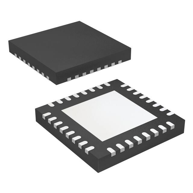


 工商网监
湘ICP备2023018690号
工商网监
湘ICP备2023018690号

