Product
Folder
Sample &
Buy
Support &
Community
Tools &
Software
Technical
Documents
LM61
SNIS121J – JUNE 1999 – REVISED NOVEMBER 2016
LM61 2.7-V, SOT-23 or TO-92 Temperature Sensor
1 Features
3 Description
•
•
The LM61 device is a precision, integrated-circuit
temperature sensor that can sense a –30°C to 100°C
temperature range while operating from a single
2.7‑V supply. The output voltage of the LM61 is
linearly proportional to temperature (10 mV/°C) and
has a DC offset of 600 mV. The offset allows reading
negative temperatures without the need for a
negative supply. The nominal output voltage of the
LM61 ranges from 300 mV to 1600 mV for a –30°C to
100°C temperature range. The LM61 is calibrated to
provide accuracies of ±2°C at room temperature and
±3°C over the full –25°C to 85°C temperature range.
1
•
•
•
•
•
•
•
•
•
•
Calibrated Linear Scale Factor of 10 mV/°C
Rated for Full Temperature Range (–30° to
100°C)
Suitable for Remote Applications
UL Recognized Component
±2°C or ±3°C Accuracy at 25°C (Maximum)
±3°C Accuracy for –25°C to 85°C (Maximum)
±4°C Accuracy for –30°C to 100°C (Maximum)
10 mV/°C Temperature Slope (Maximum)
2.7-V to 10-V Power Supply Voltage Range
125-µA Current Drain at 25°C (Maximum)
±0.8°C Nonlinearity (Maximum)
800-Ω Output Impedance (Maximum)
2 Applications
•
•
•
•
•
•
•
•
•
Cellular Phones
Computers
Power Supply Modules
Battery Management
FAX Machines
Printers
HVAC
Disk Drives
Appliances
The linear output of the LM61, 600-mV offset, and
factory calibration simplify external circuitry required
in a single supply environment where reading
negative temperatures is required. Because the
quiescent current is less than 125 µA, self-heating is
limited to a very low 0.2°C in still air. Shutdown
capability for the LM61 is intrinsic because its
inherent low power consumption allows it to be
powered directly from the output of many logic gates.
Device Information(1)
PART NUMBER
PACKAGE
LM61
BODY SIZE (NOM)
SOT-23 (3)
1.30 mm × 2.92 mm
TO-92 (3)
4.30 mm × 4.30 mm
(1) For all available packages, see the orderable addendum at
the end of the data sheet.
Key Specifications
Typical Application
VALUE
Accuracy at 25°C
±2°C or ±3°C
Accuracy for –25°C to 85°C
±3°C
Accuracy for –30°C to 100°C
±4°C
Temperature slope
10 mV/°C
Power supply voltage
2.7 V to 10 V
Current drain at 25°C
125 µA
Nonlinearity
±0.8°C
Output impedance
800 Ω
VO = (10 mV/°C × T°C) + 600 mV
1
An IMPORTANT NOTICE at the end of this data sheet addresses availability, warranty, changes, use in safety-critical applications,
intellectual property matters and other important disclaimers. PRODUCTION DATA.
�LM61
SNIS121J – JUNE 1999 – REVISED NOVEMBER 2016
www.ti.com
Table of Contents
1
2
3
4
5
6
7
Features ..................................................................
Applications ...........................................................
Description .............................................................
Revision History.....................................................
Pin Configuration and Functions .........................
Specifications.........................................................
1
1
1
2
3
3
6.1
6.2
6.3
6.4
6.5
6.6
3
3
3
4
4
5
Absolute Maximum Ratings ......................................
ESD Ratings..............................................................
Recommended Operating Conditions.......................
Thermal Information ..................................................
Electrical Characteristics...........................................
Typical Characteristics ..............................................
Detailed Description .............................................. 7
7.1
7.2
7.3
7.4
Overview ...................................................................
Functional Block Diagram .........................................
Feature Description...................................................
Device Functional Modes..........................................
7
7
7
7
8
Application and Implementation .......................... 8
8.1 Application Information.............................................. 8
8.2 Typical Applications .................................................. 8
9 Power Supply Recommendations...................... 11
10 Layout................................................................... 11
10.1 Layout Guidelines ................................................. 11
10.2 Layout Examples................................................... 11
10.3 Thermal Considerations ........................................ 12
11 Device and Documentation Support ................. 14
11.1
11.2
11.3
11.4
11.5
11.6
Related Documentation.........................................
Receiving Notification of Documentation Updates
Community Resources..........................................
Trademarks ...........................................................
Electrostatic Discharge Caution ............................
Glossary ................................................................
14
14
14
14
14
14
12 Mechanical, Packaging, and Orderable
Information ........................................................... 14
4 Revision History
NOTE: Page numbers for previous revisions may differ from page numbers in the current version.
Changes from Revision I (February 2013) to Revision J
Page
•
Added Device Information table, Device Comparison Table, Pin Configuration and Functions section, Specifications
section, ESD Ratings table, Detailed Description section, Application and Implementation section, Power Supply
Recommendations section, Layout section, Device and Documentation Support section, and Mechanical,
Packaging, and Orderable Information section ...................................................................................................................... 1
•
Added Thermal Information table ........................................................................................................................................... 4
•
Changed RθJA values for DBZ (SOT-23) From: 450°C/W To: 286.3°C/W and for LP (TO-92) From: 180°C/W To:
162.2°C/W .............................................................................................................................................................................. 4
Changes from Revision H (February 2013) to Revision I
•
2
Page
Changed layout of National Semiconductor Data Sheet to TI format .................................................................................... 1
Submit Documentation Feedback
Copyright © 1999–2016, Texas Instruments Incorporated
Product Folder Links: LM61
�LM61
www.ti.com
SNIS121J – JUNE 1999 – REVISED NOVEMBER 2016
5 Pin Configuration and Functions
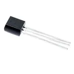
DBZ Package
3-Pin SOT-23
Top View
LP Package
3-Pin TO-92
Pin Functions
PIN
NAME
TYPE
NO.
DESCRIPTION
+VS
1
Power
Positive power supply pin.
VOUT
2
Output
Temperature sensor analog output.
GND
3
Ground
Device ground pin, connected to power supply negative terminal.
6 Specifications
6.1 Absolute Maximum Ratings
over operating free-air temperature range (unless otherwise noted) (1)
MIN
MAX
UNIT
Supply voltage
12
–0.2
V
Output voltage
(+VS + 0.6)
–0.6
V
10
mA
Output current
Input current at any pin (2)
Maximum junction temperature, TJ
Storage temperature, Tstg
(1)
(2)
–65
5
mA
125
°C
150
°C
Stresses beyond those listed under Absolute Maximum Ratings may cause permanent damage to the device. These are stress ratings
only, which do not imply functional operation of the device at these or any other conditions beyond those indicated under Recommended
Operating Conditions. Exposure to absolute-maximum-rated conditions for extended periods may affect device reliability.
When the input voltage (VI) at any pin exceeds power supplies (VI < GND or VI > VS), the current at that pin must be limited to 5 mA.
6.2 ESD Ratings
VALUE
V(ESD)
(1)
(2)
(3)
Electrostatic discharge
Human-body model (HBM), per ANSI/ESDA/JEDEC JS-001 (1) (2)
±2500
Machine Model (MM) (3)
±250
UNIT
V
JEDEC document JEP155 states that 500-V HBM allows safe manufacturing with a standard ESD control process.
The human body model is a 100-pF capacitor discharged through a 1.5-kΩ resistor into each pin.
The machine model is a 200-pF capacitor discharged directly into each pin.
6.3 Recommended Operating Conditions
+VS
Supply voltage
T
Operating temperature
MIN
MAX
2
10
LM61C
–30
100
LM61B
–25
85
Submit Documentation Feedback
Copyright © 1999–2016, Texas Instruments Incorporated
Product Folder Links: LM61
UNIT
V
°C
3
�LM61
SNIS121J – JUNE 1999 – REVISED NOVEMBER 2016
www.ti.com
6.4 Thermal Information
LM61
THERMAL METRIC (1)
DBZ (SOT-23)
LP (TO-92)
3 PINS
3 PINS
UNIT
286.3
162.2
°C/W
RθJA
Junction-to-ambient thermal resistance (2)
RθJC(top)
Junction-to-case (top) thermal resistance
96
85
°C/W
RθJB
Junction-to-board thermal resistance
57.1
—
°C/W
ψJT
Junction-to-top characterization parameter
5.3
29.2
°C/W
ψJB
Junction-to-board characterization parameter
55.8
141.4
°C/W
(1)
(2)
For more information about traditional and new thermal metrics, see the Semiconductor and IC Package Thermal Metrics application
report.
The junction-to-ambient thermal resistance is specified without a heat sink in still air.
6.5 Electrical Characteristics
+VS = 3 V (DC) (1) (2)
PARAMETER
TEST CONDITIONS
TA = 25°C
Accuracy (5)
MIN (3)
Sensor gain (average slope)
Output impedance
–2
2
LM61C
–3
3
LM61B
–3
3
LM61C
–4
–0.6
0.6
LM61C
–0.8
0.8
LM61B
9.7
10
10.3
LM61C
9.6
10
10.4
+VS = 3 V to 10 V
0.8
TA = –30°C to 85°C, +VS = 2.7 V
2.3
4
5
mV/V
+VS = 2.7 V to 3.3 V
–5.7
5.7
mV
+VS = 2.7 V to 10 V
(8)
kΩ
0.7
TA = 25°C
Temperature coefficient of quiescent current
(7)
mV/°C
–0.7
Change of quiescent current
(6)
°C
+VS = 3 V to 10 V
+VS = 2.7 V to 10 V
(1)
(2)
(3)
(4)
(5)
°C
mV
LM61B
Quiescent current
Long term stability (8)
UNIT
4
600
TA = 85°C to 100°C, +VS = 2.7 V
Line regulation (7)
MAX (3)
LM61B
Output voltage at 0°C
Nonlinearity (6)
TYP (4)
TJ = TMAX = 100°C, for 1000 hours
82
125
155
µA
±5
µA
0.2
µA/°C
±0.2
°C
Limits are specified to TI's AOQL (Average Outgoing Quality Level).
Typical limits represent most likely parametric norm.
Maximum and minimum limits apply for TA = TJ = TMIN to TMAX.
Typical limits apply for TA = TJ = 25°C.
Accuracy is defined as the error between the output voltage and 10 mV/°C multiplied by the device's case temperature plus 600 mV, at
specified conditions of voltage, current, and temperature (expressed in °C).
Nonlinearity is defined as the deviation of the output-voltage-versus-temperature curve from the best-fit straight line, over the device's
rated temperature range.
Regulation is measured at constant junction temperature, using pulse testing with a low duty cycle. Changes in output due to heating
effects can be computed by multiplying the internal dissipation by the thermal resistance.
For best long-term stability, any precision circuit gives best results if the unit is aged at a warm temperature, or temperature cycled for at
least 46 hours before long-term life test begins. This is especially true when a small (Surface-Mount) part is wave-soldered; allow time
for stress relaxation to occur. The majority of the drift occurs in the first 1000 hours at elevated temperatures. The drift after 1000 hours
does not continue at the first 1000-hour rate.
Submit Documentation Feedback
Copyright © 1999–2016, Texas Instruments Incorporated
Product Folder Links: LM61
�LM61
www.ti.com
SNIS121J – JUNE 1999 – REVISED NOVEMBER 2016
6.6 Typical Characteristics
The LM61 in the SOT-23 package mounted to a printed-circuit board as shown in Figure 18 was used to generate the
following thermal curves.
Figure 1. Junction-to-Ambient Thermal Resistance
Figure 2. Thermal Time Constant
Figure 3. Thermal Response in Still Air with Heat Sink
Figure 4. Thermal Response in Stirred Oil Bath
with Heat Sink
Figure 5. Thermal Response in Still Air without Heat Sink
Figure 6. Quiescent Current vs Temperature
Submit Documentation Feedback
Copyright © 1999–2016, Texas Instruments Incorporated
Product Folder Links: LM61
5
�LM61
SNIS121J – JUNE 1999 – REVISED NOVEMBER 2016
www.ti.com
Typical Characteristics (continued)
The LM61 in the SOT-23 package mounted to a printed-circuit board as shown in Figure 18 was used to generate the
following thermal curves.
Figure 7. Accuracy vs Temperature
Figure 8. Noise Voltage
+VS
2 V/Div
0V
0.2 V/Div
VO
0V
5 µs/Div
Figure 9. Supply Voltage vs Supply Current
Figure 10. Start-Up Response
6
Submit Documentation Feedback
Copyright © 1999–2016, Texas Instruments Incorporated
Product Folder Links: LM61
�LM61
www.ti.com
SNIS121J – JUNE 1999 – REVISED NOVEMBER 2016
7 Detailed Description
7.1 Overview
The LM61 is a precision integrated-circuit temperature sensor that can sense a –30°C to 100°C temperature
range using a single positive supply. The output voltage of the LM61 has a positive temperature slope of
10 mV/°C. A 600-mV offset is included, enabling negative temperature sensing when biased by a single supply.
The temperature-sensing element is comprised of a delta-VBE architecture. The temperature-sensing element is
then buffered by an amplifier and provided to the VOUT pin. The amplifier has a simple class A output stage as
shown in Functional Block Diagram.
7.2 Functional Block Diagram
7.3 Feature Description
7.3.1 LM61 Transfer Function
The LM61 follows a simple linear transfer function to achieve the accuracy as listed in Electrical Characteristics.
Use Equation 1 to calculate the value of VO.
VO = 10 mV/°C × T°C + 600 mV
where
•
•
T is the temperature in °C
VO is the LM61 output voltage
(1)
7.4 Device Functional Modes
The only functional mode of the LM61 device is an analog output directly proportional to temperature.
Submit Documentation Feedback
Copyright © 1999–2016, Texas Instruments Incorporated
Product Folder Links: LM61
7
�LM61
SNIS121J – JUNE 1999 – REVISED NOVEMBER 2016
www.ti.com
8 Application and Implementation
NOTE
Information in the following applications sections is not part of the TI component
specification, and TI does not warrant its accuracy or completeness. TI’s customers are
responsible for determining suitability of components for their purposes. Customers should
validate and test their design implementation to confirm system functionality.
8.1 Application Information
The LM61 has a wide supply range and a 10-mV/°C output slope with a 600-mV DC. Therefore, it can be easily
applied in many temperature-sensing applications where a single supply is required for positive and negative
temperatures.
8.2 Typical Applications
8.2.1 Typical Temperature Sensing Circuit
VO = 10 mV/°C × T°C + 600 mV
Figure 11. Typical Temperature Sensing Circuit Diagram
8.2.1.1 Design Requirements
For this design example, use the parameters listed in Table 1 as the input parameters.
Table 1. Design Parameters
8
PARAMETER
VALUE
Power supply voltage
2.7 V to 3.3 V
Accuracy at 25°C
±2°C (maximum)
Accuracy over –25°C to 85°C
±3°C (maximum)
Temperature slope
10 mV/°C
Submit Documentation Feedback
Copyright © 1999–2016, Texas Instruments Incorporated
Product Folder Links: LM61
�LM61
www.ti.com
SNIS121J – JUNE 1999 – REVISED NOVEMBER 2016
8.2.1.2 Detailed Design Procedure
The LM61 is a simple temperature sensor that provides an analog output. Therefore, design requirements related
to layout outweigh other requirements in importance. See Layout for more information.
8.2.1.2.1 Capacitive Loads
The LM61 handles capacitive loading well. Without any special precautions, the LM61 can drive any capacitive
load as shown in Figure 12. Over the specified temperature range the LM61 has a maximum output impedance
of 5 kΩ. In an extremely noisy environment it may be necessary to add some filtering to minimize noise pickup. It
is recommended that 0.1-µF capacitor be added between +VS and GND to bypass the power-supply voltage, as
shown in Figure 13. In a noisy environment it may be necessary to add a capacitor from VOUT to ground. A 1-µF
output capacitor with the 5-kΩ maximum output impedance forms a 32-Hz lowpass filter. Because the thermal
time constant of the LM61 is much slower than the 5-ms time constant formed by the RC, the overall response
time of the LM61 is not significantly affected. For much larger capacitors this additional time lag increases the
overall response time of the LM61.
Figure 12. LM61 No Decoupling Required for Capacitive Load
Figure 13. LM61 with Filter for Noisy Environments
Submit Documentation Feedback
Copyright © 1999–2016, Texas Instruments Incorporated
Product Folder Links: LM61
9
�LM61
SNIS121J – JUNE 1999 – REVISED NOVEMBER 2016
www.ti.com
8.2.1.3 Application Curve
Figure 14. Accuracy vs Temperature
8.2.2 Other Application Circuits
Figure 15 shows an application circuit example using the LM61 device. Customers must fully validate and test
any circuit before implementing a design based on an example in this section. Unless otherwise noted, the
design procedures in Typical Temperature Sensing Circuit are applicable.
V+
VTEMP
R3
VT1
R4
VT2
LM4040
V+
VT
R1
4.1V
U3
0.1 PF
LM61
R2
(Low = overtemp alarm)
+
U1
-
VOUT
VOUT
LM7211
VTemp
U2
VT1 =
(4.1)R2
R2 + R1||R3
VT2 =
(4.1)R2||R3
R1 + R2||R3
Copyright © 2016, Texas Instruments Incorporated
Figure 15. Centigrade Thermostat
Figure 16. Conserving Power Dissipation with Shutdown
10
Submit Documentation Feedback
Copyright © 1999–2016, Texas Instruments Incorporated
Product Folder Links: LM61
�LM61
www.ti.com
SNIS121J – JUNE 1999 – REVISED NOVEMBER 2016
9 Power Supply Recommendations
In an extremely noisy environment, it may be necessary to add filtering to minimize noise pickup. TI recommends
a 0.1-µF capacitor be added between +VS to GND to bypass the power-supply voltage, as shown in Figure 13.
10 Layout
10.1 Layout Guidelines
10.1.1 Mounting
The LM61 can be applied easily in the same way as other integrated-circuit temperature sensors. It can be glued
or cemented to a surface. The temperature that the LM61 senses is within about 0.2°C of the surface
temperature that LM61's leads are attached to.
This presumes that the ambient air temperature is almost the same as the surface temperature; if the air
temperature is much higher or lower than the surface temperature, the actual temperature measured would be at
an intermediate temperature between the surface temperature and the air temperatures.
To ensure good thermal conductivity the backside of the LM61 die is directly attached to the GND pin. The lands
and traces to the LM61 are part of the printed-circuit board, which is the object whose temperature is being
measured.
Alternatively, the LM61 can be mounted inside a sealed-end metal tube, and can then be dipped into a bath or
screwed into a threaded hole in a tank. As with any IC, the LM61 and accompanying wiring and circuits must be
kept insulated and dry, to avoid leakage and corrosion. This is especially true if the circuit may operate at cold
temperatures where condensation can occur. Printed-circuit coatings and varnishes such as Humiseal and epoxy
paints or dips are often used to ensure that moisture cannot corrode the device or connections.
10.2 Layout Examples
Figure 17. Recommended Solder Pads for SOT-23 Package
Submit Documentation Feedback
Copyright © 1999–2016, Texas Instruments Incorporated
Product Folder Links: LM61
11
�LM61
SNIS121J – JUNE 1999 – REVISED NOVEMBER 2016
www.ti.com
Layout Examples (continued)
A.
1/2 in.2 printed-circuit board with 2 oz copper foil or similar.
Figure 18. Printed-Circuit Board Used for Heat Sink to Generate All Curves
+VS
1
3
VO
GND
2
Via to ground plane
Via to power plane
Figure 19. PCB Layout
10.3 Thermal Considerations
The junction-to-ambient thermal resistance is the parameter used to calculate the rise of a device junction
temperature due to its power dissipation. For the LM61, Equation 2 is used to calculate the rise in the die
temperature.
TJ = TA + RθJA × ((+VS × IQ) + (+VS – VO) × IL)
where
•
•
IQ is the quiescent current
ILis the load current on the output
(2)
Table 2 summarizes the rise in die temperature of the LM61 without any loading with a 3.3-V supply, and the
thermal resistance for different conditions.
12
Submit Documentation Feedback
Copyright © 1999–2016, Texas Instruments Incorporated
Product Folder Links: LM61
�LM61
www.ti.com
SNIS121J – JUNE 1999 – REVISED NOVEMBER 2016
Table 2. Temperature Rise of LM61 Due to Self-Heating and Thermal Resistance
(RθJA)
Still air
No heat sink (1)
Moving air
SOT-23
Small heat fin (2)
No heat sink (1)
TO-92
Small heat fin (3)
(1)
(2)
(3)
RθJA (°C/W)
TJ – TA (°C)
450
0.26
—
—
Still air
260
0.13
Moving air
180
0.09
Still air
180
0.09
Moving air
90
0.05
Still air
140
0.07
Moving air
70
0.03
Part soldered to 30 gauge wire.
Heat sink used is 1/2 in.2 printed -circuit board with 2-oz foil with part attached as shown in Figure 18.
Part glued and leads soldered to 1 in.2 of 1/16 in. printed circuit board with 2-oz foil or similar.
Table 3. Temperature and Typical VO Values
TEMPERATURE
VO(TYPICAL)
100°C
1600 mV
85°C
1450 mV
25°C
850 mV
0°C
600 mV
–25°C
350 mV
–30°C
300 mV
Submit Documentation Feedback
Copyright © 1999–2016, Texas Instruments Incorporated
Product Folder Links: LM61
13
�LM61
SNIS121J – JUNE 1999 – REVISED NOVEMBER 2016
www.ti.com
11 Device and Documentation Support
11.1 Related Documentation
For related documentation see the following:
• TO-92 Packing Options / Ordering Instructions (SNOA072)
• Tiny Temperature Sensors for Remote Systems (SNIA009)
11.2 Receiving Notification of Documentation Updates
To receive notification of documentation updates, navigate to the device product folder on ti.com. In the upper
right corner, click on Alert me to register and receive a weekly digest of any product information that has
changed. For change details, review the revision history included in any revised document.
11.3 Community Resources
The following links connect to TI community resources. Linked contents are provided "AS IS" by the respective
contributors. They do not constitute TI specifications and do not necessarily reflect TI's views; see TI's Terms of
Use.
TI E2E™ Online Community TI's Engineer-to-Engineer (E2E) Community. Created to foster collaboration
among engineers. At e2e.ti.com, you can ask questions, share knowledge, explore ideas and help
solve problems with fellow engineers.
Design Support TI's Design Support Quickly find helpful E2E forums along with design support tools and
contact information for technical support.
11.4 Trademarks
E2E is a trademark of Texas Instruments.
All other trademarks are the property of their respective owners.
11.5 Electrostatic Discharge Caution
This integrated circuit can be damaged by ESD. Texas Instruments recommends that all integrated circuits be handled with
appropriate precautions. Failure to observe proper handling and installation procedures can cause damage.
ESD damage can range from subtle performance degradation to complete device failure. Precision integrated circuits may be more
susceptible to damage because very small parametric changes could cause the device not to meet its published specifications.
11.6 Glossary
SLYZ022 — TI Glossary.
This glossary lists and explains terms, acronyms, and definitions.
12 Mechanical, Packaging, and Orderable Information
The following pages include mechanical, packaging, and orderable information. This information is the most
current data available for the designated devices. This data is subject to change without notice and revision of
this document. For browser-based versions of this data sheet, refer to the left-hand navigation.
14
Submit Documentation Feedback
Copyright © 1999–2016, Texas Instruments Incorporated
Product Folder Links: LM61
�PACKAGE OPTION ADDENDUM
www.ti.com
30-Sep-2021
PACKAGING INFORMATION
Orderable Device
Status
(1)
Package Type Package Pins Package
Drawing
Qty
Eco Plan
(2)
Lead finish/
Ball material
MSL Peak Temp
Op Temp (°C)
Device Marking
(3)
(4/5)
(6)
LM61BIM3
NRND
SOT-23
DBZ
3
1000
Non-RoHS
& Green
Call TI
Level-1-260C-UNLIM
-25 to 85
T1B
LM61BIM3/NOPB
ACTIVE
SOT-23
DBZ
3
1000
RoHS & Green
SN
Level-1-260C-UNLIM
-25 to 85
T1B
LM61BIM3X/NOPB
ACTIVE
SOT-23
DBZ
3
3000
RoHS & Green
SN
Level-1-260C-UNLIM
-25 to 85
T1B
LM61BIZ/LFT3
ACTIVE
TO-92
LP
3
2000
RoHS & Green
SN
N / A for Pkg Type
LM61BIZ/NOPB
ACTIVE
TO-92
LP
3
1800
RoHS & Green
SN
N / A for Pkg Type
-25 to 85
LM61
BIZ
LM61CIM3
NRND
SOT-23
DBZ
3
1000
Non-RoHS
& Green
Call TI
Level-1-260C-UNLIM
-30 to 100
T1C
LM61CIM3/NOPB
ACTIVE
SOT-23
DBZ
3
1000
RoHS & Green
SN
Level-1-260C-UNLIM
-30 to 100
T1C
LM61CIM3X/NOPB
ACTIVE
SOT-23
DBZ
3
3000
RoHS & Green
SN
Level-1-260C-UNLIM
-30 to 100
T1C
LM61CIZ/LFT2
ACTIVE
TO-92
LP
3
2000
RoHS & Green
SN
N / A for Pkg Type
LM61CIZ/NOPB
ACTIVE
TO-92
LP
3
1800
RoHS & Green
SN
N / A for Pkg Type
LM61
BIZ
LM61
CIZ
-30 to 100
LM61
CIZ
(1)
The marketing status values are defined as follows:
ACTIVE: Product device recommended for new designs.
LIFEBUY: TI has announced that the device will be discontinued, and a lifetime-buy period is in effect.
NRND: Not recommended for new designs. Device is in production to support existing customers, but TI does not recommend using this part in a new design.
PREVIEW: Device has been announced but is not in production. Samples may or may not be available.
OBSOLETE: TI has discontinued the production of the device.
(2)
RoHS: TI defines "RoHS" to mean semiconductor products that are compliant with the current EU RoHS requirements for all 10 RoHS substances, including the requirement that RoHS substance
do not exceed 0.1% by weight in homogeneous materials. Where designed to be soldered at high temperatures, "RoHS" products are suitable for use in specified lead-free processes. TI may
reference these types of products as "Pb-Free".
RoHS Exempt: TI defines "RoHS Exempt" to mean products that contain lead but are compliant with EU RoHS pursuant to a specific EU RoHS exemption.
Green: TI defines "Green" to mean the content of Chlorine (Cl) and Bromine (Br) based flame retardants meet JS709B low halogen requirements of