LM74500-Q1
LM74500-Q1
SNOSDB7 – DECEMBER
2020
SNOSDB7 – DECEMBER 2020
www.ti.com
LM74500-Q1 Reverse Polarity Protection Controller
1 Features
3 Description
•
The LM74500-Q1 is an automotive AEC Q100
qualified controller which operates in conjunction with
an external N-channel MOSFET as a low loss reverse
polarity protection solution. The wide supply input
range of 3.2 V to 65 V allows control of many popular
DC bus voltages such as 12-V, 24-V and 48-V
automotive battery systems. The 3.2-V input voltage
support is particularly well suited for severe cold crank
requirements in automotive systems. The device can
withstand and protect the loads from negative supply
voltages down to –65 V. The LM74500-Q1 does not
have reverse current blocking and is suitable for input
reverse poalrity protection of loads that can potentially
deliver energy back to the input supply such as
automotive body control module motor loads.
•
•
•
•
•
•
•
•
AEC-Q100 qualified with the following results
– Device temperature grade 1:
–40°C to +125°C ambient operating
temperature range
– Device HBM ESD classification level 2
– Device CDM ESD classification level C4B
3.2-V to 65-V input range (3.9-V start up)
–65-V input reverse voltage rating
Charge pump for external N-Channel MOSFET
Enable pin feature
1-µA shutdown current (EN=Low)
80-µA typical operating quiescent current
(EN=High)
Meets automotive ISO7637 pulse 1 transient
requirements with additional TVS Diode
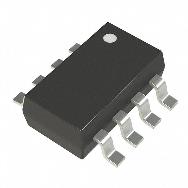
Available in 8-pin SOT-23 package 2.90 mm ×
1.60 mm
2 Applications
•
•
•
•
Body electronics and lighting
Automotive infotainment systems - digital cluster,
head unit
Automotive USB Hubs
Industrial factory automation - PLC
The LM74500-Q1 controller provides a charge pump
gate drive for an external N-channel MOSFET. The
high voltage rating of LM74500-Q1 helps to simplify
the system designs for automotive ISO7637
protection. With the enable pin low, the controller is off
and draws approximately 1 µA of current thus offering
low system current when put into sleep mode.
Device Information (1)
PART NUMBER
LM74500-Q1
(1)
VBAT
PACKAGE
SOT-23 (8)
BODY SIZE (NOM)
2.90 mm × 1.60 mm
For all available packages, see the orderable addendum at
the end of the data sheet.
VOUT
Voltage
Regulator
SOURCE
GATE
VCAP
LM74500-Q1
EN
ON OFF
GND
LM74500-Q1 Typical Application Schematic
LM74500-Q1 Startup with –12-V Supply
An©IMPORTANT
NOTICEIncorporated
at the end of this data sheet addresses availability, warranty, changes, use in
safety-critical
applications,
Copyright
2020 Texas Instruments
Submit
Document
Feedback
intellectual property matters and other important disclaimers. PRODUCTION DATA.
Product Folder Links: LM74500-Q1
1
�LM74500-Q1
www.ti.com
SNOSDB7 – DECEMBER 2020
Table of Contents
1 Features............................................................................1
2 Applications..................................................................... 1
3 Description.......................................................................1
4 Revision History.............................................................. 2
5 Pin Configuration and Functions...................................3
6 Specifications.................................................................. 4
6.1 Absolute Maximum Ratings ....................................... 4
6.2 ESD Ratings .............................................................. 4
6.3 Recommended Operating Conditions ........................4
6.4 Thermal Information ...................................................4
6.5 Electrical Characteristics ............................................5
6.6 Switching Characteristics ...........................................6
7 Typical Characteristics................................................... 7
8 Detailed Description........................................................9
8.1 Overview..................................................................... 9
8.2 Functional Block Diagram........................................... 9
8.3 Feature Description.....................................................9
8.4 Device Functional Modes..........................................11
9 Application and Implementation.................................. 12
9.1 Reverse Battery Protection for Automotive Body
Control Module Applications........................................12
9.2 Reverse Polarity Protection...................................... 14
9.3 Application Information............................................. 16
10 Power Supply Recommendations..............................20
11 Layout........................................................................... 20
11.1 Layout Guidelines................................................... 20
11.2 Layout Example...................................................... 20
12 Device and Documentation Support..........................21
12.1 Receiving Notification of Documentation Updates..21
12.2 Support Resources................................................. 21
12.3 Trademarks............................................................. 21
12.4 Electrostatic Discharge Caution..............................21
12.5 Glossary..................................................................21
13 Mechanical, Packaging, and Orderable
Information.................................................................... 22
4 Revision History
NOTE: Page numbers for previous revisions may differ from page numbers in the current version.
2
DATE
REVISION
NOTES
December 2020
*
Initial release.
Submit Document Feedback
Copyright © 2020 Texas Instruments Incorporated
Product Folder Links: LM74500-Q1
�LM74500-Q1
www.ti.com
SNOSDB7 – DECEMBER 2020
5 Pin Configuration and Functions
EN
1
8
N.C
GND
2
7
N.C
N.C
3
6
GATE
VCAP
4
5
SOURCE
Figure 5-1. DDF Package 8-Pin SOT-23 LM74500-Q1 Top View
Table 5-1. LM74500-Q1 Pin Functions
PIN
NO.
NAME
I/O(1)
DESCRIPTION
1
EN
I
Enable pin. Can be connected to SOURCE for always ON operation
2
GND
G
Ground pin
3
N.C
-
No connection
4
VCAP
O
Charge pump output. Connect to external charge pump capacitor
5
SOURCE
I
Input supply pin to the controller. Connect to the source of the external N-channel MOSFET
6
GATE
O
Gate drive output. Connect to gate of the external N-channel MOSFET
7
N.C
-
No connection
8
N.C
-
No connection
(1)
I = Input, O = Output, G = GND
Submit Document Feedback
Copyright © 2020 Texas Instruments Incorporated
Product Folder Links: LM74500-Q1
3
�LM74500-Q1
www.ti.com
SNOSDB7 – DECEMBER 2020
6 Specifications
6.1 Absolute Maximum Ratings
over operating free-air temperature range (unless otherwise noted)(1)
MIN
Input Pins
Output Pins
MAX
UNIT
SOURCE to GND
–65
65
V
EN to GND, V(SOURCE) > 0 V
–0.3
65
V
EN to GND, V(SOURCE) ≤ 0 V
V(SOURCE)
(65 + V(SOURCE))
V
GATE to SOURCE
–0.3
15
V
VCAP to SOURCE
–0.3
15
V
Operating junction temperature(2)
–40
150
°C
Storage temperature, Tstg
–40
150
°C
(1)
(2)
Stresses beyond those listed under Absolute Maximum Ratings may cause permanent damage to the device. These are stress ratings
only, which do not imply functional operation of the device at these or any other conditions beyond those indicated under
Recommended Operating Conditions. Exposure to absolute-maximum-rated conditions for extended periods may affect device
reliability.
High junction temperatures degrade operating lifetimes. Operating lifetime is de-rated for junction temperatures greater than 125°C.
6.2 ESD Ratings
VALUE
Human body model (HBM), per AEC Q100-002(1)
V(ESD)
(1)
Electrostatic discharge
Charged device model (CDM),
per AEC Q100-011
UNIT
±2000
Corner pins (EN, VCAP,
SOURCE, NC)
±750
Other pins
±500
V
JEDEC document JEP155 states that 500-V HBM allows safe manufacturing with a standard ESD control process.
6.3 Recommended Operating Conditions
over operating free-air temperature range (unless otherwise noted)(1)
MIN
Input Pins
External
capacitance
NOM
MAX
SOURCE to GND
–60
60
EN to GND
–60
60
UNIT
V
SOURCE
22
nF
VCAP to SOURCE
0.1
µF
External
MOSFET max
VGS rating
GATE to SOURCE
15
V
TJ
Operating junction temperature range(2)
(1)
(2)
–40
150
°C
Recommended Operating Conditions are conditions under which the device is intended to be functional. For specifications and test
conditions, see electrical characteristics
High junction temperatures degrade operating lifetimes. Operating lifetime is de-rated for junction temperatures greater than 125°C.
6.4 Thermal Information
LM74500-Q1
THERMAL METRIC(1)
DDF (SOT)
UNIT
8 PINS
4
RθJA
Junction-to-ambient thermal resistance
133.8
°C/W
RθJC(top)
Junction-to-case (top) thermal resistance
72.6
°C/W
RθJB
Junction-to-board thermal resistance
54.5
°C/W
ΨJT
Junction-to-top characterization parameter
4.6
°C/W
Submit Document Feedback
Copyright © 2020 Texas Instruments Incorporated
Product Folder Links: LM74500-Q1
�LM74500-Q1
www.ti.com
SNOSDB7 – DECEMBER 2020
6.4 Thermal Information (continued)
LM74500-Q1
THERMAL
METRIC(1)
DDF (SOT)
UNIT
8 PINS
ΨJB
(1)
Junction-to-board characterization parameter
54.2
°C/W
For more information about traditional and new thermal metrics, see the Semiconductor and IC Package Thermal Metrics application
report, SPRA953.
6.5 Electrical Characteristics
TJ = –40°C to +125°C; typical values at TJ = 25°C, V(SOURCE) = 12 V, C(VCAP) = 0.1 µF, V(EN) = 3.3 V, over operating free-air
temperature range (unless otherwise noted)
PARAMETER
TEST CONDITIONS
MIN
TYP
MAX
UNIT
VSOURCE SUPPLY VOLTAGE
V(SOURCE)
V(SOURCE POR)
Operating input voltage
4
60
VSOURCE POR Rising threshold
VSOURCE POR Falling threshold
2.2
V(SOURCE POR(Hys)) VSOURCE POR Hysteresis
I(SHDN)
Shutdown Supply Current
I(Q)
Operating Quiescent Current
2.8
0.44
V(EN) = 0 V
V
3.9
V
3.1
V
0.67
V
0.9
1.5
µA
80
130
µA
ENABLE INPUT
V(EN_IL)
Enable input low threshold
0.5
0.9
1.22
V(EN_IH)
Enable input high threshold
1.06
2
2.6
V(EN_Hys)
Enable Hysteresis
I(EN)
Enable sink current
V(EN) = 12 V
Peak source current
V(GATE) – V(SOURCE) = 5 V
Peak sink current
EN= High to Low
V(GATE) – V(SOURCE) = 5 V
discharge switch RDSON
EN = High to Low
V(GATE) – V(SOURCE) = 100 mV
0.4
Charge Pump source current (Charge
pump on)
V(VCAP) – V(SOURCE) = 7 V
162
Charge Pump sink current (Charge
pump off)
V(VCAP) – V(SOURCE) = 14 V
V(VCAP) –
V(SOURCE)
Charge pump voltage at V(SOURCE) =
3.2 V
I(VCAP) ≤ 30 µA
V(VCAP) –
V(SOURCE)
Charge pump turn on voltage
10.3
11.6
13
V
V(VCAP) –
V(SOURCE)
Charge pump turn off voltage
11
12.4
13.9
V
V(VCAP) –
V(SOURCE)
Charge Pump Enable comparator
Hysteresis
0.4
0.8
1.2
V
V(VCAP UVLO)
V(VCAP) – V(SOURCE) UV release at
rising edge
5.7
6.5
7.5
V
V(VCAP UVLO)
V(VCAP) – V(SOURCE) UV threshold at
falling edge
5.05
5.4
6.2
V
0.52
3
V
1.35
V
5
µA
GATE DRIVE
I(GATE)
RDSON
3
11
mA
2370
mA
2
Ω
300
600
µA
5
10
µA
CHARGE PUMP
I(VCAP)
8
V
Submit Document Feedback
Copyright © 2020 Texas Instruments Incorporated
Product Folder Links: LM74500-Q1
5
�LM74500-Q1
www.ti.com
SNOSDB7 – DECEMBER 2020
6.6 Switching Characteristics
TJ = –40°C to +125°C; typical values at TJ = 25°C, V(SOURCE) = 12 V, CIN = C(VCAP) = COUT = 0.1 µF, V(EN) = 3.3 V, over
operating free-air temperature range (unless otherwise noted)
PARAMETER
ENTDLY
6
TEST CONDITIONS
Enable (low to high) to Gate Turn On
delay
V(VCAP) > V(VCAP UVLOR)
Submit Document Feedback
MIN
TYP
MAX
75
110
UNIT
µs
Copyright © 2020 Texas Instruments Incorporated
Product Folder Links: LM74500-Q1
�LM74500-Q1
www.ti.com
SNOSDB7 – DECEMBER 2020
7 Typical Characteristics
3.6
700
3.3
630
560
2.7
Quiescent Current (PA)
Shutdown Current (PA)
3
2.4
2.1
1.8
1.5
-40
25
85
125
150
1.2
0.9
0.6
0.3
420
350
280
210
70
0
0
5
10 15 20 25 30 35 40 45 50 55 60 65
VSOURCE (V)
7450
Figure 7-1. Shutdown Supply Current vs Supply Voltage
0
325
500
300
450
275
250
225
200
175
-40
25
85
125
150
150
125
100
5
10 15 20 25 30 35 40 45 50 55 60 65
VSOURCE (V)
7450
Figure 7-2. Operating Quiescent Current vs Supply Voltage
Charge Pump Current (PA)
Charge Pump Current (PA)
490
140
0
-40
25
85
125
150
400
350
300
250
200
150
75
100
3
4
5
6
7
8
VSOURCE (V)
9
10
11
12
0
2
4
CPI_
Figure 7-3. Charge Pump Current vs Supply Voltage at VCAP = 6
V
6
VCAP (V)
8
10
12
VCAP
Figure 7-4. Charge Pump V-I Characteristics at VSOURCE > = 12 V
2.5
220
-40
25
85
125
150
180
160
Enable Rising Threshold (V)
Enable Falling Threshold (V)
2.1
Enable Threshold (V)
200
Charge Pump Current (PA)
-40
25
85
125
150
140
120
100
80
1.7
1.3
0.9
60
40
20
0
1
2
3
4
5
VCAP (V)
6
7
8
9
0.5
-40
VCAP
Figure 7-5. Charge Pump V-I Characteristics at VSOURCE = 3.2 V
0
40
80
Free-Air Temperature (qC)
120
160
EN_R
Figure 7-6. Enable Rising and Falling threshold vs Temperature
Submit Document Feedback
Copyright © 2020 Texas Instruments Incorporated
Product Folder Links: LM74500-Q1
7
�LM74500-Q1
www.ti.com
SNOSDB7 – DECEMBER 2020
7 Typical Characteristics (continued)
13.4
Charge Pump ON/OFF Threshold (V)
90
Enable to Gate Delay (Ps)
75
60
45
30
ENTDLY ON
ENTDLY OFF
15
0
-40
0
40
80
Free-Air Temperature (qC)
120
5.8
5.4
120
160
11.9
0
3.1
3.05
3
2.95
2.9
2.85
2.8
2.75
2.7
2.65
2.6
2.55
2.5
2.45
2.4
2.35
2.3
-40
40
80
Free-Air Temperature (qC)
120
160
VCAP
VSOURCE PORR
VSOURCE PORF
-20
VCAP
Figure 7-9. Charge Pump UVLO Threshold vs Temperature
8
SOURCE POR Threshold (V)
Charge Pump UVLO Threshold (V)
VCAP UVLOR
VCAP UVLOF
40
80
Free-Air Temperature (qC)
12.2
Figure 7-8. Charge Pump ON/OFF Threshold vs Temperature
6.6
0
VCAP ON
VCAP OFF
12.5
ENTD
7
5
-40
12.8
11.6
-40
160
Figure 7-7. Enable to Gate Delay vs Temperature
6.2
13.1
0
20
40
60
80 100
Free-Air Temperature (qC)
120
140
160
VANO
Figure 7-10. VSOURCE POR Threshold vs Temperature
Submit Document Feedback
Copyright © 2020 Texas Instruments Incorporated
Product Folder Links: LM74500-Q1
�LM74500-Q1
www.ti.com
SNOSDB7 – DECEMBER 2020
8 Detailed Description
8.1 Overview
The LM74500-Q1 controller has all the features necessary to implement an efficient and fast reverse polarity
protection circuit. This easy to use reverse polarity protection controller is paired with an external N-channel
MOSFET to replace other reverse polarity schemes such as a P-channel MOSFET. An internal charge pump is
used to drive the external N-Channel MOSFET to a maximum gate drive voltage of approximately 15 V. An
enable pin, EN is available to place the LM74500-Q1 in shutdown mode disabling the N-Channel MOSFET and
minimizing the quiescent current.
8.2 Functional Block Diagram
SOURCE
GATE
VCAP
Bias Rails
VSOURCE
ENGATE
VSOURCE
VSOURCE
VCAP_UV
GATE DRIVER
ENABLE
LOGIC
VCAP_UV
VSOURCE
VSOURCE
Charge
Pump
Charge Pump
Enable Logic
VCAP
ENABLE LOGIC
VCAP_UV
REVERSE
PROTECTION
LOGIC
VCAP
VCAP
EN
GND
8.3 Feature Description
8.3.1 Input Voltage
The SOURCE pin is used to power the LM74500-Q1's internal circuitry, typically drawing 80 µA when enabled
and 1 µA when disabled. If the SOURCE pin voltage is greater than the POR Rising threshold, then LM74500Q1 operates in either shutdown mode or conduction mode in accordance with the EN pin voltage. The voltage
from SOURCE to GND is designed to vary from 65 V to –65 V, allowing the LM74500-Q1 to withstand negative
voltage transients.
8.3.2 Charge Pump
The charge pump supplies the voltage necessary to drive the external N-channel MOSFET. An external charge
pump capacitor is placed between VCAP and SOURCE pin to provide energy to turn on the external MOSFET.
In order for the charge pump to supply current to the external capacitor the EN pin voltage must be above the
Submit Document Feedback
Copyright © 2020 Texas Instruments Incorporated
Product Folder Links: LM74500-Q1
9
�LM74500-Q1
www.ti.com
SNOSDB7 – DECEMBER 2020
specified input high threshold, V(EN_IH). When enabled the charge pump sources a charging current of 300 µA
typically. If EN pins is pulled low, then the charge pump remains disabled. To ensure that the external MOSFET
can be driven above its specified threshold voltage, the VCAP to SOURCE voltage must be above the
undervoltage lockout threshold, typically 6.5 V, before the internal gate driver is enabled. Use Equation 1 to
calculate the initial gate driver enable delay.
T DRV _ EN
75Ps C(VCAP) x
V(VCAP _ UVLOR)
300PA
(1)
where
•
•
C(VCAP) is the charge pump capacitance connected across SOURCE and VCAP pins
V(VCAP_UVLOR) = 6.5 V (typical)
To remove any chatter on the gate drive approximately 800 mV of hysteresis is added to the VCAP undervoltage
lockout. The charge pump remains enabled until the VCAP to SOURCE voltage reaches 12.4 V, typically, at
which point the charge pump is disabled decreasing the current draw on the SOURCE pin. The charge pump
remains disabled until the VCAP to SOURCE voltage is below to 11.6 V typically at which point the charge pump
is enabled. The voltage between VCAP and SOURCE continue to charge and discharge between 11.6 V and
12.4 V as shown in Figure 8-1. By enabling and disabling the charge pump, the operating quiescent current of
the LM74500-Q1 is reduced. When the charge pump is disabled it sinks 5-µA typical.
TDRV_EN
TON
TOFF
VIN
VSOURCE
0V
VEN
12.4 V
11.6 V
VCAP-VSOURCE
6.5 V
V(VCAP UVLOR)
GATE DRIVER
ENABLE
Figure 8-1. Charge Pump Operation
8.3.3 Gate Driver
The gate driver is used to control the external N-Channel MOSFET by setting the appropriate GATE to SOURCE
voltage .
Before the gate driver is enabled following three conditions must be achieved:
• The EN pin voltage must be greater than the specified input high voltage.
• The VCAP to SOURCE voltage must be greater than the undervoltage lockout voltage.
• The SOURCE voltage must be greater than VSOURCE POR Rising threshold.
10
Submit Document Feedback
Copyright © 2020 Texas Instruments Incorporated
Product Folder Links: LM74500-Q1
�LM74500-Q1
www.ti.com
SNOSDB7 – DECEMBER 2020
If the above conditions are not achieved, then the GATE pin is internally connected to the SOURCE pin, assuring
that the external MOSFET is disabled. Once these conditions are achieved the gate driver operates in the
conduction mode enhancing the external MOSFET completely.
8.3.4 Enable
The LM74500-Q1 has an enable pin, EN. The enable pin allows for the gate driver to be either enabled or
disabled by an external signal. If the EN pin voltage is greater than the rising threshold, the gate driver and
charge pump operates as described in Gate Driver and Charge Pump sections. If the enable pin voltage is less
than the input low threshold, the charge pump and gate driver are disabled placing the LM74500-Q1 in shutdown
mode. The EN pin can withstand a voltage as large as 65 V and as low as –65 V. This allows for the EN pin to
be connected directly to the SOURCE pin if enable functionality is not needed. In conditions where EN is left
floating, the internal sink current of 3 uA pulls EN pin low and disables the device.
8.4 Device Functional Modes
8.4.1 Shutdown Mode
The LM74500-Q1 enters shutdown mode when the EN pin voltage is below the specified input low threshold
V(EN_IL). Both the gate driver and the charge pump are disabled in shutdown mode. During shutdown mode the
LM74500-Q1 enters low IQ operation with the SOURCE pin only sinking 1 µA. When the LM74500-Q1 is in
shutdown mode, forward current flow through the external MOSFET is not interrupted but is conducted through
the MOSFET's body diode.
8.4.2 Conduction Mode
For the LM74500-Q1 to operate in conduction mode the gate driver must be enabled as described in the Gate
Driver section. If these conditions are achieved the GATE pin is internally connected to the VCAP pin resulting in
the GATE to SOURCE voltage being approximately the same as the VCAP to SOURCE voltage. By connecting
VCAP to GATE the external MOSFET's RDS(ON) is minimized reducing the power loss of the external MOSFET
when forward currents are large.
Submit Document Feedback
Copyright © 2020 Texas Instruments Incorporated
Product Folder Links: LM74500-Q1
11
�LM74500-Q1
www.ti.com
SNOSDB7 – DECEMBER 2020
9 Application and Implementation
Note
Information in the following applications sections is not part of the TI component specification, and TI
does not warrant its accuracy or completeness. TI’s customers are responsible for determining
suitability of components for their purposes, as well as validating and testing their design
implementation to confirm system functionality.
9.1 Reverse Battery Protection for Automotive Body Control Module Applications
Reverse-battery protection activates when battery terminals are incorrectly connected during jump start, vehicle
maintenance or service because a connection error can damage the components in ECUs if they are not rated to
handle reverse polarity. An N-channel MOSFET (N-FET) based reverse polarity protection solutions are
becoming obivious choice over discrete reverse-battery protection solutions like Schottky diodes and P-channel
field-effect transistors (P-FETs) due to their better power and thermal efficiency and the comparitively smaller
space they consume on a printed circuit board. Based on the application needs, reverse polarity protection
solutions can be divided into two main categories
•
•
Applications which need both input reverse polarity protection and reverse current blocking
Applications which need only input reverse polarity protection and does not need reverse current blocking
Figure 9-1 provides an overview of these two reverse polarity protection solution categories. Typically for
applications where output loads are DC/DC converters, voltage regulator followed by MCU/processors (Logic
paths), input reverse polarity protection and reverse current blocking feature is required. For reverse polarity
protection solution of the logic path ideal diode controllers such as LM74700-Q1 is a suitable device.
12
Submit Document Feedback
Copyright © 2020 Texas Instruments Incorporated
Product Folder Links: LM74500-Q1
�LM74500-Q1
www.ti.com
SNOSDB7 – DECEMBER 2020
For the applications such as Body Control Module (BCM) load driving paths, input reverse polarity protection is
required but reverse current blocking is not a must have feature. For reverse polarity protection solution of the
BCM load driving paths, reverse polarity potection controllers such as LM74500-Q1 is a suitable device.
Load Driving Path
x
Reverse Polarity Protection: Required
x
Revere Current Blocking: Not Required
Wiper/Washer
LM74500-Q1
Relays
Horn/Alarm
VBAT
Linear
Regulator
LM74700-Q1
DC/DC
Converters
Voltage
Supervisors
Logic Path
x
Reverse Polarity Protection: Required
x
Revere Current Blocking: Required
Figure 9-1. Typical Block Diagram for Automotive BCM Reverse Battery Protection Solution
For certain applications such as body control module load driving paths where output loads are inductive in
nature such as wiper motor, door control module, it is required that reverse polarity protection device should
provide protection against incorrect input polarity. However, it should not block reverse current from loads back
to the battery. This is mainly required to avoid voltage overshoot which is caused when inductive loads are
turned off. If reverse polarity protection device blocks the reverse current then there could be voltage overshoot
caused due to inductive kick back or motor regenrative action and can damage parallel loads connected on the
output of reverse polarity protection device. For certain specific loads such as wiper motor, a voltage overshoot
is seen due to transformer effect when wiper motor speed is changed from fast speed to slow speed. LM74500Q1 is designed to provide protection against input reverse polarity for such applications where reverse current
Submit Document Feedback
Copyright © 2020 Texas Instruments Incorporated
Product Folder Links: LM74500-Q1
13
�LM74500-Q1
www.ti.com
SNOSDB7 – DECEMBER 2020
blocking is not reuiqred. Figure 9-2 shows typical application circuit of reverse polarity protection of body control
module load driving paths.
Reverse current
blocking is not
preferred
Wiper/
Washer
Q1
Door module
CIN
VBAT
Input
TVS
EN
SOURCE
VCAP
Input reverse polarity
protection is required
GATE
COUT
Relays
LM74500
Lighting
Modules
VCAP
GND
Figure 9-2. Typical Block Diagram of Reverse Battery Protection for Body Control Module Load Driving
Path
9.2 Reverse Polarity Protection
P-FET based reverse polarity protection is a very commonly used scheme in industrial and automotive
applications to achieve low insertion loss protection solution. A low loss reverse polarity protection solution can
be realised using LM74500-Q1 with an external N-FET to replace P-FET based solution. LM74500-Q1 based
reverse polarity protection solution offers better cold crank performance (low VIN operation) and smaller solution
size compared to P-FET based solution. Figure 9-3 compares the performance benefits of LM74500-Q1 +N-FET
over traditional P-FET based reverse polarity protection solution. As shown in Figure 9-3, for a given power level
LM74500-Q1+N-FET solution can be three times smaller than a similar power rated P-FET solution. Also as PFET is self biased by simply pulling it's gate pin low and thus P-FET shows poorer cold crank performance (low
VIN operation) compared to LM74500-Q1. During severe cold crank where battery voltage falls below 4 V, P-FET
series resistance increase drastically as shown in Figure 9-3. This leads to higher voltage drop across the PFET. Also with higher gate to source threshold (VT) this can sometimes lead to system reset due to turning off of
14
Submit Document Feedback
Copyright © 2020 Texas Instruments Incorporated
Product Folder Links: LM74500-Q1
�LM74500-Q1
www.ti.com
SNOSDB7 – DECEMBER 2020
the P-FET. On the other side LM74500-Q1 has excellent severe cold crank performance. LM74500-Q1 keeps
external FET completely enhanced even when input voltage falls to 3.2 V during severe cold crank operation.
Parameter
P-FET
LM74500-Q1 + N-FET
VOUT
VBATT
VOUT
VBATT
Typical Application
Diagram
CIN
COUT
TVS
TVS
CIN
D1
COUT
SOURCE
CVCAP
R1
GATE
VCAP LM74500-Q1
EN
GND
Solution Size
(Load current >6A)
12mm x 11.7mm
(140mm 2)
Low VIN / Cold-Crank
Performance
7mm x 5.3mm
(37.1mm 2)
Better cold crank performance compared to PFET
based solution. External N-FET remains fully enhanced
even if input voltage falls to 3.2V.
Figure 9-3. Performance Comparison of P-FET and LM74500-Q1 Based Reverse Polarity Protection
Solution
Submit Document Feedback
Copyright © 2020 Texas Instruments Incorporated
Product Folder Links: LM74500-Q1
15
�LM74500-Q1
www.ti.com
SNOSDB7 – DECEMBER 2020
9.3 Application Information
The LM74500-Q1 is used with N-Channel MOSFET controller in a typical reverse polarity protection application.
The schematic for the 12-V battery protection application is shown in Figure 9-4 where the LM74500-Q1 is used
to drive the MOSFET Q1 in series with a battery. The TVS is not required for the LM74500-Q1 to operate, but
they are used to clamp the positive and negative voltage surges. The output capacitor COUT is recommended to
protect the immediate output voltage collapse as a result of line disturbance.
9.3.1 Typical Application
Q1
COUT
CIN
VBAT
EN
TVS
VCAP
SOURCE
Voltage
Regulator
GATE
LM74500
VCAP
GND
Figure 9-4. Typical Application Circuit
9.3.1.1 Design Requirements
A design example, with system design parameters listed in Table 9-1 is presented.
Table 9-1. Design Parameters
DESIGN PARAMETER
EXAMPLE VALUE
Input voltage range
12-V Battery, 12-V Nominal with 3.2-V Cold Crank and 35-V Load
Dump
Output voltage
3.2 V during Cold Crank to 35-V Load Dump
Output current range
3-A Nominal, 5-A Maximum
Output capacitance
220-µF Typical Output Capacitance
Automotive EMC Compliance
ISO 7637-2 and ISO 16750-2
9.3.1.2 Detailed Design Procedure
9.3.1.2.1 Design Considerations
•
•
Input operating voltage range, including cold crank and load dump conditions
Nominal load current and maximum load current
9.3.1.2.2 MOSFET Selection
The important MOSFET electrical parameters are the maximum continuous drain current ID, the maximum drainto-source voltage VDS(MAX), the maximum source current through body diode and the drain-to-source On
resistance RDSON.
The maximum continuous drain current, ID, rating must exceed the maximum continuous load current. The
maximum drain-to-source voltage, VDS(MAX), must be high enough to withstand the highest differential voltage
seen in the application. This would include any anticipated fault conditions. It is recommended to use MOSFETs
with voltage rating up to 60-V maximum with the LM74500-Q1 because SOURCE pin maximum voltage rating is
65-V. The maximum V GS LM74500-Q1 can drive is 13 V, so a MOSFET with 15-V minimum VGS rating should be
selected. If a MOSFET with VGS rating < 15 V is selected, a zener diode can be used to clamp VGS to safe level.
16
Submit Document Feedback
Copyright © 2020 Texas Instruments Incorporated
Product Folder Links: LM74500-Q1
�LM74500-Q1
www.ti.com
SNOSDB7 – DECEMBER 2020
During startup, inrush current flows through the body diode to charge the bulk hold-up capacitors at the output.
The maximum source current through the body diode must be higher than the inrush current that can be seen in
the application.
To reduce the MOSFET conduction losses, lowest possible RDS(ON) is preferred.
Based on the design requirements, preferred MOSFET ratings are:
•
60-V VDS(MAX) and ±20-V VGS(MAX)
DMT6007LFG MOSFET from Diodes Inc. is selected to meet this 12-V reverse battery protection design
requirements and it is rated at:
•
•
60-V VDS(MAX) and ±20-V VGS(MAX)
RDS(ON) 6.5-mΩ typical and 8.5-mΩ maximum rated at 4.5-V VGS to ensure lower power dissipationa cross
the FET
Thermal resistance of the MOSFET should be considered against the expected maximum power dissipation in
the MOSFET to ensure that the junction temperature (TJ) is well controlled.
9.3.1.2.3 Charge Pump VCAP, Input and Output Capacitance
Minimum required capacitance for charge pump VCAP and input/output capacitance are:
•
•
•
VCAP: Minimum 0.1 µF is required; recommended value of VCAP (µF) ≥ 10 x CISS(MOSFET) (µF)
CIN: Typical input capacitor of 0.1 µF
COUT: Typical output capacitor 220 µF
9.3.1.3 Selection of TVS Diodes for 12-V Battery Protection Applications
TVS diodes are used in automotive systems for protection against transients. In the 12-V battery protection
application circuit shown in Figure 9-5, a bi-directional TVS diode is used to protect from positive and negative
transient voltages that occur during normal operation of the car and these transient voltage levels and pulses are
specified in ISO 7637-2 and ISO 16750-2 standards.
The two important specifications of the TVS are breakdown voltage and clamping voltage. Breakdown voltage is
the voltage at which the TVS diode goes into avalanche similar to a zener diode and is specified at a low current
value typical 1 mA and the breakdown voltage should be higher than worst case steady state voltages seen in
the system. The breakdown voltage of the TVS+ should be higher than 24-V jump start voltage and 35-V
suppressed load dump voltage and less than the maximum input voltage rating of LM74500-Q1 (65 V). The
breakdown voltage of TVS- should be higher than maximum reverse battery voltage –16 V, so that the TVS- is
not damaged due to long time exposure to reverse connected battery.
Clamping voltage is the voltage the TVS diode clamps in high current pulse situations and this voltage is much
higher than the breakdown voltage. TVS diodes are meant to clamp transient pulses and should not interfere
with steady state operation. In the case of an ISO 7637-2 pulse 1, the input voltage goes up to –150 V with a
generator impedance of 10 Ω. This translates to 15 A flowing through the TVS - and the voltage across the TVS
would be close to its clamping voltage.
Submit Document Feedback
Copyright © 2020 Texas Instruments Incorporated
Product Folder Links: LM74500-Q1
17
�LM74500-Q1
www.ti.com
SNOSDB7 – DECEMBER 2020
Q1
VBAT
CIN
0.1uF
EN
TVS
SMBJ33CA
SOURCE
VCAP
0.1uF
GATE
COUT
220uF
Voltage
Regulator
LM74500
VCAP
GND
Figure 9-5. Typical 12-V Battery Protection with Single Bi-Directional TVS
The next criterion is that the absolute minimum rating of source voltage of the LM74500-Q1 (–65 V) and the
maximum VDS rating MOSFET are not exceeded. In the design example, 60-V rated MOSFET is chosen.
SMBJ series of TVS' are rated up to 600-W peak pulse power levels. This is sufficient for ISO 7637-2 pulses and
suppressed load dump (ISO-16750-2 pulse B).
9.3.1.4 Selection of TVS Diodes and MOSFET for 24-V Battery Protection Applications
Typical 24-V battery protection application circuit shown in Figure 9-6 uses two uni-directional TVS diodes to
protect from positive and negative transient voltages.
Q1
VBAT
TVS+
SMBJ58A
CIN
0.1uF
EN
SOURCE
TVSSMBJ26A
VCAP
0.1uF
GATE
COUT
220uF
Voltage
Regulator
LM74500
VCAP
GND
Figure 9-6. Typical 24-V Battery Protection with Two Uni-Directional TVS
The breakdown voltage of the TVS+ should be higher than 48-V jump start voltage, less than the absolute
maximum ratings of source and enable pin of LM74500-Q1 (65 V) and should withstand 65-V suppressed load
dump. The breakdown voltage of TVS- should be lower than maximum reverse battery voltage –32 V, so that the
TVS- is not damaged due to long time exposure to reverse connected battery.
During ISO 7637-2 pulse 1, the input voltage goes up to –600 V with a generator impedance of 50 Ω. Single bidirectional TVS cannot be used for 24-V battery protection because breakdown voltage for TVS+ ≥ 48V,
maximum negative clamping voltage is ≤ –65 V . Two uni-directional TVS connected back-back needs to be
used at the input. For positive side TVS+, SMBJ58A with the breakdown voltage of 64.4 V (minimum), 67.8
(typical) is recommended. For the negative side TVS-, SMBJ26A with breakdown voltage close to 32 V (to
withstand maximum reverse battery voltage –32 V) and maximum clamping voltage of 42 V is recommended.
For 24-V battery protection, a 75-V rated MOSFET is recommended to be used along with SMBJ26A and
SMBJ58A connected back-back at the input.
18
Submit Document Feedback
Copyright © 2020 Texas Instruments Incorporated
Product Folder Links: LM74500-Q1
�LM74500-Q1
www.ti.com
SNOSDB7 – DECEMBER 2020
9.3.1.5 Application Curves
Figure 9-7. ISO 7637-2 Pulse 1
Time (2 ms/DIV)
Figure 9-8. Response to ISO 7637-2 Pulse 1
Time (20 ms/DIV)
Time (20ms/DIV)
Figure 9-9. Startup with 3-A Load
Figure 9-10. Startup with 5-A Load
Time (200 ms/DIV)
Figure 9-11. Startup with Input Reverse Voltage (–12 V)
Submit Document Feedback
Copyright © 2020 Texas Instruments Incorporated
Product Folder Links: LM74500-Q1
19
�LM74500-Q1
www.ti.com
SNOSDB7 – DECEMBER 2020
10 Power Supply Recommendations
The LM74500-Q1 reverse polarity protection controller is designed for the supply voltage range of 3.2 V ≤
VSOURCE ≤ 65 V. If the input supply is located more than a few inches from the device, an input ceramic bypass
capacitor higher than 22 nF is recommended. To prevent LM74500-Q1 and surrounding components from
damage under the conditions of a direct output short circuit, it is necessary to use a power supply having over
load and short circuit protection.
11 Layout
11.1 Layout Guidelines
•
•
•
•
Connect SOURCE and GATE pins of LM74500-Q1 close to the MOSFET's SOURCE and GATE pins.
The high current path of for this solution is through the MOSFET, therefore it is important to use thick traces
for source and drain of the MOSFET to minimize resistive losses.
The charge pump capacitor across VCAP and SOURCE pins must be kept away from the MOSFET to lower
the thermal effects on the capacitance value.
The Gate pin of the LM74500-Q1 must be connected to the MOSFET gate with short trace. Avoid excessively
thin and long running trace to the Gate Drive.
11.2 Layout Example
MOSFET DRAIN
Signal Via
Power Via
G
Top layer
VOUT
MOSFET SOURCE
N.C
N.C
GATE
SOURCE
8
7
6
5
VIN
4
VCAP
3
N.C
GND
EN
2
CIN
1
COUT
CVCAP
GND PLANE
Figure 11-1. Layout Example
20
Submit Document Feedback
Copyright © 2020 Texas Instruments Incorporated
Product Folder Links: LM74500-Q1
�LM74500-Q1
www.ti.com
SNOSDB7 – DECEMBER 2020
12 Device and Documentation Support
12.1 Receiving Notification of Documentation Updates
To receive notification of documentation updates, navigate to the device product folder on ti.com. Click on
Subscribe to updates to register and receive a weekly digest of any product information that has changed. For
change details, review the revision history included in any revised document.
12.2 Support Resources
TI E2E™ support forums are an engineer's go-to source for fast, verified answers and design help — straight
from the experts. Search existing answers or ask your own question to get the quick design help you need.
Linked content is provided "AS IS" by the respective contributors. They do not constitute TI specifications and do
not necessarily reflect TI's views; see TI's Terms of Use.
12.3 Trademarks
TI E2E™ is a trademark of Texas Instruments.
All trademarks are the property of their respective owners.
12.4 Electrostatic Discharge Caution
This integrated circuit can be damaged by ESD. Texas Instruments recommends that all integrated circuits be handled
with appropriate precautions. Failure to observe proper handling and installation procedures can cause damage.
ESD damage can range from subtle performance degradation to complete device failure. Precision integrated circuits may
be more susceptible to damage because very small parametric changes could cause the device not to meet its published
specifications.
12.5 Glossary
TI Glossary
This glossary lists and explains terms, acronyms, and definitions.
Submit Document Feedback
Copyright © 2020 Texas Instruments Incorporated
Product Folder Links: LM74500-Q1
21
�LM74500-Q1
www.ti.com
SNOSDB7 – DECEMBER 2020
13 Mechanical, Packaging, and Orderable Information
The following pages include mechanical, packaging, and orderable information. This information is the most
current data available for the designated devices. This data is subject to change without notice and revision of
this document. For browser-based versions of this data sheet, refer to the left-hand navigation.
22
Submit Document Feedback
Copyright © 2020 Texas Instruments Incorporated
Product Folder Links: LM74500-Q1
�PACKAGE OPTION ADDENDUM
www.ti.com
7-Feb-2021
PACKAGING INFORMATION
Orderable Device
Status
(1)
Package Type Package Pins Package
Drawing
Qty
Eco Plan
(2)
Lead finish/
Ball material
MSL Peak Temp
Op Temp (°C)
Device Marking
(3)
(4/5)
(6)
LM74500QDDFRQ1
ACTIVE
SOT-23-THIN
DDF
8
3000
RoHS & Green
NIPDAU
Level-1-260C-UNLIM
-40 to 125
745F
(1)
The marketing status values are defined as follows:
ACTIVE: Product device recommended for new designs.
LIFEBUY: TI has announced that the device will be discontinued, and a lifetime-buy period is in effect.
NRND: Not recommended for new designs. Device is in production to support existing customers, but TI does not recommend using this part in a new design.
PREVIEW: Device has been announced but is not in production. Samples may or may not be available.
OBSOLETE: TI has discontinued the production of the device.
(2)
RoHS: TI defines "RoHS" to mean semiconductor products that are compliant with the current EU RoHS requirements for all 10 RoHS substances, including the requirement that RoHS substance
do not exceed 0.1% by weight in homogeneous materials. Where designed to be soldered at high temperatures, "RoHS" products are suitable for use in specified lead-free processes. TI may
reference these types of products as "Pb-Free".
RoHS Exempt: TI defines "RoHS Exempt" to mean products that contain lead but are compliant with EU RoHS pursuant to a specific EU RoHS exemption.
Green: TI defines "Green" to mean the content of Chlorine (Cl) and Bromine (Br) based flame retardants meet JS709B low halogen requirements of


 工商网监
湘ICP备2023018690号
工商网监
湘ICP备2023018690号

