LMK00338
ZHCSCZ6C – DECEMBER 2013 – REVISED JULY 2021
LMK00338 8 路输出 PCIe 第 1 代/第 2 代/第 3 代/第 4 代/第 5 代时钟缓冲器和电
平转换器
1 特性
3 说明
• 3:1 输入多路复用器
– 两个通用输入运行频率高达 400MHz,且接受
LVPECL、LVDS、CML、SSTL、HSTL、HCSL
或单端时钟
– 一个晶体输入可接受 10MHz 至 40MHz 的晶体
或单端时钟
• 共两组,每组均具有 4 路差动输出
– HCSL 或高阻抗 (Hi-Z)(每组可选)
– 100MHz 时 PCIe 第 5 代的附加 RMS 相位抖
动:
• 15fs RMS(典型值)
• 156.25MHz 时为 -72 dBc
• 通过同步使能输入提供 LVCMOS 输出
• 由引脚控制的配置
• VCC 内核电源:3.3V ± 5%
• 3 个独立的 VCCO 输出电源:3.3V/2.5V ± 5%
• 工业温度范围:–40°C 至 +85°C
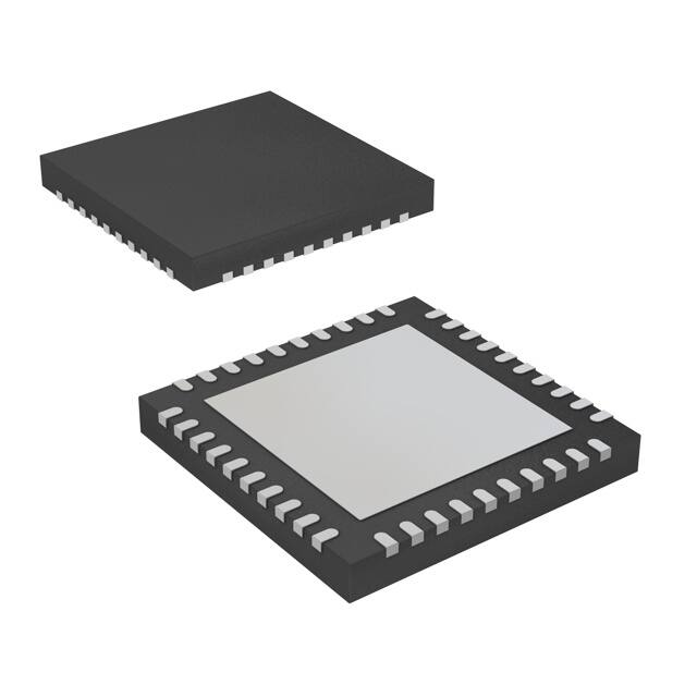
• 40 接线超薄型四方扁平无引线 (WQFN) 封装 (6mm
x 6mm)
LMK00338 器件是一款 8 路输出 PCIe 第 1 代/第 2 代/
第 3 代/第 4 代/第 5 代扇出缓冲器,旨在用于高频、低
抖动时钟、数据分配和电平转换。可从两个通用输入或
一个晶振输入中选择输入时钟。所选择的输入时钟被分
配到两组 HCSL 输出(每组 4 个)和 1 个 LVCMOS
输出。LVCMOS 输出具有同步使能输入,在使能或禁
用后可实现无短脉冲运行。LMK00338 由一个 3.3V 内
核电源和三个独立的 3.3V 或 2.5V 输出电源供电运
行。
2 应用
LMK00338 具有高性能、多用途和电源效率特性,这
使得它成为替代固定输出缓冲器器件的理想选择,同时
还能够增加系统中的时序余裕。
器件信息(1)
器件型号
LMK00338
(1)
封装
WQFN (40)
封装尺寸(标称值)
6.00mm × 6.00mm
如需了解所有可用封装,请参阅数据表末尾的可订购产品附
录。
CLKoutA_EN
• 面向 ADC、DAC、多千兆以太网、XAUI、光纤通
道、SATA/SAS、SONET/SDH、CPRI 和高频背板
的时钟分配和电平转换
• 交换机、路由器、线路接口卡、定时卡
• 服务器、计算、PCI Express(PCIe 3.0、4.0、
5.0)
• 远程无线电单元和基带单元
CLKoutB_EN
Copyright © 2017, Texas Instruments Incorporated
LMK00338 功能方框图
本文档旨在为方便起见,提供有关 TI 产品中文版本的信息,以确认产品的概要。有关适用的官方英文版本的最新信息,请访问
www.ti.com,其内容始终优先。TI 不保证翻译的准确性和有效性。在实际设计之前,请务必参考最新版本的英文版本。
English Data Sheet: SNAS636
�LMK00338
www.ti.com.cn
ZHCSCZ6C – DECEMBER 2013 – REVISED JULY 2021
Table of Contents
1 特性................................................................................... 1
2 应用................................................................................... 1
3 说明................................................................................... 1
4 Revision History.............................................................. 2
5 Pin Configuration and Functions...................................3
6 Specifications.................................................................. 5
6.1 Absolute Maximum Ratings........................................ 5
6.2 ESD Ratings............................................................... 5
6.3 Recommended Operating Conditions.........................5
6.4 Thermal Information....................................................5
6.5 Electrical Characteristics.............................................6
6.6 Typical Characteristics.............................................. 11
7 Parameter Measurement Information.......................... 13
7.1 Differential Voltage Measurement Terminology........ 13
8 Detailed Description......................................................14
8.1 Overview................................................................... 14
8.2 Functional Block Diagram......................................... 14
8.3 Feature Description...................................................14
8.4 Device Functional Modes..........................................16
9 Power Supply Recommendations................................22
9.1 Current Consumption and Power Dissipation
Calculations.................................................................22
9.2 Power Supply Bypassing.......................................... 23
10 Layout...........................................................................25
10.1 Layout Guidelines................................................... 25
10.2 Layout Example...................................................... 25
10.3 Thermal Management.............................................26
11 Device and Documentation Support..........................27
11.1 Documentation Support.......................................... 27
11.2 接收文档更新通知................................................... 27
11.3 支持资源..................................................................27
11.4 Trademarks............................................................. 27
11.5 静电放电警告...........................................................27
11.6 术语表..................................................................... 27
4 Revision History
注:以前版本的页码可能与当前版本的页码不同
Changes from Revision B (June 2017) to Revision C (July 2021)
Page
• 将数据表标题从 LMK00338 8 路输出差动时钟缓冲器和电平转换器 更改为:LMK00338 8 路输出 PCIe 第 1
代/第 2 代/第 3 代/第 4 代/第 5 代时钟缓冲器和电平转换器 ...............................................................................1
• 更改了目标应用,方法为将附加应用添加到第二个和第三个要点,并且从第一个要点中删除高速和串行接口。
............................................................................................................................................................................1
• 在数据表中添加了 PCIe 第 5 代..........................................................................................................................1
• Added PCIe 4.0 compliance data....................................................................................................................... 6
• Added additive RMS phase jitter for PCIe 4.0 and PCIe 5.0 to the Electrical Characteristics table................... 6
• Removed the LVPECL Phase Noise at 100 MHz graph .................................................................................. 11
• Changed the third paragraph in Driving the Clock Inputs section to include CLKin* and LVCMOS text.
Revised to better correspond with information in the Electrical Characteristics table...................................... 17
• Changed the bypass cap text to signal attenuation text of the fourth paragraph in Driving the Clock Inputs
section.............................................................................................................................................................. 17
• Changed the Single-Ended LVCMOS Input, DC Coupling with Common Mode Biasing image with revised
graphic.............................................................................................................................................................. 17
Changes from Revision A (October 2014) to Revision B (June 2017)
Page
• 已将整个数据表中的 CLKoutA_EN 和 CLKoutB_EN 引脚更改为 CLKoutA_EN 和 CLKoutB_EN .....................1
Changes from Revision * (December 2013) to Revision A (October 2014)
Page
• 添加、更新或重命名了以下各个部分:器件信息表、应用和实施;电源建议;布局;器件和文档支持;机械、
封装和可订购信息 .............................................................................................................................................. 1
• Added PCIE Gen4 additive jitter to the Electrical Characteristics table .............................................................6
• Changed 1 MHz to 12 kHz .................................................................................................................................6
• Added 图 10-1 ..................................................................................................................................................25
2
Submit Document Feedback
Copyright © 2022 Texas Instruments Incorporated
Product Folder Links: LMK00338
�LMK00338
www.ti.com.cn
ZHCSCZ6C – DECEMBER 2013 – REVISED JULY 2021
REFout
VCC
CLKin1
CLKin1*
VCC
GND
39
REFout_EN
VCC
40
VCCOC
GND
5 Pin Configuration and Functions
38
37
36
35
34
33
32
31
CLKoutA0
1
30
CLKoutB0
CLKoutA0*
2
29
CLKoutB0*
VCCOA
3
28
VCCOB
CLKoutA1
4
27
CLKoutB1
CLKoutA1*
5
26
CLKoutB1*
VCCOA
6
25
VCCOB
CLKoutA2
7
24
CLKoutB2
CLKoutA2*
8
23
CLKoutB2*
22
CLKoutB3
21
CLKoutB3*
Top Down View
13
14
15
16
17
18
19
CLKin0*
CLKin_SEL1
CLKoutB_EN
20
GND
12
CLKin0
CLKoutA_EN
11
CLKin_SEL0
10
OSCout
CLKoutA3*
VCC
9
OSCin
CLKoutA3
DAP
图 5-1. RTA Package 40-Pin WQFN Top View
表 5-1. Pin Functions(3)
PIN
NAME
DAP
NO.
TYPE
DESCRIPTION
DAP
GND
Die Attach Pad. Connect to the PCB ground plane for heat dissipation.
CLKin0
16
I
Universal clock input 0 (differential/single-ended)
CLKin0*
17
I
Universal clock input 0 (differential/single-ended)
CLKin1
34
I
Universal clock input 1 (differential/single-ended)
CLKin1*
33
I
Universal clock input 1 (differential/single-ended)
CLKoutA_EN
11
I
Bank A low active output buffer enable(2)
CLKoutA0
1
O
Differential clock output A0.
CLKoutA0*
2
O
Differential clock output A0.
CLKoutA1
4
O
Differential clock output A1.
CLKoutA1*
5
O
Differential clock output A1.
CLKoutA2
7
O
Differential clock output A2.
CLKoutA2*
8
O
Differential clock output A2.
CLKoutA3
9
O
Differential clock output A3.
CLKoutA3*
10
O
Differential clock output A3.
CLKoutB_EN
19
I
Bank B low active output buffer enable(2)
CLKoutB1
27
O
Differential clock output B1.
CLKoutB1*
26
O
Differential clock output B1.
CLKoutB0
30
O
Differential clock output B0.
CLKoutB0*
29
O
Differential clock output B0.
CLKoutB2
24
O
Differential clock output B2.
CLKoutB2*
23
O
Differential clock output B2.
CLKoutB3
22
O
Differential clock output B3.
Submit Document Feedback
Copyright © 2022 Texas Instruments Incorporated
Product Folder Links: LMK00338
3
�LMK00338
www.ti.com.cn
ZHCSCZ6C – DECEMBER 2013 – REVISED JULY 2021
表 5-1. Pin Functions(3) (continued)
PIN
NAME
TYPE
DESCRIPTION
CLKoutB3*
21
O
Differential clock output B3.
CLKin_SEL0
15
I
Clock input selection pins (2)
CLKin_SEL1
18
I
Clock input selection pins (2)
20, 31, 40
GND
GND
Ground
OSCin
13
I
Input for crystal. Can also be driven by a XO, TCXO, or other external single-ended clock.
OSCout
14
O
Output for crystal. Leave OSCout floating if OSCin is driven by a single-ended clock.
REFout
36
O
LVCMOS reference output. Enable output by pulling REFout_EN pin high.
REFout_EN
38
I
REFout enable input. Enable signal is internally synchronized to selected clock input.(2)
12, 32,
35, 39
PWR
Power supply for Core and Input buffer blocks. The VCC supply operates from 3.3 V.
Bypass with a 0.1-µF low-ESR capacitor placed very close to each VCC pin.
VCCOA
3, 6
PWR
Power supply for Bank A Output buffers. VCCOA can operate from 3.3 V or 2.5 V. The
VCCOA pins are internally tied together. Bypass with a 0.1-µF low-ESR capacitor placed
very close to each VCCO pin. (1)
VCCOB
25, 28
PWR
Power supply for Bank B Output buffers. VCCOB can operate from 3.3 V or 2.5 V. The
VCCOB pins are internally tied together. Bypass with a 0.1-µF low-ESR capacitor placed
very close to each VCCO pin. (1)
VCCOC
37
PWR
Power supply for REFout Output buffer. VCCOC can operate from 3.3 V or 2.5 V. Bypass
with a 0.1-µF low-ESR capacitor placed very close to each VCCO pin.(1)
VCC
(1)
(2)
(3)
4
NO.
The output supply voltages/pins (VCCOA, VCCOB, and VCCOC) is referred to generally as VCCO when no distinction is needed, or when
the output supply can be inferred by the output bank/type.
CMOS control input with internal pull-down resistor.
Any unused output pins should be left floating with minimum copper length (see note in Clock Outputs), or properly terminated if
connected to a transmission line, or disabled/Hi-Z if possible. See Clock Outputs for output configuration or Termination and Use of
Clock Drivers output interface and termination techniques.
Submit Document Feedback
Copyright © 2022 Texas Instruments Incorporated
Product Folder Links: LMK00338
�LMK00338
www.ti.com.cn
ZHCSCZ6C – DECEMBER 2013 – REVISED JULY 2021
6 Specifications
6.1 Absolute Maximum Ratings
over operating free-air temperature range (unless otherwise noted) (1) (2)
MIN
MAX
UNIT
Supply voltages
–0.3
3.6
V
VIN
Input voltage
–0.3
(VCC + 0.3)
V
TL
Lead temperature (solder 4 s)
260
°C
TJ
Junction temperature
150
°C
Tstg
Storage temperature
150
°C
VCC,
VCCO
(1)
(2)
–65
Stresses beyond those listed under Absolute Maximum Ratings may cause permanent damage to the device. These are stress ratings
only, which do not imply functional operation of the device at these or any other conditions beyond those indicated under
Recommended Operating Conditions. Exposure to absolute-maximum-rated conditions for extended periods may affect device
reliability.
If Military/Aerospace specified devices are required, please contact the Texas Instruments Sales Office/Distributors for availability and
specifications.
6.2 ESD Ratings
VALUE
Human-body model (HBM), per ANSI/ESDA/JEDEC
Electrostatic
discharge
V(ESD)
(1)
(2)
JS-001(1)
UNIT
±2000
Charged-device model (CDM), per JEDEC specification JESD22-C101(2)
±750
Machine model (MM)
±150
V
JEDEC document JEP155 states that 500-V HBM allows safe manufacturing with a standard ESD control process.
JEDEC document JEP157 states that 250-V CDM allows safe manufacturing with a standard ESD control process.
6.3 Recommended Operating Conditions
TA
Ambient temperature
TJ
Junction temperature
VCC
Core supply voltage
VCCO
Output supply voltage(1) (2)
(1)
(2)
3.3-V range
2.5-V range
MIN
TYP
MAX
–40
25
85
UNIT
°C
125
°C
3.15
3.3
3.45
V
3.3 – 5%
3.3
3.3 + 5%
2.5 – 5%
2.5
2.5 + 5%
V
The output supply voltages/pins (VCCOA, VCCOB, and VCCOC) will be referred to generally as VCCO when no distinction is needed, or
when the output supply can be inferred by the output bank/type.
VCCO should be less than or equal to VCC (VCCO ≤ VCC).
6.4 Thermal Information
LMK00338
THERMAL METRIC(1)
RTA (WQFN)
40
RθJA
Junction-to-ambient thermal resistance
RθJC(top)
Junction-to-case (top) thermal resistance
(1)
(2)
UNIT
PINS(2)
31.4
°C/W
7.2 (DAP)
°C/W
For more information about traditional and new thermal metrics, see the IC Package Thermal Metrics application report.
Specification assumes 9 thermal vias connect the die attach pad (DAP) to the embedded copper plane on the 4-layer JEDEC board.
These vias play a key role in improving the thermal performance of the package. TI recommends using the maximum number of vias in
the board layout.
Submit Document Feedback
Copyright © 2022 Texas Instruments Incorporated
Product Folder Links: LMK00338
5
�LMK00338
www.ti.com.cn
ZHCSCZ6C – DECEMBER 2013 – REVISED JULY 2021
6.5 Electrical Characteristics
Unless otherwise specified: VCC = 3.3 V ± 5%, VCCO = 3.3 V ± 5%, 2.5 V ± 5%, –40°C ≤ TA ≤ 85°C, CLKin driven
differentially, input slew rate ≥ 3 V/ns. Typical values represent most likely parametric norms at VCC = 3.3 V, VCCO = 3.3 V,
TA = 25°C, and at the Recommended Operating Conditions at the time of product characterization and are not ensured.(1) (2)
PARAMETER
TEST CONDITIONS
MIN
TYP
MAX
UNIT
CLKinX selected
8.5
10.5
mA
OSCin selected
10
13.5
mA
ICC_HCSL
31
38.5
mA
ICC_CMOS
3.5
5.5
mA
68
84
mA
VCCO = 3.3 V ±5%
9
10
mA
VCCO = 2.5V ± 5%
7
8
mA
CURRENT CONSUMPTION (3)
ICC_CORE
Core supply current, all outputs
disabled
ICCO_HCSL
Includes Output Bank Bias and Load Currents
Additive output supply current, HCSL
for both banks, RT = 50 Ω on all outputs in
banks enabled
bank
ICCO_CMOS
Additive output supply current,
LVCMOS output enabled
200 MHz,
CL = 5 pF
POWER SUPPLY RIPPLE REJECTION (PSRR)
PSRRHCSL
Ripple-induced phase spur level(4)
Differential HCSL output
156.25 MHz
–72
312.5 MHz
–63
dBc
CMOS CONTROL INPUTS (CLKin_SELn, CLKout_TYPEn, REFout_EN)
VIH
High-level input voltage
1.6
Vcc
V
VIL
Low-level input voltage
GND
0.4
V
IIH
High-level input current
VIH = VCC, internal pulldown resistor
50
μA
IIL
Low-level input current
VIL = 0 V, internal pulldown resistor
–5
Functional up to 400 MHz
Output frequency range and timing specified
per output type (refer to HCSL, LVCMOS
output specifications)
DC
0.1
μA
CLOCK INPUTS (CLKin0/CLKin0*, CLKin1/CLKin1*)
fCLKin
Input frequency
VIHD
Differential input high voltage
VILD
Differential input low voltage
VID
Differential input voltage swing(5)
VCMD
6
range(10)
Differential input CMD commonmode voltage
VIH
Single-ended input IH high voltage
VIL
Single-ended input IL low voltage
swing(14)
VI_SE
Single-ended input voltage
VCM
Single-ended input CM commonmode voltage
CLKin driven differentially
400
MHz
VCC
V
GND
V
0.15
1.3
VID = 150 mV
0.25
VCC –
1.2
VID = 350 mV
0.25
VCC –
1.1
VID = 800 mV
0.25
VCC –
0.9
CLKinX driven single-ended (AC- or DCcoupled), CLKinX* AC-coupled to GND or
externally biased within VCM range
GND
VCC
Submit Document Feedback
V
V
V
V
0.3
2
0.25
VCC –
1.2
Vpp
V
Copyright © 2022 Texas Instruments Incorporated
Product Folder Links: LMK00338
�LMK00338
www.ti.com.cn
ZHCSCZ6C – DECEMBER 2013 – REVISED JULY 2021
Unless otherwise specified: VCC = 3.3 V ± 5%, VCCO = 3.3 V ± 5%, 2.5 V ± 5%, –40°C ≤ TA ≤ 85°C, CLKin driven
differentially, input slew rate ≥ 3 V/ns. Typical values represent most likely parametric norms at VCC = 3.3 V, VCCO = 3.3 V,
TA = 25°C, and at the Recommended Operating Conditions at the time of product characterization and are not ensured.(1) (2)
PARAMETER
ISOMUX
Mux isolation, CLKin0 to CLKin1
TEST CONDITIONS
fOFFSET > 50 kHz,
PCLKinX = 0 dBm
fCLKin0 = 100 MHz
MIN
TYP
–84
MAX
UNIT
dBc
Submit Document Feedback
Copyright © 2022 Texas Instruments Incorporated
Product Folder Links: LMK00338
7
�LMK00338
www.ti.com.cn
ZHCSCZ6C – DECEMBER 2013 – REVISED JULY 2021
Unless otherwise specified: VCC = 3.3 V ± 5%, VCCO = 3.3 V ± 5%, 2.5 V ± 5%, –40°C ≤ TA ≤ 85°C, CLKin driven
differentially, input slew rate ≥ 3 V/ns. Typical values represent most likely parametric norms at VCC = 3.3 V, VCCO = 3.3 V,
TA = 25°C, and at the Recommended Operating Conditions at the time of product characterization and are not ensured.(1) (2)
PARAMETER
TEST CONDITIONS
MIN
TYP
fCLKin0 = 200 MHz
–82
fCLKin0 = 500 MHz
–71
fCLKin0 = 1000 MHz
–65
MAX
UNIT
250
MHz
40
MHz
CRYSTAL INTERFACE (OSCin, OSCout)
FCLK
External clock frequency range(10)
OSCin driven single-ended, OSCout floating
FXTAL
Crystal frequency range
Fundamental mode crystal ESR ≤ 200 Ω (10
to 30 MHz) ESR ≤ 125 Ω (30 to 40 MHz)(6)
CIN
OSCin input capacitance
10
1
pF
HCSL OUTPUTS (CLKoutAn/CLKoutAn*, CLKoutBn/CLKoutBn*)
fCLKout
Output frequency range(10)
RL = 50 Ω to GND, CL ≤ 5 pF
JitterADD_PCle
Additive RMS phase jitter for PCIe
5.0(10)
PCIe Gen 5 filter
CLKin: 100 MHz,
Slew rate ≥ 0.5 V/ns
JitterADD_PCle
Additive RMS phase jitter for PCIe
4.0(10)
PCIe Gen 4,
PLL BW = 2–5 MHz,
CDR = 10 MHz
JitterADD_PCle
Additive RMS phase jitter for PCIe
3.0(10)
PCIe Gen 3,
PLL BW = 2–5 MHz,
CDR = 10 MHz
JitterADD
Additive RMS jitter integration
bandwidth to 20 MHz(8) (9)
VCCO = 3.3 V,
RT = 50 Ω to GND
Noise Floor
8
Noise floor fOFFSET ≥ 10
MHz(8) (9)
VCCO = 3.3 V,
RT = 50 Ω to GND
400
MHz
0.015
0.03
ps
CLKin: 100 MHz,
Slew rate ≥ 1.8 V/ns
0.03
0.05
ps
CLKin: 100 MHz,
Slew rate ≥ 0.6 V/ns
0.03
0.15
ps
CLKin: 100 MHz,
Slew rate ≥ 3 V/ns
77
CLKin: 156.25 MHz,
Slew rate ≥ 2.7 V/ns
86
–161.3
CLKin: 156.25 MHz,
Slew rate ≥ 2.7 V/ns
–156.3
Duty cycle(10)
50% input clock duty cycle
VOH
Output high voltage
VOL
Output low voltage
TA = 25°C, DC measurement,
RT = 50 Ω to GND
VCROSS
Absolute crossing
ΔVCROSS
Total variation of VCROSS
tR
Output rise time 20% to 80%(11) (14)
tF
Output fall time 80% to 20%(11) (14)
fs
CLKin: 100 MHz,
Slew rate ≥ 3 V/ns
DUTY
voltage(10) (11)
DC
45%
RL = 50 Ω to GND,
CL ≤ 5 pF
250 MHz, uniform transmission line up to 10 in.
with 50-Ω characteristic impedance,
RL = 50 Ω to GND, CL ≤ 5 pF
Submit Document Feedback
dBc/Hz
55%
520
810
920
mV
–150
0.5
150
mV
160
350
460
mV
140
mV
300
500
ps
300
500
ps
Copyright © 2022 Texas Instruments Incorporated
Product Folder Links: LMK00338
�LMK00338
www.ti.com.cn
ZHCSCZ6C – DECEMBER 2013 – REVISED JULY 2021
Unless otherwise specified: VCC = 3.3 V ± 5%, VCCO = 3.3 V ± 5%, 2.5 V ± 5%, –40°C ≤ TA ≤ 85°C, CLKin driven
differentially, input slew rate ≥ 3 V/ns. Typical values represent most likely parametric norms at VCC = 3.3 V, VCCO = 3.3 V,
TA = 25°C, and at the Recommended Operating Conditions at the time of product characterization and are not ensured.(1) (2)
PARAMETER
TEST CONDITIONS
MIN
TYP
MAX
UNIT
250
MHz
LVCMOS OUTPUT (REFout)
fCLKout
Output frequency range(10)
CL ≤ 5 pF
JitterADD
Additive RMS jitter integration
bandwidth 1 MHz to 20 MHz(7)
VCCO = 3.3 V,
CL ≤ 5 pF
100 MHz,
Input slew rate ≥ 3
V/ns
95
Noise Floor
Noise floor fOFFSET ≥ 10 MHz(8) (9)
VCCO = 3.3 V,
CL ≤ 5 pF
100 MHz,
Input slew rate ≥ 3
V/ns
–159.3
DUTY
Duty cycle(10)
50% input clock duty cycle
VOH
Output high voltage
VOL
Output low voltage
IOH
Output high current (source)
IOL
Output low current (sink)
tR
Output rise time 20% to 80%(11) (14)
tF
Output fall time 80% to 20%(11) (14)
tEN
Output enable time(12)
tDIS
Output disable time(12)
DC
45%
fs
dBc/Hz
55%
VCCO
– 0.1
1-mA load
V
0.1
VO = VCCO / 2
VCCO = 3.3 V
28
VCCO = 2.5 V
20
VCCO = 3.3 V
28
VCCO = 2.5 V
20
250 MHz, uniform transmission line up to 10 in.
with 50-Ω characteristic impedance, RL = 50
Ω to GND, CL ≤ 5 pF
V
mA
mA
225
400
ps
225
400
ps
CL ≤ 5 pF
3
cycles
3
cycles
PROPAGATION DELAY and OUTPUT SKEW
tPD_HCSL
Propagation delay CLKin-to-HCSL(11) RT = 50 Ω to GND,
(14)
CL ≤ 5 pF
tPD_CMOS
Propagation delay CLKin-toLVCMOS(11) (14)
tSK(O)
Output skew(10) (11) (13)
tSK(PP)
Part-to-part output skew
HCSL(11) (14) (13)
(1)
(2)
(3)
(4)
(5)
(6)
(7)
(8)
CL ≤ 5 pF
295
590
885
VCCO = 3.3 V
900
1475
2300
VCCO = 2.5 V
1000
1550
2700
30
50
ps
80
120
ps
Skew specified between any two CLKouts.
Load conditions are the same as propagation
delay specifications.
ps
ps
The output supply voltages/pins (VCCOA, VCCOB, and VCCOC) will be referred to generally as VCCO when no distinction is needed, or
when the output supply can be inferred by the output bank/type.
The Electrical Characteristics tables list ensured specifications under the listed Recommended Operating Conditions except as
otherwise modified or specified by the Electrical Characteristics conditions and notes. Typical specifications are estimations only and
are not ensured.
See Power Supply Recommendations for more information on current consumption and power dissipation calculations.
Power supply ripple rejection, or PSRR, is defined as the single-sideband phase spur level (in dBc) modulated onto the clock output
when a single-tone sinusoidal signal (ripple) is injected onto the VCCO supply. Assuming no amplitude modulation effects and small
index modulation, the peak-to-peak deterministic jitter (DJ) can be calculated using the measured single-sideband phase spur level
(PSRR) as follows: DJ (ps pk-pk) = [ (2 × 10(PSRR / 20)) / (π × fCLK) ] × 1E12
See Differential Voltage Measurement Terminology for definition of VID and VOD voltages.
The ESR requirements stated must be met to ensure that the oscillator circuitry has no start-up issues. However, lower ESR values for
the crystal may be necessary to stay below the maximum power dissipation (drive level) specification of the crystal. Refer to Crystal
Interface for crystal drive level considerations.
For the 100-MHz and 156.25-MHz clock input conditions, Additive RMS Jitter (JADD) is calculated using Method #1: JADD = SQRT(JOUT
2–J
2
SOURCE ), where JOUT is the total RMS jitter measured at the output driver and JSOURCE is the RMS jitter of the clock source
applied to CLKin. For the 625-MHz clock input condition, additive RMS jitter is approximated using Method #2: JADD = SQRT(2 ×
10dBc/10) / (2 × π × fCLK), where dBc is the phase noise power of the output noise floor integrated from 1-MHz to 20-MHz bandwidth.
The phase noise power can be calculated as: dBc = Noise Floor + 10 × log10(20 MHz – 1 MHz). The additive RMS jitter was
approximated for 625 MHz using Method #2 because the RMS jitter of the clock source was not sufficiently low enough to allow
practical use of Method #1. Refer to the Noise Floor vs. CLKin Slew Rate and RMS Jitter vs. CLKin Slew Rate plots in Typical
Characteristics.
The noise floor of the output buffer is measured as the far-out phase noise of the buffer. Typically this offset is ≥ 10 MHz, but for lower
frequencies this measurement offset can be as low as 5 MHz due to measurement equipment limitations.
Submit Document Feedback
Copyright © 2022 Texas Instruments Incorporated
Product Folder Links: LMK00338
9
�LMK00338
www.ti.com.cn
ZHCSCZ6C – DECEMBER 2013 – REVISED JULY 2021
(9)
(10)
(11)
(12)
(13)
(14)
10
Phase noise floor will degrade as the clock input slew rate is reduced. Compared to a single-ended clock, a differential clock input
(LVPECL, LVDS) is less susceptible to degradation in noise floor at lower slew rates due to its common-mode noise rejection.
However, TI recommends using the highest possible input slew rate for differential clocks to achieve optimal noise floor performance at
the device outputs.
Specification is ensured by characterization and is not tested in production.
AC timing parameters for HCSL or CMOS are dependent on output capacitive loading.
Output enable time is the number of input clock cycles it takes for the output to be enabled after REFout_EN is pulled high. Similarly,
output disable time is the number of input clock cycles it takes for the output to be disabled after REFout_EN is pulled low. The
REFout_EN signal should have an edge transition much faster than that of the input clock period for accurate measurement.
Output skew is the propagation delay difference between any two outputs with identical output buffer type and equal loading while
operating at the same supply voltage and temperature conditions.
Parameter is specified by design, not tested in production.
Submit Document Feedback
Copyright © 2022 Texas Instruments Incorporated
Product Folder Links: LMK00338
�LMK00338
www.ti.com.cn
ZHCSCZ6C – DECEMBER 2013 – REVISED JULY 2021
6.6 Typical Characteristics
Unless otherwise specified: VCC = 3.3 V, VCCO = 3.3 V, TA = 25°C, CLKin driven differentially, input slew rate ≥ 3
V/ns.
1.0
1.00
Output Swing (V)
0.8
Output Swing (V)
Vcco=3.3 V, AC coupled, 50
Vcco=2.5 V, AC coupled, 50
0.75
0.6
0.4
0.2
load
load
0.50
0.25
0.00
-0.25
-0.50
0.0
-0.75
-0.2
-1.00
0
1
2
3
Time (ns)
4
5
图 6-1. HCSL Output Swing at 250 MHz
Noise Floor (dBc/Hz)
-145
-135
HCSL
LVCMOS
CLKin Source
-155
-160
-165
6
HCSL
CLKin Source
-150
-155
-165
Foffset = 20 MHz
0.5
1.0
1.5
2.0
2.5
3.0
3.5
Differential Input Slew Rate (V/ns)
Fclk = 156.25 MHz
图 6-3. Noise Floor vs CLKin Slew Rate at 100 MHz
Foffset = 20 MHz
图 6-4. Noise Floor vs CLKin Slew Rate at 156.25
MHz
500
HCSL
LVCMOS
CLKin Source
450
HCSL
CLKin Source
400
RMS Jitter (fs)
300
RMS Jitter (fs)
5
-145
1.0
1.5
2.0
2.5
3.0
3.5
Differential Input Slew Rate (V/ns)
Fclk = 100 MHz
350
3
4
Time (ns)
-160
-170
400
2
-140
-150
0.5
1
图 6-2. LVCMOS Output Swing at 250 MHz
Noise Floor (dBc/Hz)
-140
0
250
200
150
100
350
300
250
200
150
100
50
50
0
0
0.5
1.0
1.5
2.0
2.5
3.0
3.5
Differential Input Slew Rate (V/ns)
Fclk = 100 MHz
Int. BW = 1 to 20 MHz
图 6-5. RMS Jitter vs CLKin Slew Rate at 100 MHz
0.5
1.0
1.5
2.0
2.5
3.0
3.5
Differential Input Slew Rate (V/ns)
Fclk = 156.25 MHz
Int. BW = 1 to 20 MHz
图 6-6. RMS Jitter vs CLKin Slew Rate at 156.25
MHz
Submit Document Feedback
Copyright © 2022 Texas Instruments Incorporated
Product Folder Links: LMK00338
11
�LMK00338
www.ti.com.cn
ZHCSCZ6C – DECEMBER 2013 – REVISED JULY 2021
-50
HCSL
Ripple Induced Spur Level (dBc)
Ripple Induced Spur Level (dBc)
-50
-55
-60
-65
-70
-75
-80
-85
-90
-60
-65
-70
-75
-80
-85
-90
1
Ripple Frequency (MHz)
Fclk = 156.25 MHz
10
VCCO Ripple = 100
图 6-7. PSRR vs Ripple Frequency at 156.25 MHz
1950
HCSL (0.35 ps/°C)
LVCMOS (2.2 ps/°C)
750
650
1850
Right Y-axis plot
1750
550
1650
450
1550
350
1450
250
1350
-50
-25
0
25
50
75
Temperature (°C)
REFout Propagation Delay (ps)
850
.1
10
VCCO Ripple = 100 mVpp
图 6-8. PSRR vs Ripple Frequency at 312.5 MHz
200
20 MHz Crystal
40 MHz Crystal
175
150
125
100
75
50
25
0
0
100
图 6-9. Propagation Delay vs Temperature
1
Ripple Frequency (MHz)
Fclk = 312.5 MHz
CRYSTAL POWER DISSIPATION ( W)
.1
CLKout Propagation Delay (ps)
HCSL
-55
500 1k 1.5k 2k 2.5k 3k 3.5k 4k
RLIM( )
图 6-10. Crystal Power Dissipation vs RLIM
图 6-11. HCSL Phase Noise at 100 MHz
12
Submit Document Feedback
Copyright © 2022 Texas Instruments Incorporated
Product Folder Links: LMK00338
�LMK00338
www.ti.com.cn
ZHCSCZ6C – DECEMBER 2013 – REVISED JULY 2021
7 Parameter Measurement Information
7.1 Differential Voltage Measurement Terminology
The differential voltage of a differential signal can be described by two different definitions causing confusion
when reading data sheets or communicating with other engineers. This section will address the measurement
and description of a differential signal so that the reader will be able to understand and discern between the two
different definitions when used.
The first definition used to describe a differential signal is the absolute value of the voltage potential between the
inverting and noninverting signal. The symbol for this first measurement is typically VID or VOD depending on if
an input or output voltage is being described.
The second definition used to describe a differential signal is to measure the potential of the noninverting signal
with respect to the inverting signal. The symbol for this second measurement is VSS and is a calculated
parameter. Nowhere in the IC does this signal exist with respect to ground; it only exists in reference to its
differential pair. VSS can be measured directly by oscilloscopes with floating references, otherwise this value can
be calculated as twice the value of VOD as described above.
图 7-1 illustrates the two different definitions side-by-side for inputs and 图 7-2 illustrates the two different
definitions side-by-side for outputs. The VID (or VOD) definition show the DC levels, VIH and VOL (or VOH and
VOL), that the noninverting and inverting signals toggle between with respect to ground. VSS input and output
definitions show that if the inverting signal is considered the voltage potential reference, the noninverting signal
voltage potential is now increasing and decreasing above and below the noninverting reference. Thus the peakto-peak voltage of the differential signal can be measured.
VID and VOD are often defined as volts (V) and VSS is often defined as volts peak-to-peak (VPP).
VID Definition
VSS Definition for Input
Noninverting Clock
VIH
VCM
VSS
VID
VIL
Inverting Clock
VID = | VIH ± VIL |
VSS = 2 × VID
GND
图 7-1. Two Different Definitions for Differential Input Signals
VOD Definition
VSS Definition for Output
Noninverting Clock
VOH
VOS
VSS
VOD
VOL
Inverting Clock
VOD = | VOH s VOL |
VSS = 2 × VOD
GND
图 7-2. Two Different Definitions for Differential Output Signals
Refer to AN-912 Common Data Transmission Parameters and their Definitions (SNLA036) for more information.
Submit Document Feedback
Copyright © 2022 Texas Instruments Incorporated
Product Folder Links: LMK00338
13
�LMK00338
www.ti.com.cn
ZHCSCZ6C – DECEMBER 2013 – REVISED JULY 2021
8 Detailed Description
8.1 Overview
The LMK00338 is an 8-output PCIe Gen1/Gen2/Gen3/Gen4/Gen5 clock fanout buffer with low additive jitter that
can operate up to 400 MHz. It features a 3:1 input multiplexer with an optional crystal oscillator input, two banks
of 4 HCSL outputs, one LVCMOS output, and 3 independent output buffer supplies. The input selection and
output buffer modes are controlled through pin strapping. The device is offered in a 40-pin WQFN package and
leverages much of the high-speed, low-noise circuit design employed in the LMK04800 family of clock
conditioners.
8.2 Functional Block Diagram
CLKoutA_EN
CLKoutB_EN
Copyright © 2017, Texas Instruments Incorporated
8.3 Feature Description
8.3.1 Crystal Power Dissipation vs. RLIM
For 图 6-10, the following applies:
• The typical RMS jitter values in the plots show the total output RMS jitter (JOUT) for each output buffer type
and the source clock RMS jitter (JSOURCE). From these values, the Additive RMS Jitter can be calculated as:
JADD = SQRT(JOUT 2 – JSOURCE 2)
• 20-MHz crystal characteristics: Abracon ABL series, AT cut, CL = 18 pF , C0 = 4.4 pF measured (7 pF
maximum), ESR = 8.5 Ω measured (40 Ω maximum), and Drive Level = 1 mW maximum (100 µW typical).
40-MHz crystal characteristics: Abracon ABLS2 series, AT cut, CL = 18 pF , C0 = 5 pF measured (7 pF
maximum), ESR = 5 Ω measured (40 Ω maximum), and Drive Level = 1 mW maximum (100 µW typical).
14
Submit Document Feedback
Copyright © 2022 Texas Instruments Incorporated
Product Folder Links: LMK00338
�LMK00338
www.ti.com.cn
ZHCSCZ6C – DECEMBER 2013 – REVISED JULY 2021
8.3.2 Clock Inputs
The input clock can be selected from CLKin0/CLKin0*, CLKin1/CLKin1*, or OSCin. Clock input selection is
controlled using the CLKin_SEL[1:0] inputs as shown in 表 8-1. Refer to Driving the Clock Inputs for clock input
requirements. When CLKin0 or CLKin1 is selected, the crystal circuit is powered down. When OSCin is selected,
the crystal oscillator circuit will start up and its clock will be distributed to all outputs. Refer to Crystal Interface for
more information. Alternatively, OSCin may be driven by a single-ended clock (up to 250 MHz) instead of a
crystal.
表 8-1. Input Selection
CLKin_SEL1
CLKin_SEL0
SELECTED INPUT
0
0
CLKin0, CLKin0*
0
1
CLKin1, CLKin1*
1
X
OSCin
表 8-2 shows the output logic state vs input state when either CLKin0/CLKin0* or CLKin1/CLKin1* is selected.
When OSCin is selected, the output state becomes an inverted copy of the OSCin input state.
表 8-2. CLKin Input vs Output States
STATE of
SELECTED CLKin
STATE of
ENABLED OUTPUTS
CLKinX and CLKinX*
inputs floating
Logic low
CLKinX and CLKinX*
inputs shorted together
Logic low
CLKin logic low
Logic low
CLKin logic high
Logic high
8.3.3 Clock Outputs
The HCSL output buffer for Bank A and Bank B outputs can be separately disabled to Hi-Z using the
CLKoutA_EN and CLKoutB_EN inputs, respectively, as shown in 表 8-3. For applications where all differential
outputs are not needed, any unused output pin should be left floating with a minimum copper length (see note
below) to minimize capacitance and potential coupling and reduce power consumption. If an entire output bank
will not be used, TI recommends to disable and Hi-Z the bank to reduce power. Refer to Termination and Use of
Clock Drivers for more information on output interface and termination techniques.
Note
For best soldering practices, the minimum trace length for any unused output pin should extend to
include the pin solder mask. This way during reflow, the solder has the same copper area as
connected pins. This allows for good, uniform fillet solder joints helping to keep the IC level during
reflow.
表 8-3. Differential Output Buffer Type Selection
CLKoutX_EN
CLKoutX BUFFER TYPE
(BANK A or B)
0
HCSL
1
Disabled (Hi-Z)
Submit Document Feedback
Copyright © 2022 Texas Instruments Incorporated
Product Folder Links: LMK00338
15
�LMK00338
www.ti.com.cn
ZHCSCZ6C – DECEMBER 2013 – REVISED JULY 2021
8.3.3.1 Reference Output
The reference output (REFout) provides a LVCMOS copy of the selected input clock. The LVCMOS output high
level is referenced to the VCCO voltage. REFout can be enabled or disabled using the enable input pin,
REFout_EN, as shown in 表 8-4.
表 8-4. Reference Output Enable
REFout_EN
REFout STATE
0
Disabled (Hi-Z)
1
Enabled
The REFout_EN input is internally synchronized with the selected input clock by the SYNC block. This
synchronizing function prevents glitches and runt pulses from occurring on the REFout clock when enabled or
disabled. REFout is enabled within 3 cycles (tEN) of the input clock after REFout_EN is toggled high. REFout is
disabled within 3 cycles (tDIS) of the input clock after REFout_EN is toggled low.
When REFout is disabled, the use of a resistive loading can be used to set the output to a predetermined level.
For example, if REFout is configured with a 1-kΩ load to ground, then the output will be pulled to low when
disabled.
8.4 Device Functional Modes
8.4.1 VCC and VCCO Power Supplies
The LMK00338 has a 3.3-V core power supply (VCC) and 3 independent 3.3-V or 2.5-V output power supplies
(VCCOA, VCCOB, VCCOC). Output supply operation at 2.5 V enables lower power consumption and output-level
compatibility with 2.5-V receiver devices. The output levels for HCSL are relatively constant over the specified
VCCO range. Refer to Power Supply Recommendations for additional supply related considerations, such as
power dissipation, power supply bypassing, and power supply ripple rejection (PSRR).
Note
Take care to ensure the VCCO voltages do not exceed the VCC voltage to prevent turning-on the
internal ESD protection circuitry.
16
Submit Document Feedback
Copyright © 2022 Texas Instruments Incorporated
Product Folder Links: LMK00338
�LMK00338
www.ti.com.cn
ZHCSCZ6C – DECEMBER 2013 – REVISED JULY 2021
Application and Implementation
Note
以下应用部分的信息不属于 TI 组件规范,TI 不担保其准确性和完整性。客户应负责确定 TI 组件是否适
用于其应用。客户应验证并测试其设计,以确保系统功能。
9.1 Application Information
A common PCIe application, such as a server card, consists of several building blocks, which all need a
reference clock. In the mostly used Common RefClk architecture, the clock is distributed from a single source to
both RX and TX. This requires either a Clock generator with high output count or a buffer like the LMK00338.
The buffer simplifies the clocking tree and provides a cost and space optimized solution. While using a buffer to
distribute the clock, the additive jitter needs to be considered. The LMK00338 is an ultra-low additive jitter PCIe
clock buffer suitable for all current and future PCIe Generations.
9.2 Typical Application
Mainboard
MAC
100MHz
Reference
Oscillator
PCI Express®
PHY
E.g.: XIO1100
Fan Out Buffer
E.g.: LMK00338
PCI Express®
fan-out switch
E.g.: XIO3130
Connector
FPGA with
PCI Express®
Core
PCIExpress®
Express®
PCI
PCI
Express®
bridge
bridge
PCIE.g.:
Express®
bridge
XIO2000A
E.g.:
XIO2000A
device
E.g.: XIO2000A
Add-In Card
Add-In Card
Add-In Card
Add-In Card
Data
Clock
Copyright © 2017, Texas Instruments Incorporated
图 9-1. Example PCI Express Application Diagram
9.2.1 Design Requirements
9.2.1.1 Driving the Clock Inputs
The LMK00338 has two universal inputs (CLKin0/CLKin0* and CLKin1/CLKin1*) that can accept AC- or DCcoupled, 3.3-V and 2.5-V LVPECL, LVDS, CML, SSTL, and other differential and single-ended signals that meet
the input requirements specified in the Electrical Characteristics table. The device can accept a wide range of
signals due to its wide input common-mode voltage range (VCM ) and input voltage swing (VID) / dynamic range.
For 50% duty cycle and DC-balanced signals, AC coupling may also be employed to shift the input signal to
within the VCM range. Refer to Termination and Use of Clock Drivers for signal interfacing and termination
techniques.
Submit Document Feedback
Copyright © 2022 Texas Instruments Incorporated
Product Folder Links: LMK00338
17
�LMK00338
www.ti.com.cn
ZHCSCZ6C – DECEMBER 2013 – REVISED JULY 2021
To achieve the best possible phase noise and jitter performance, it is mandatory for the input to have high slew
rate of 3 V/ns (differential) or higher. Driving the input with a lower slew rate will degrade the noise floor and jitter.
For this reason, a differential signal input is recommended over single-ended because it typically provides higher
slew rate and common-mode rejection. Refer to the Noise Floor vs. CLKin Slew Rate and RMS Jitter vs. CLKin
Slew Rate plots in Typical Characteristics.
While TI recommends driving the CLKin/CLKin* pair with a differential signal input, it is possible to drive it with a
single-ended clock provided it conforms to the Single-Ended Input specifications for CLKin pins listed in the
Electrical Characteristics table. For large single-ended input signals, such as 3.3-V or 2.5-V LVCMOS, a 50-Ω
load resistor should be placed near the input for signal attenuation to prevent input overdrive as well as for line
termination to minimize reflections. Again, the single-ended input slew rate should be as high as possible to
minimize performance degradation. The CLKin input has an internal bias voltage of about 1.4 V, so the input can
be AC-coupled as shown in 图 9-2. The output impedance of the LVCMOS driver plus Rs should be close to 50
Ω to match the characteristic impedance of the transmission line and load termination.
RS 0.1 PF
0.1 PF
50: Trace
50:
CMOS
Driver
LMK
Input
0.1 PF
图 9-2. Single-Ended LVCMOS Input, AC Coupling
A single-ended clock may also be DC-coupled to CLKinX as shown in 图 9-3. A 50-Ω load resistor should be
placed near the CLKinX input for signal attenuation and line termination. Because half of the single-ended swing
of the driver (VO,PP / 2) drives CLKinX, CLKinX* should be externally biased to the midpoint voltage of the
attenuated input swing ((VO,PP / 2) × 0.5). The external bias voltage should be within the specified input common
voltage (VCM) range. This can be achieved using external biasing resistors in the kΩ range (RB1 and RB2) or
another low-noise voltage reference. This ensures the input swing crosses the threshold voltage at a point where
the input slew rate is the highest.
VO,PP
Rs
VO,PP/2
VCC
50: Trace
CMOS
Driver
50:
VBB ~ (VO,PP/2) x 0.5
LMK
Input
RB1
VCC
RB2
0.1 PF
图 9-3. Single-Ended LVCMOS Input, DC Coupling With Common-Mode Biasing
18
Submit Document Feedback
Copyright © 2022 Texas Instruments Incorporated
Product Folder Links: LMK00338
�LMK00338
www.ti.com.cn
ZHCSCZ6C – DECEMBER 2013 – REVISED JULY 2021
If the crystal oscillator circuit is not used, it is possible to drive the OSCin input with an single-ended external
clock as shown in 图 9-4. The input clock should be AC-coupled to the OSCin pin, which has an internallygenerated input bias voltage, and the OSCout pin should be left floating. While OSCin provides an alternative
input to multiplex an external clock, TI recommends using either differential input (CLKinX) because it offers
higher operating frequency, better common-mode and power supply noise rejection, and greater performance
over supply voltage and temperature variations.
0.1 PF
0.1 PF
50: Trace
50:
OSCin
OSCout
LMK00301
RS
CMOS
Driver
Copyright © 2017, Texas Instruments Incorporated
图 9-4. Driving OSCin With a Single-Ended Input
9.2.1.2 Crystal Interface
The LMK00338 has an integrated crystal oscillator circuit that supports a fundamental mode, AT-cut crystal. The
crystal interface is shown in 图 9-5.
C1
XTAL
RLIM
OSCout
LMK00301
OSCin
C2
Copyright © 2017, Texas Instruments Incorporated
图 9-5. Crystal Interface
The load capacitance (CL) is specific to the crystal, but usually on the order of 18 to 20 pF. While CL is specified
for the crystal, the OSCin input capacitance (CIN = 1 pF typical) of the device and PCB stray capacitance
(CSTRAY = 1 to approximately 3 pF) can affect the discrete load capacitor values, C1 and C2.
For the parallel resonant circuit, the discrete capacitor values can be calculated as follows:
CL = (C1 × C2) / (C1 + C2) + CIN + CSTRAY
(1)
Typically, C1 = C2 for optimum symmetry, so 方程式 1 can be rewritten in terms of C1 only:
CL = C1 2 / (2 × C1) + CIN + CSTRAY
(2)
Finally, solve for C1:
C1 = (CL – CIN – CSTRAY) × 2
(3)
Submit Document Feedback
Copyright © 2022 Texas Instruments Incorporated
Product Folder Links: LMK00338
19
�LMK00338
www.ti.com.cn
ZHCSCZ6C – DECEMBER 2013 – REVISED JULY 2021
The Electrical Characteristics table provides crystal interface specifications with conditions that ensure start-up
of the crystal, but it does not specify crystal power dissipation. The designer must ensure the crystal power
dissipation does not exceed the maximum drive level specified by the crystal manufacturer. Overdriving the
crystal can cause premature aging, frequency shift, and eventual failure. Drive level should be held at a sufficient
level necessary to start up and maintain steady-state operation.
The power dissipated in the crystal, PXTAL, can be computed by:
PXTAL = IRMS 2 × RESR × (1 + C0/CL)2
(4)
where
•
•
•
•
IRMS is the RMS current through the crystal.
RESR is the maximum equivalent series resistance specified for the crystal
CL is the load capacitance specified for the crystal
C0 is the minimum shunt capacitance specified for the crystal
IRMS can be measured using a current probe (for example, Tektronix CT-6 or equivalent) placed on the leg of the
crystal connected to OSCout with the oscillation circuit active.
As shown in 图 9-5, an external resistor, RLIM, can be used to limit the crystal drive level, if necessary. If the
power dissipated in the selected crystal is higher than the drive level specified for the crystal with RLIM shorted,
then a larger resistor value is mandatory to avoid overdriving the crystal. However, if the power dissipated in the
crystal is less than the drive level with RLIM shorted, then a zero value for RLIM can be used. As a starting point, a
suggested value for RLIM is 1.5 kΩ.
9.2.2 Detailed Design Procedure
9.2.2.1 Termination and Use of Clock Drivers
When terminating clock drivers keep in mind these guidelines for optimum phase noise and jitter performance:
• Transmission line theory should be followed for good impedance matching to prevent reflections.
• Clock drivers should be presented with the proper loads.
– HCSL drivers are switched current outputs and require a DC path to ground through 50-Ω termination.
• Receivers should be presented with a signal biased to their specified DC bias level (common-mode voltage)
for proper operation. Some receivers have self-biasing inputs that automatically bias to the proper voltage
level; in this case, the signal should normally be AC-coupled.
9.2.2.2 Termination for DC-Coupled Differential Operation
50:
For DC-coupled operation of an HCSL driver, terminate with 50 Ω to ground near the driver output as shown in
图 9-6. Series resistors, Rs, may be used to limit overshoot due to the fast transient current. Because HCSL
drivers require a DC path to ground, AC coupling is not allowed between the output drivers and the 50-Ω
termination resistors.
CLKoutX
HCSL
Driver
Rs
50: Traces
Rs
HCSL
Receiver
50:
CLKoutX*
图 9-6. HCSL Operation, DC Coupling
20
Submit Document Feedback
Copyright © 2022 Texas Instruments Incorporated
Product Folder Links: LMK00338
�LMK00338
www.ti.com.cn
ZHCSCZ6C – DECEMBER 2013 – REVISED JULY 2021
9.2.2.3 Termination for AC-Coupled Differential Operation
AC coupling allows for shifting the DC bias level (common-mode voltage) when driving different receiver
standards. Because AC coupling prevents the driver from providing a DC bias voltage at the receiver, it is
important to ensure the receiver is biased to its ideal DC level.
9.2.3 Application Curve
图 9-7. HCSL Phase Noise at 100 MHz
Submit Document Feedback
Copyright © 2022 Texas Instruments Incorporated
Product Folder Links: LMK00338
21
�LMK00338
www.ti.com.cn
ZHCSCZ6C – DECEMBER 2013 – REVISED JULY 2021
9 Power Supply Recommendations
9.1 Current Consumption and Power Dissipation Calculations
The current consumption values specified in the Electrical Characteristics table can be used to calculate the total
power dissipation and IC power dissipation for any device configuration. The total VCC core supply current
(ICC_TOTAL) can be calculated using 方程式 5:
ICC_TOTAL = ICC_CORE + ICC_BANK_A + ICC_BANK_B + ICC_CMOS
(5)
where
•
•
•
•
ICC_CORE is the current for core logic and input blocks and depends on selected input (CLKinX or OSCin).
ICC_BANK_A is the current for Bank A.
ICC_BANK_B is the current for Bank B.
ICC_CMOS is the current for the LVCMOS output (or 0 mA if REFout is disabled).
Because the output supplies (VCCOA, VCCOB, VCCOC) can be powered from 3 independent voltages, the
respective output supply currents (ICCO_BANK_A, ICCO_BANK_B, and ICCO_CMOS) should be calculated separately.
ICCO_BANK for either Bank A or B can be directly taken from the corresponding output supply current spec
(ICCO_HCSL) provided the output loading matches the specified conditions. Otherwise, ICCO_BANK should be
calculated as follows:
ICCO_BANK = IBANK_BIAS + (N × IOUT_LOAD)
(6)
where
• IBANK_BIAS is the output bank bias current (fixed value).
• IOUT_LOAD is the DC load current per loaded output pair.
• N is the number of loaded output pairs per bank (N = 0 to 4).
表 9-1 shows the typical IBANK_BIAS values and IOUT_LOAD expressions for HCSL.
表 9-1. Typical Output Bank Bias and Load Currents
CURRENT PARAMETER
HCSL
IBANK_BIAS
4.8 mA
IOUT_LOAD
VOH/RT
Once the current consumption is calculated for each supply, the total power dissipation (PTOTAL) can be
calculated as:
PTOTAL = (VCC × ICC_TOTAL) + (VCCOA × ICCO_BANK_A) + (VCCOB × ICCO_BANK_B) + (VCCOC × ICCO_CMOS)
(7)
If the device configuration is configured with HCSL outputs, then it is also necessary to calculate the power
dissipated in any termination resistors (PRT_HCSL). The external power dissipation values can be calculated as
follows:
PRT_HCSL (per HCSL pair) = VOH 2 / RT
(8)
Finally, the IC power dissipation (PDEVICE) can be computed by subtracting the external power dissipation values
from PTOTAL as follows:
PDEVICE = PTOTAL – N × PRT_HCSL
(9)
where
• N2 is the number of HCSL output pairs with termination resistors to GND.
22
Submit Document Feedback
Copyright © 2022 Texas Instruments Incorporated
Product Folder Links: LMK00338
�LMK00338
www.ti.com.cn
ZHCSCZ6C – DECEMBER 2013 – REVISED JULY 2021
9.1.1 Power Dissipation Example: Worst-Case Dissipation
This example shows how to calculate IC power dissipation for a configuration to estimate worst-case power
dissipation. In this case, the maximum supply voltage and supply current values specified in 节 6.5 are used.
•
•
•
•
•
VCC = VCCO = 3.465 V. Maximum ICC and ICCO values.
CLKin0/CLKin0* input is selected.
Banks A and B are enabled: all outputs terminated with 50 Ω to GND.
REFout is enabled with 5-pF load.
TA = 85°C
Using the power calculations from the previous section and maximum supply current specifications, we can
compute PTOTAL and PDEVICE.
•
•
•
•
•
From 方程式 5: ICC_TOTAL = 10.5 mA + 38.5 mA + 38.5 mA + 5.5 mA = 93 mA
From ICCO_HCSL maximum spec: ICCO_BANK_A = ICCO_BANK_B = 84 mA
From 方程式 7: PTOTAL = 3.465 V × (93 mA + 84 mA + 84 mA + 10 mA) = 939 mW
From 方程式 8: PRT_HCSL = (0.92 V) 2 / 50 Ω = 16.9 mW (per output pair)
From 方程式 9: PDEVICE = 939 mW – (8 × 16.9 mW) = 803.8 mW
In this worst-case example, the IC device will dissipate about 803.8 mW or 85.6 of the total power (939 mW),
while the remaining 14.4% will be dissipated in the termination resistors (135.2 mW for 8 pairs). Based on θJA of
31.4°C/W, the estimated die junction temperature would be about 25.2°C above ambient, or 110.2°C when TA =
85°C.
9.2 Power Supply Bypassing
The VCC and VCCO power supplies should have a high-frequency bypass capacitor, such as 0.1 µF or 0.01 µF,
placed very close to each supply pin. 1-µF to 10-µF decoupling capacitors should also be placed nearby the
device between the supply and ground planes. All bypass and decoupling capacitors should have short
connections to the supply and ground plane through a short trace or via to minimize series inductance.
9.2.1 Power Supply Ripple Rejection
In practical system applications, power supply noise (ripple) can be generated from switching power supplies,
digital ASICs or FPGAs, and so on. While power supply bypassing will help filter out some of this noise, it is
important to understand the effect of power supply ripple on the device performance. When a single-tone
sinusoidal signal is applied to the power supply of a clock distribution device, such as LMK00338, it can produce
narrow-band phase modulation as well as amplitude modulation on the clock output (carrier). In the single-side
band phase noise spectrum, the ripple-induced phase modulation appears as a phase spur level relative to the
carrier (measured in dBc).
For the LMK00338, power supply ripple rejection, or PSRR, was measured as the single-sideband phase spur
level (in dBc) modulated onto the clock output when a ripple signal was injected onto the VCCO supply. The
PSRR test setup is shown in 图 9-1.
Submit Document Feedback
Copyright © 2022 Texas Instruments Incorporated
Product Folder Links: LMK00338
23
�LMK00338
www.ti.com.cn
ZHCSCZ6C – DECEMBER 2013 – REVISED JULY 2021
Ripple
Source
Vcco
Clock
Source
Power
Supplies
Bias-Tee
Vcc
OUT+
IN+
IC
IN-
DUT Board
OUT-
Limiting
Amp
OUT
Phase Noise
Analyzer
Scope
Measure 100 mVPP
ripple on Vcco at IC
Measure single
sideband phase spur
power in dBc
图 9-1. PSRR Test Setup
A signal generator was used to inject a sinusoidal signal onto the VCCO supply of the DUT board, and the peakto-peak ripple amplitude was measured at the VCCO pins of the device. A limiting amplifier was used to remove
amplitude modulation on the differential output clock and convert it to a single-ended signal for the phase noise
analyzer. The phase spur level measurements were taken for clock frequencies of 156.25 MHz and 312.5 MHz
under the following power supply ripple conditions:
• Ripple amplitude: 100 mVpp on VCCO = 2.5 V
• Ripple frequencies: 100 kHz, 1 MHz, and 10 MHz
Assuming no amplitude modulation effects and small index modulation, the peak-to-peak deterministic jitter (DJ)
can be calculated using the measured single-sideband phase spur level (PSRR) as follows:
DJ (ps pk-pk) = [(2*10(PSRR / 20)) / (π × fCLK)] × 1012
(10)
The PSRR vs. Ripple Frequency plots in Typical Characteristics show the ripple-induced phase spur levels at
156.25 MHz and 312.5 MHz. The LMK00338 exhibits very good and well-behaved PSRR characteristics across
the ripple frequency range. The phase spur levels for HCSL are below –72 dBc at 156.25 MHz and below –63
dBc at 312.5 MHz. Using 方程式 10, these phase spur levels translate to Deterministic Jitter values of 1.02 ps
pk-pk at 156.25 MHz and 1.44 ps pk-pk at 312.5 MHz. Testing has shown that the PSRR performance of the
device improves for VCCO = 3.3 V under the same ripple amplitude and frequency conditions.
24
Submit Document Feedback
Copyright © 2022 Texas Instruments Incorporated
Product Folder Links: LMK00338
�LMK00338
www.ti.com.cn
ZHCSCZ6C – DECEMBER 2013 – REVISED JULY 2021
10 Layout
10.1 Layout Guidelines
• For DC-coupled operation of an HCSL driver, terminate with 50 Ω to ground near the driver output as shown
in 图 10-1.
• Keep the connections between the bypass capacitors and the power supply on the device as short as
possible
• Ground the other side of the capacitor using a low impedance connection to the ground plane
• If the capacitors are mounted on the back side, 0402 components can be employed; however, soldering to
the Thermal Dissipation Pad can be difficult
• For component side mounting, use 0201 body size capacitors to facilitate signal routing
10.2 Layout Example
图 10-1. LMK00338 Layout Example
Submit Document Feedback
Copyright © 2022 Texas Instruments Incorporated
Product Folder Links: LMK00338
25
�LMK00338
www.ti.com.cn
ZHCSCZ6C – DECEMBER 2013 – REVISED JULY 2021
10.3 Thermal Management
Power dissipation in the LMK00338 device can be high enough to require attention to thermal management. For
reliability and performance reasons the die temperature should be limited to a maximum of 125°C. That is, as an
estimate, TA (ambient temperature) plus device power dissipation times RθJA should not exceed 125°C.
The package of the device has an exposed pad that provides the primary heat removal path as well as excellent
electrical grounding to the printed-circuit board. To maximize the removal of heat from the package a thermal
land pattern including multiple vias to a ground plane must be incorporated on the PCB within the footprint of the
package. The exposed pad must be soldered down to ensure adequate heat conduction out of the package.
A recommended land and via pattern is shown in 图 10-2. More information on soldering WQFN packages can
be obtained at: https://www.ti.com/packaging.
4.6 mm, min
0.2 mm,
typ
1.2 mm,
typ
图 10-2. Recommended Land and Via Pattern
To minimize junction temperature, TI recommends building a simple heat sink into the PCB (if the ground plane
layer is not exposed). This is done by including a copper area of about 2 square inches on the opposite side of
the PCB from the device. This copper area may be plated or solder coated to prevent corrosion but should not
have conformal coating (if possible), which could provide thermal insulation. The vias shown in 图 10-2 should
connect these top and bottom copper layers and to the ground layer. These vias act as heat pipes to carry the
thermal energy away from the device side of the board to where it can be more effectively dissipated.
26
Submit Document Feedback
Copyright © 2022 Texas Instruments Incorporated
Product Folder Links: LMK00338
�LMK00338
www.ti.com.cn
ZHCSCZ6C – DECEMBER 2013 – REVISED JULY 2021
11 Device and Documentation Support
11.1 Documentation Support
11.1.1 Related Documentation
For related documents, see the following:
•
•
•
•
Absolute Maximum Ratings for Soldering (SNOA549).
AN-912 Common Data Transmission Parameters and their Definitions (SNLA036)
How to Optimize Clock Distribution in PCIe Applications on the Texas Instruments E2E community forum.
LMK00338EVM User's Guide (SNAU155).
11.2 接收文档更新通知
要接收文档更新通知,请导航至 ti.com 上的器件产品文件夹。点击订阅更新 进行注册,即可每周接收产品信息更
改摘要。有关更改的详细信息,请查看任何已修订文档中包含的修订历史记录。
11.3 支持资源
TI E2E™ 支持论坛是工程师的重要参考资料,可直接从专家获得快速、经过验证的解答和设计帮助。搜索现有解
答或提出自己的问题可获得所需的快速设计帮助。
链接的内容由各个贡献者“按原样”提供。这些内容并不构成 TI 技术规范,并且不一定反映 TI 的观点;请参阅
TI 的《使用条款》。
11.4 Trademarks
TI E2E™ is a trademark of Texas Instruments.
所有商标均为其各自所有者的财产。
11.5 静电放电警告
静电放电 (ESD) 会损坏这个集成电路。德州仪器 (TI) 建议通过适当的预防措施处理所有集成电路。如果不遵守正确的处理
和安装程序,可能会损坏集成电路。
ESD 的损坏小至导致微小的性能降级,大至整个器件故障。精密的集成电路可能更容易受到损坏,这是因为非常细微的参
数更改都可能会导致器件与其发布的规格不相符。
11.6 术语表
TI 术语表
本术语表列出并解释了术语、首字母缩略词和定义。
Mechanical, Packaging, and Orderable Information
The following pages include mechanical, packaging, and orderable information. This information is the most
current data available for the designated devices. This data is subject to change without notice and revision of
this document. For browser-based versions of this data sheet, refer to the left-hand navigation.
Submit Document Feedback
Copyright © 2022 Texas Instruments Incorporated
Product Folder Links: LMK00338
27
�PACKAGE OPTION ADDENDUM
www.ti.com
27-Jul-2021
PACKAGING INFORMATION
Orderable Device
Status
(1)
Package Type Package Pins Package
Drawing
Qty
Eco Plan
(2)
Lead finish/
Ball material
MSL Peak Temp
Op Temp (°C)
Device Marking
(3)
(4/5)
(6)
LMK00338RTAR
ACTIVE
WQFN
RTA
40
1000
RoHS & Green
SN
Level-3-260C-168 HR
-40 to 85
K00338
LMK00338RTAT
ACTIVE
WQFN
RTA
40
250
RoHS & Green
SN
Level-3-260C-168 HR
-40 to 85
K00338
(1)
The marketing status values are defined as follows:
ACTIVE: Product device recommended for new designs.
LIFEBUY: TI has announced that the device will be discontinued, and a lifetime-buy period is in effect.
NRND: Not recommended for new designs. Device is in production to support existing customers, but TI does not recommend using this part in a new design.
PREVIEW: Device has been announced but is not in production. Samples may or may not be available.
OBSOLETE: TI has discontinued the production of the device.
(2)
RoHS: TI defines "RoHS" to mean semiconductor products that are compliant with the current EU RoHS requirements for all 10 RoHS substances, including the requirement that RoHS substance
do not exceed 0.1% by weight in homogeneous materials. Where designed to be soldered at high temperatures, "RoHS" products are suitable for use in specified lead-free processes. TI may
reference these types of products as "Pb-Free".
RoHS Exempt: TI defines "RoHS Exempt" to mean products that contain lead but are compliant with EU RoHS pursuant to a specific EU RoHS exemption.
Green: TI defines "Green" to mean the content of Chlorine (Cl) and Bromine (Br) based flame retardants meet JS709B low halogen requirements of


 工商网监
湘ICP备2023018690号
工商网监
湘ICP备2023018690号