LMK03002C
Precision Clock Conditioner with Integrated VCO
Evaluation Board Operating Instructions
7-23-2007
National Semiconductor Corporation
Interface
2900 Semiconductor Dr.
MS A2-600
Santa Clara, CA, 95052-8090
�L M K 0 3 0 0 2 C
E V A L U A T I O N
B O A R D
O P E R A T I N G
I N S T R U C T I O N S
TABLE OF CONTENTS
GENERAL DESCRIPTION ............................................................................................................................... 3
LOOP FILTER #1 ........................................................................................................................................... 3
READ FIRST, BASIC OPERATION ................................................................................................................... 4
BOARD INFORMATION .................................................................................................................................. 8
OSCin ................................................................................................................................................... 8
Fout ....................................................................................................................................................... 8
Loop Filter ............................................................................................................................................ 8
Features of the board............................................................................................................................. 9
Other Important Notes .......................................................................................................................... 9
RECOMMENDED EQUIPMENT...................................................................................................................... 10
PHASE NOISE ............................................................................................................................................. 11
DELAYS...................................................................................................................................................... 12
CODELOADER SETTINGS ............................................................................................................................ 13
APPENDIX A: VCO PERFORMANCE ............................................................................................................ 17
Loop Filter #2 ..................................................................................................................................... 17
APPENDIX B: IMPACT OF REFERENCE ON PHASE NOISE ............................................................................. 19
APPENDIX C: SCHEMATICS ........................................................................................................................ 20
APPENDIX D: BILL OF MATERIALS ............................................................................................................. 23
APPENDIX E: BUILD DIAGRAM .................................................................................................................. 25
2
�L M K 0 3 0 0 2 C
E V A L U A T I O N
B O A R D
O P E R A T I N G
I N S T R U C T I O N S
General Description
The LMK03002C Evaluation Board simplifies evaluation of the LMK03002C Precision Clock
Conditioner with Integrated VCO. The package consists of an evaluation board and CodeLoader
software. The CodeLoader software will run on a Windows 2000 or Windows XP PC. The purpose of
the CodeLoader software is to program the internal registers of the LMK03002C device through a
TM
MICROWIRE interface.
The LMK0300xC PCB works for many LMK0300xC devices. Because of this the silkscreen on
the board is different from actual clock outputs in the datasheet and in CodeLoader. Refer to the
table below for the correct mapping.
Datasheet / CodeLoader
CLKout0 / CLKout0*
CLKout1 / CLKout1*
CLKout2 / CLKout2*
CLKout3 / CLKout3*
LMK0300xC EVB PCB
CLKout4 / CLKout4*
CLKout5 / CLKout5*
CLKout6 / CLKout6*
CLKout7 / CLKout7*
Loop Filter #1
3200 uA
105 kHz
Kφ
φ
Fcomp
Crystal Frequency
16 MHz
Output Frequency
1566 to 1724 MHz
Supply Voltage
3.3 Volts
VCO Gain
13 MHz/Volt
Phase Margin
63º
Loop Bandwidth
16 MHz
Charge Pump
R3
600 Ω
R4
200 Ω
VCO
C2
12 nF
C3
100 pF
C4
110 pF
R2
1.8 kΩ
Ω
C1
open
CPout
(Loop filter #1 is selected by placing a 0 ohm resistor on pad R22)
3
�L M K 0 3 0 0 2 C
E V A L U A T I O N
B O A R D
O P E R A T I N G
I N S T R U C T I O N S
Read first, Basic Operation
Read the document, “Installing CodeLoader 4 & USB Driver” for instructions to prepare the computer
for usage with the evaluation board before continuing with the hardware setup.
For basic operation…
1. Connect a low noise 3.3 V power supply to the Vcc connector located at the top left of the
board
2. Connect the CodeLoader cable to the uWire header located in the lower left.
4
�L M K 0 3 0 0 2 C
E V A L U A T I O N
B O A R D
O P E R A T I N G
I N S T R U C T I O N S
Read first, Basic Operation (Continued)
3. Connect…
• PC directly to the evaluation board with the LPT to uWire cable, plugging the cable
into an LPT port on the computer and then the 10 pin ribbon connector to the
evaluation board. This setup is shown below. The cable can be removed after
programming to minimize noise and EMI.
or
• Available separately, the USB uWire board to the PC with the USB cable and the
USB uWire board to the evaluation board with the 10 pin ribbon cable.
LPT Setup
5
�L M K 0 3 0 0 2 C
E V A L U A T I O N
B O A R D
O P E R A T I N G
I N S T R U C T I O N S
Read first, Basic Operation (Continued)
4. Start CodeLoader 4.
5. Select the USB or LPT Communication Mode on the Port Setup tab as appropriate.
6. Select the default mode by clicking “Mode” � “16 MHz OSCin”
6
�L M K 0 3 0 0 2 C
E V A L U A T I O N
B O A R D
O P E R A T I N G
I N S T R U C T I O N S
Read first, Basic Operation (Continued)
7. Enable output to be measured, any of CLKout(0-7) or EN_Fout from either Clock Outputs or
Bits/Pins tab.
8. Program the part by clicking “Keyboard Controls” � “Load Device” or by pressing Ctrl+L.
9. Make measurements… After programming, the uWire cable can be unplugged from the
evaluation board to minimize noise and EMI.
7
�L M K 0 3 0 0 2 C
E V A L U A T I O N
B O A R D
O P E R A T I N G
I N S T R U C T I O N S
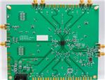
Board Information
OSCin
By default the board is configured to use the on-board crystal oscillator. It is also possible to use the
board with a single ended or differential reference source at the OSCin port. Below are several
possible configurations for driving OSCin.
OSCin using on board crystal oscillator [default]
0 ohm
R8, R11, R20 [power to crystal oscillator], R109
39 ohm
R9 [can also be 0 ohm – depends on oscillator output power, 39 ohms
to be a voltage divider]
51 ohm
R15
0.1 uF
C35, C36 (C5 is a 0.1 uF 0402 cap which may be moved to C36)
Open
C4, C5
R7, R10, R12, R13, R14, R16, R17, R79, R112
Differential OSCin setup
0 ohm
R7, R8, R10, R13
100 ohm
R17
0.1 uF
C5, C35 (C36 is a 0.1 uF 0402 cap which may be moved to C5)
Open
C4, C36
R11, R12, R14, R15, R16, R79
R20 [remove power from crystal oscillator for noise reasons]
Single ended OSCin setup
0 ohm
R7, R8
51 ohm
R15
0.1 uF
C35, C36 (C5 is a 0.1 uF 0402 cap which may be moved to C36)
Open
C4, C5
R10, R11, R12, R13, R14, R16, R17, R79
R20 [remove power from crystal oscillator for noise reasons]
Fout
Fout allows direct access to the internal VCO before the clock distribution section. The EN_Fout bit
must be selected to enable Fout. A 3 dB pad is placed on R80, R81, and R82.
Loop Filter
R22 and R5 form a “resistor switch” which allows either one of two different loop filters to be
selected.
Loop Filter
Resistor
Switch
Loop Filter
Components
Default Loop
Bandwidth
Loop Filter #1
[default]
R22 Shorted
C1, C2, C2p, R2
105 kHz
Loop Filter #2
R5 Shorted
C1_AUX, C2_AUX,
C2p_AUX, R2_AUX
55 Hz
8
�L M K 0 3 0 0 2 C
E V A L U A T I O N
B O A R D
O P E R A T I N G
I N S T R U C T I O N S
Features of the board
•
•
•
•
•
•
•
•
Either one of two loop filters can be selected by shorting either R22 or R5. More info
about each loop filter can be found in the General Description and Appendix A.
Test points for each of the uWire lines are scattered in the lower left corner of the board
and include: GOE_TP, DATAuWire, CLKuWire, LEuWire, SYNC_TP, and LD_TP.
Ground is located on the unstuffed 10 pin header on the left side of the board.
Ground is located on the GND_tp2 in the upper left corner of the board and GND_tp1
located to the right of the Vcc SMA connector.
Ground is located on the bottom side of the board on each pad of the unstuffed 10 pin
header GND_J2.
Vcc is located on the unstuffed 10 pin header on the upper left side of the board.
Vcc is located on VccPlane test point located to the right of the Vcc SMA.
Vcc is located on the bottom side of the board on each pad of the unstuffed 10 pin
header VCC_J2
Other Important Notes
•
•
•
•
When changing the OSCin frequency, the OSCin frequency register needs to be changed
to match.
Toggle the SYNC* pin to synchronize the clock outputs when in divided mode.
For both loop filters, a helper silkscreen is offset from the loop filters to help identify the
components according to National Semiconductor’s traditional reference designators
associated with loop filters.
The LMK0300xC PCB works for many LMK0300xC devices. Because of this the
silkscreen on the board is different from actual clock outputs in the datasheet and in
CodeLoader. Refer to the table below for the correct mapping.
Datasheet / CodeLoader
CLKout0 / CLKout0*
CLKout1 / CLKout1*
CLKout2 / CLKout2*
CLKout3 / CLKout3*
LMK0300xC EVB PCB
CLKout4 / CLKout4*
CLKout5 / CLKout5*
CLKout6 / CLKout6*
CLKout7 / CLKout7*
9
�L M K 0 3 0 0 2 C
E V A L U A T I O N
B O A R D
O P E R A T I N G
I N S T R U C T I O N S
Recommended Equipment
Power Supply
The Power Supply should be a low noise power supply. An Agilent 6623A Triple power supply with LC
filters on the output to reduce noise was used in creating these evaluation board instructions.
Phase Noise / Spectrum Analyzer
For measuring phase noise an Agilent E5052A is recommended. An Agilent E4445A PSA Spectrum
Analyzer with the Phase Noise option is also usable although the architecture of the E5052A is superior
for phase noise measurements. At frequencies less than 100 MHz the local oscillator noise of the PSA
is too high and measurements will be of the local oscillator, not the device under test.
Oscilloscope
For measuring delay an Agilent Infiniium DSO81204A was used.
Reference Oscillator
The on board crystal oscillator will provide a low noise reference signal to the device at offsets greater
than 1 kHz.
Note: The default loop filter has a loop bandwidth of ~105 kHz. Inside the loop bandwidth of a PLL the
noise is greatly affected by any noise on the reference oscillator (OSCin). Therefore any noise on the
oscillator less than ~105 kHz will be passed through and seen on the outputs. For this reason the main
output of a Signal Generator is not recommended for driving OSCin in this setup.
10
�11
Below ~1 kHz phase noise is dominated by the crystal
10 Hz – 20 MHz integrated RMS jitter = 474 fs
100 Hz – 20 MHz integrated RMS jitter = 202 fs
12 kHz – 20 MHz integrated RMS jitter = 188 fs (shown)
O P E R A T I N G
Below ~1 kHz phase noise is dominated by the crystal
10 Hz – 20 MHz integrated RMS jitter = 636 fs
100 Hz – 20 MHz integrated RMS jitter = 205 fs
12 kHz – 20 MHz integrated RMS jitter = 193 fs (shown)
B O A R D
Reference source is on board 16 MHz crystal
Output Frequency = 1632 MHz
Internal VCO, Fout output
E V A L U A T I O N
Reference source is on board 16 MHz crystal
LVPECL output CLKout0 (Labeled CLKout4 on EVB)
VCO Frequency = 1632 MHz, VCO_DIV=2, CLKout0_div=4
LVPECL output (204 MHz)
L M K 0 3 0 0 2 C
I N S T R U C T I O N S
Phase Noise
�L M K 0 3 0 0 2 C
E V A L U A T I O N
B O A R D
O P E R A T I N G
I N S T R U C T I O N S
Delays
These delay measurements illustrate how skew errors due to different length traces may be tuned out.
The delay may be adjusted in steps of 150 ps.
Delays 150, 300, 450, 600, 750
CLKout0_DLY = 0 ps
CLKout1_DLY = all delays
programmed: 0, 150, 300, 450,
600, 750, 900, 1050, 1200,
1350, 1500, 1650, 1800, 1950,
2100, and 2250 ps
12
�L M K 0 3 0 0 2 C
E V A L U A T I O N
B O A R D
O P E R A T I N G
I N S T R U C T I O N S
CodeLoader Settings
The Port Setup tab tells CodeLoader what signals are assigned to which pins. If this is wrong,
the part will not program.
Part setup can be restored to the default state by clicking Mode � “16 MHz OSCin” The default
reference oscillator used for these instructions is 16 MHz and the restored mode expects a 16
MHz OSCin signal. For the loaded mode to take affect the device must be loaded by
pressing Ctrl+L.
13
�L M K 0 3 0 0 2 C
E V A L U A T I O N
B O A R D
O P E R A T I N G
I N S T R U C T I O N S
The Bits/Pins tab shows some of the internal registers which are not accessible from any of the
other visual tabs like “PLL” and “Clock Outputs.” Right click on any of the bits for description.
Program Bits
POWERDOWN
EN_Fout
OSCin_FREQ
PLL_MUX
DIV4
RESET
VCO_R3_LF
VCO_R4_LF
VCO_C3_C4_LF
EN_CLKout0..3
EN_CLKout_Global
Powers the part down.
Turns on the Fout pin for measuring the internal VCO.
Must be set to the OSCin frequency in MHz.
Programmable to many different values to support Lock Detect or aid
troubleshooting.
Shall be checked for OSCin frequencies greater than 20 MHz.
The registers can be defaulted by checking and unchecking RESET.
Software bits will not reflect this.
Internal loop filter values, also accessible from Clock Outputs tab.
Enable CLKout bits from CLKout0 to CLKout7. Also accessible from Clock
Outputs tab.
Enable all clock outs. If unselected then the EN_CLKouts are overridden
and the outputs are all disabled.
Program Pins
GOE
SYNC*
TRIGGER
Set Global Output Enable to high or low logic level. GOE is not used.
See Board Information section for usage of this pin.
Set SYNC* pin to high or low logic level.
Set auxiliary trigger pin to high or low logic level.
14
�L M K 0 3 0 0 2 C
E V A L U A T I O N
B O A R D
O P E R A T I N G
I N S T R U C T I O N S
The Registers tab shows the raw bits which will be programmed when device is loaded by
clicking Keyboard Controls � Load Device or Ctrl+L.
The Clock Outputs tab allows the user to visualize the clock distribution portions of the device.
From this tab the device’s dividers, delays, clock output muxes, and output drivers can be
programmed along with internal loop filter values. The PLL block shows the R and N divider
values however to change these values either click on the PLL tab or the blue PLL box to access
the PLL tab to make changes to the PLL.
15
�L M K 0 3 0 0 2 C
E V A L U A T I O N
B O A R D
O P E R A T I N G
I N S T R U C T I O N S
The PLL tab shows a conventional PLL diagram along with the VCO Divider. It is important to
realize that the total effective N value is PLL N Counter * VCO Divider. This means that the
“channel spacing” is the Phase Detector Frequency * VCO Divider. Depending on the
situation, this may require the R Counter multiplied up by the value of the VCO Divider to achieve
desired VCO output frequencies.
Example: If the desired VCO output frequency was 1648 MHz, R would need to be increased to
2 before 1648 MHz could be programmed because of the VCO Divider of 2 would only allow
programming of 1600, 1632, 1664, etc. with a 16 MHz phase detector frequency – because
changing the N counter from 51 to 52 changes to total N by two, 102 to 104!
16
�L M K 0 3 0 0 2 C
E V A L U A T I O N
B O A R D
O P E R A T I N G
I N S T R U C T I O N S
Appendix A: VCO Performance
The internal VCO performance is measured by using a narrow bandwidth loop filter. By default
the narrow loop bandwidth filter is stuffed as Loop Filter #2 in positions C1_AUX, C2_AUX,
C2p_AUX, and R2_AUX and has a loop bandwidth of 55 Hz.
See the Loop Filter section in Board Options for more detail about switching between the two
different loop filters.
Loop Filter #2
55 Hz
Kφ
φ
Fcomp
500 kHz
Crystal Frequency
16 MHz
Output Frequency
1566 to 1724 MHz
Supply Voltage
3.3 Volts
VCO Gain
13 MHz/Volt
Phase Margin
58º
Loop Bandwidth
100 uA
Charge Pump
R3
600 Ω
R4
200 Ω
VCO
C2
10 uF
C3
150 pF
C4
110 pF
R2
820 Ω
C1
820 nF
CPout
This loop filter is located on the top side of the PCB and is selected by placing a
0 ohm resistor on pad R5.
This loop filter has been designed with a very small loop bandwidth to minimize
the PLL from interacting with the noise of the VCO to permit a VCO phase noise
measurement.
17
�L M K 0 3 0 0 2 C
E V A L U A T I O N
B O A R D
O P E R A T I N G
I N S T R U C T I O N S
VCO Phase Noise – Narrow Loop Bandwidth
This plot shows the noise of the VCO at 1632 MHz using a 500 kHz Phase
Detector Frequency. An external oscillator was used for this plot, since the VCO
noise dominates, reference oscillator noise is not critical.
The loop bandwidth has been minimized so that the VCO is the dominant noise
contributor.
10 Hz – 20 MHz integrated RMS jitter = 107.6 ps
100 Hz – 20 MHz integrated RMS jitter = 28.1 ps (shown)
1 kHz – 20 MHz integrated RMS jitter = 2.7 ps
12 kHz – 20 MHz integrated RMS jitter = 0.303 ps
18
�L M K 0 3 0 0 2 C
E V A L U A T I O N
B O A R D
O P E R A T I N G
I N S T R U C T I O N S
Appendix B: Impact of Reference on Phase Noise
Inside the loop bandwidth of a PLL the phase noise is set by the quality of the
reference oscillator used. For this reason it is important to select a reference
oscillator suitable for the application.
Test Setup
Using the same loop filter as described in the General Description and by driving
the OSCin frequency with an ultra low jitter 100 MHz Wetzel Crystal (50104517D) and setting R = 5 to achieve a phase detector frequency of 20 MHz. A
very low integrated RMS jitter of 201 fs is measured vs. the 474 fs measured in
the Phase Noise section with 16 MHz crystal in the bandwidth of 10 Hz to 20
MHz.
10 Hz – 20 MHz integrated RMS jitter = 201 fs (shown)
100 Hz – 20 MHz integrated RMS jitter = 197 fs
1 kHz – 20 MHz integrated RMS jitter = 196 fs
12 kHz – 20 MHz integrated RMS jitter = 188 fs
Conclusion
This diagram illustrates how the phase noise inside the loop bandwidth is set by
the quality of the reference oscillator used. Phase noise outside the loop
bandwidth is set by the VCO noise level.
19
�L M K 0 3 0 0 2 C
E V A L U A T I O N
B O A R D
O P E R A T I N G
I N S T R U C T I O N S
Appendix C: Schematics
LMK0300x - Main Board
LMK0300x - Main Board.sch
LMK0300x - Outputs
LMK0300x - Outputs.sch
F1
PCB_LMK0300x
Vcc
Vcc
J2
1
3
5
7
9
J3
2
4
6
8
10
1
3
5
7
9
GND_HDR
2
4
6
8
10
VCC_HDR
Vcc
Vcc
J4
1
3
5
7
9
J5
2
4
6
8
10
1
3
5
7
9
GND_HDR
2
4
6
8
10
VCC_HDR
20
�L M K 0 3 0 0 2 C
E V A L U A T I O N
B O A R D
O P E R A T I N G
I N S T R U C T I O N S
R109
SMA
TCXO_RF
Vin
R3
Vcc
0 ohm
Vcc
R110
Open
0 ohm
Vcc
OSCin
R111
Open
C3
Open
R14
Open
R11
0 ohm
GND
Vcc
B1
1
2
3
R10
Open
R12
0 ohm
6
5
4
Sd
S-ct
S
R17
Open
0 ohm
Osc1
C9
0.1 uF
Y1
0.1 uF
Osc 33xx
1
C5
2
DUT_OSCin*
Open
C6
Open
Open
R13
SMA
OSCin*
R18
Open
DUT_OSCin
ADT2-1T
P
NC
Pd
R20
C7
Open
Vcc
C35
0 ohm
R7
Open
SMA
OSCin
R16
Open
R8
GND
R112
Open
Open
R15
51 ohm
R79
Open
C4
C36
Open
0.1 uF
CE/NC
Vdd
GND
OUT
4
R9
3
39 ohm
OSC - CRYSTEK 33XX
TCXO_RF
Vin
GND_tp1
R1
0 ohm
GND_tp2
Vcc
C20
100 pF
Vcc3
C26
100 pF
Vcc4
C27
100 pF
Vcc5
C28
100 pF
Vcc6
R19
Open
2
C19
10 uF
C78
10 uF
12
38
37
Vcc11
CLKout4
CLKout4*
41
40
39
Vcc12
CLKout5
44
43
42
Vcc13
CLKout6
CLKout5*
47
46
45
CLKout6*
Vcc14
OSCin*
LDObyp1
OSCin
LDObyp2
SYNC*
GOE
Vcc7
LD
GND
C38
0.1 uF
Vcc
Vcc
Vcc
C13
Open
R84
27 k
R89
15 k
CLKout1
CLKout1*
LEuWire
C14
Open
Vcc
0 ohm
31
Vcc
29
C1
Open
DUT_OSCin*
28
LD
R85
27 k
R90
15 k
R91
15 k
R25
Open
R6
C15
Open
0 ohm
Vcc
SYNC*
26
25
SYNC*_TP
C2_AUX
Open
C1_AUX
820 nF
Vcc
CLKout2*
CLKout2
Vcc
Pin10_TP
GOE
uWire
HEADER_2X5(POLARIZED)
C73
1 uF
C37
0.1 uF
C70
1 uF
C39
0.1 uF
C80
1 uF
C40
0.1 uF
C71
1 uF
C41
0.1 uF
C81
1 uF
C42
0.1 uF
C72
1 uF
C43
0.1 uF
C82
1 uF
C44
0.1 uF
C83
1 uF
C45
0.1 uF
C74
1 uF
C46
0.1 uF
C84
1 uF
C47
0.1 uF
C75
1 uF
C48
0.1 uF
C85
1 uF
C49
0.1 uF
C76
1 uF
C50
0.1 uF
C77
1 uF
C51
0.1 uF
R92
180 ohm
1
3
5
7
9
D1
3.3 V zener
R27
Open
C79
1 uF
Vcc
2
4
6
8
10
GOE
OpenSMA
R30
2.2 k
Pin7_TP
Vcc
Pin5_TP
R29
2.2 k
SYNC*
OpenSMA
R93
180 ohm
R28
SYNC*
Open
C34
100 pF
D2
3.3 V zener
21
C2p
Open
R2
1.8 k
DUT_OSCin
27
LD
OpenSMA
Vcc
C2
12 nF
Open
R5
30
R24
Open
LEuWire
CLKuWire
R88
15 k
R22
32
CLKout3*
CLKout3
Vcc
R83
27 k
Vcc
33
LD_TP
CLKout0
CLKout0*
DATAuWire
34
CLKout3*
R26
Open
Vcc10
Vcc2
CLKout3
LD
Vcc8
Vcc6
11
Vcc9
LMK0300XC
NC
36
35
24
GOE
R95
0 ohm
LEuWire
23
9
10
R94
0 ohm
CPout
CLKout2*
Vcc14
Vcc9
Vcc10
DATAuWire
CLKout2
C33
100 pF
8
CLKuWire
22
Vcc13
NC
21
C31
100 pF
Vcc
NC
20
7
Bias
Vcc5
6
LEuWire
C69
1 uF
Vcc1
CLKout1*
5
DATAuWire
Open
U1
Fout
CLKout1
4
CLKuWire
Fout*
OpenSMA
Vcc8
DATAuWire
OUT
R104
0 ohm
GND
19
R81
270 ohm
3
18
R80
270 ohm
47 pF
17
2
Vcc
18 ohm
Open
Vcc12
C68
R82
1
2
3
Vcc4
Pd
NC
P
16
1
ADTL2-18
CLKout7
CLKout7*
48
Sd
NC
S
GND
Vcc7
B2
6
5
4
GOE_TP
CLKuWire
Vdd
GND
Vcc
0
SMA
13
C32
100 pF
Fout
CLKout0*
C25
100 pF
Vcc11
CLKout0
0 ohm
Vcc3
C86
Open
R4
Vcc2
C30
100 pF
C24
100 pF
Vcc
NC
Open
R105
C29
100 pF
C23
100 pF
Vcc
Vcc1
15
C22
100 pF
CLKout4*
CLKout4
Vcc
C11
Open
Vcc
CLKout5*
CLKout5
CLKout7
CLKout7*
14
C21
100 pF
C17
10 uF
CLKout6
CLKout6*
Osc2
C10
Open
Y2
Osc CCHD-950
1
C18
10 uF
Open
C8
Open
Vcc
C16
10 uF
C12
Open
R21
GND
VccPlane
Vcc
R2_AUX
820 ohm
C2p_AUX
10 uF
4
3
R23
Open
TCXO_RF
�L M K 0 3 0 0 2 C
Vcc
E V A L U A T I O N
Vcc
Vcc
CLKout0
R35
Open
I N S T R U C T I O N S
Vcc
Vcc
CLKout2
R40
Open
C52
CLKout0
OpenSMA
PC1
PC2
B3
C53
CLKout0*
SMA
CLKout0*
0.1 uF
PC3
PC4
C55
0.1 uF
C57
R36
Open
R38
Open
R39
Open
Open
6
5
4
Sd
S-ct
S
P
Pd
1
R87
0 ohm
3
ADT2-1T
GND
CLKout2*
CLKout2*
SMA
GND
0.1 uF
R34
Open
R107
R51
Open
PC5
CLKout1*
OpenSMA
CLKout1*
CLKout2
OpenSMA
CLKout2
R44
Open
0.1 uF
R41
Open
R43
Open
R45
Open
R46
Open
R108
R48
Open
Open
Vcc
Vcc
Vcc
CLKout3
R56
Open
CLKout3
R61
Open
CLKout4
PC7
PC8
C59
PC10
C61
R63
Open
R55
Open
Vcc
R57
Open
R96
120 ohm
R97
120 ohm
R98
120 ohm
Vcc
CLKout7
R74
Open
R76
Open
C66
CLKout7
SMA
CLKout7
0.1 uF
PC15
PC16
C67
R78
Open
CLKout7*
SMA
CLKout7*
0.1 uF
R102
120 ohm
R103
120 ohm
PC12
C63
R62
Open
R75
Open
R77
Open
22
R99
120 ohm
CLKout6
OpenSMA
CLKout6
R68
Open
PC13
CLKout5*
OpenSMA
PC14
C65
0.1 uF
R65
Open
R67
Open
R100
120 ohm
R101
120 ohm
R73
Open
CLKout6*
OpenSMA
CLKout6*
0.1 uF
R60
Open
R71
Open
0.1 uF
CLKout5*
0.1 uF
Vcc
C64
OpenSMA
PC11
CLKout4*
SMA
CLKout4*
0.1 uF
CLKout5
0.1 uF
PC9
CLKout3*
OpenSMA
CLKout3*
R69
Open
CLKout5
0.1 uF
R58
Open
Vcc
R66
Open
C62
SMA
CLKout4
0.1 uF
Vcc
R50
Open
CLKout6
R64
Open
C60
OpenSMA
CLKout3
R53
120 ohm
Vcc
CLKout5
R59
Open
C58
R52
120 ohm
Vcc
CLKout4
R54
Open
R49
Open
Open
R86
C56
0.1 uF
R37
Open
Vcc
R47
Open
Open
CLKout1
CLKout1
0.1 uF
R106
R42
Open
C54
SMA
CLKout0
R32
Open
O P E R A T I N G
CLKout1
R33
Open
R31
Open
B O A R D
R70
Open
R72
Open
�L M K 0 3 0 0 2 C
E V A L U A T I O N
B O A R D
O P E R A T I N G
I N S T R U C T I O N S
Appendix D: Bill of Materials
Part
Capacitors
47 pF
Manufacturer
Part Number
Qnt
Kemet
C0603C470J5GAC
1
100 pF
100 pF
12 nF
Kemet
Kemet
Kemet
C0402C101J5GAC
C0603C101J5GAC
C0603C123K1RACTU
14
1
1
0.1 uF
Kemet
C0603C104J3RAC
16
0.1 uF
820 nF
Kemet
Kemet
C0402C104J4RAC
C0603C824K8PAC
18
1
1 uF
10 uF
10 uF
Kemet
Kemet
Kemet
C0603C105K8VAC
C0805C106K9PAC
C0805C106K9PAC
16
5
1
Resistors
0 ohm
0 ohm
0 ohm
18 ohm
39 ohm
51 ohm
Vishay
Yageo
Vishay
Vishay
Vishay
Vishay/Dale
CRCW0603000ZRT1
RC0805JR-070RL
CRCW0603000ZRT1
CRCW0603180JRT1
CRCW0603390JRT1
CRCW060351R0JNEA
10
2
2
1
1
1
120 ohm
180 ohm
270 ohm
820 ohm
1.8 k
2.2 k
Vishay
Vishay
Vishay
Vishay
Vishay/Dale
Vishay/Dale
CRCW0402120RJNED
CRCW0603181JRT1
CRCW0603271JRT1
CRCW0603821JRT1
CRCW06031K80JNEA
CRCW06032K20JNEA
10
2
2
1
1
2
23
Identifier
C68
C20, C21, C22, C23, C24, C25, C26, C27, C28, C29,
C30, C31, C32, C33
C34
C2
C9, C37, C38, C39, C40, C41, C42, C43, C44, C45,
C46, C47, C48, C49, C50, C51
C35, C36, C52, C53, C54, C55, C56, C57, C58, C59,
C60, C61, C62, C63, C64, C65, C66, C67
C1_AUX
C69, C70, C71, C72, C73, C74, C75, C76, C77, C79,
C80, C81, C82, C83, C84, C85
C2p_AUX, C16, C17, C18, C19
C78
R1, R3, R6, R11, R12, R20, R22, R95, R104, R109
R4, R8
R87, R94
R82
R9
R15
R52, R53, R96, R97, R98, R99, R100, R101, R102,
R103
R92, R93
R80, R81
R2_AUX
R2
R29, R30
�L M K 0 3 0 0 2 C
15 k
27 k
E V A L U A T I O N
B O A R D
O P E R A T I N G
I N S T R U C T I O N S
Vishay
Vishay
CRCW0603153JRT1
CRCW0603273JRT1
4
3
R88, R89, R90, R91
R83, R84, R85
LMK0300xC
OSC - CRYSTEK 33xx
ADT2-1T
National
Semiconductor
Crystek
Minicircuits
LMK03002CI
C3391-16.000
ADT2-1T
1
1
1
SMA
3.3 V zener
Johnson Components
Comchip
11
2
PCB_LMK0300x
HEADER_2X5(POLARIZED)
SPCS-8
Printed Circuits Corp
FCI Electronics
SPC Technology
142-0701-851
CZRU52C3V3
PCB_LMK0300x rev
1.1, 6-16-2007
52601-S10-8
SPCS-8
U1
Y1
B3
CLKout0, CLKout0*, CLKout2*, CLKout4, CLKout4*,
CLKout7, CLKout7*, Fout, OSCin, OSCin*, Vcc
D1, D2
1
1
4
F1
uWire
Standoffs in the four corners (insert from bottom)
Open
-
Open
2
Open
-
603
32
B1, B2
C1, C2_AUX, C6, C7, C8, C10, C11, C12, C13, C14, C15, R5, R7,
R10, R14, R16, R17, R18, R19, R21, R23, R24, R25, R26, R27,
R28, R79, R105, R107, R110, R111, R112
Open
-
805
1
C2p
Open
-
Open
1
Open
-
402
16
Open
-
603
34
OpenSMA
-
Open
13
C3
C4, C5, R31, R32, R37, R38, R39, R44, R45, R46, R51, R58, R63,
R68, R73, R78
C86, R33, R34, R35, R36, R40, R41, R42, R43, R47, R48, R49,
R50, R54, R55, R56, R57, R59, R60, R61, R62, R64, R65, R66,
R67, R69, R70, R71, R72, R74, R75, R76, R77, R86
CLKout1, CLKout1*, CLKout2, CLKout3, CLKout3*, CLKout5,
CLKout5*, CLKout6, CLKout6*, Fout*, GOE, LD, SYNC*
Open
-
HEADER_2X5
2
J2, J4
Open
-
HEADER_2X5
2
J3, J5
Open
-
805
3
R13, R106, R108
Open
-
Open
1
Y2
Other
Open
24
�L M K 0 3 0 0 2 C
E V A L U A T I O N
B O A R D
O P E R A T I N G
Appendix E: Build Diagram
25
I N S T R U C T I O N S
�L M K 0 3 0 0 2 C
E V A L U A T I O N
B O A R D
O P E R A T I N G
I N S T R U C T I O N S
Bottom Build Diagram
26
�IMPORTANT NOTICE
Texas Instruments Incorporated and its subsidiaries (TI) reserve the right to make corrections, modifications, enhancements, improvements,
and other changes to its products and services at any time and to discontinue any product or service without notice. Customers should
obtain the latest relevant information before placing orders and should verify that such information is current and complete. All products are
sold subject to TI’s terms and conditions of sale supplied at the time of order acknowledgment.
TI warrants performance of its hardware products to the specifications applicable at the time of sale in accordance with TI’s standard
warranty. Testing and other quality control techniques are used to the extent TI deems necessary to support this warranty. Except where
mandated by government requirements, testing of all parameters of each product is not necessarily performed.
TI assumes no liability for applications assistance or customer product design. Customers are responsible for their products and
applications using TI components. To minimize the risks associated with customer products and applications, customers should provide
adequate design and operating safeguards.
TI does not warrant or represent that any license, either express or implied, is granted under any TI patent right, copyright, mask work right,
or other TI intellectual property right relating to any combination, machine, or process in which TI products or services are used. Information
published by TI regarding third-party products or services does not constitute a license from TI to use such products or services or a
warranty or endorsement thereof. Use of such information may require a license from a third party under the patents or other intellectual
property of the third party, or a license from TI under the patents or other intellectual property of TI.
Reproduction of TI information in TI data books or data sheets is permissible only if reproduction is without alteration and is accompanied
by all associated warranties, conditions, limitations, and notices. Reproduction of this information with alteration is an unfair and deceptive
business practice. TI is not responsible or liable for such altered documentation. Information of third parties may be subject to additional
restrictions.
Resale of TI products or services with statements different from or beyond the parameters stated by TI for that product or service voids all
express and any implied warranties for the associated TI product or service and is an unfair and deceptive business practice. TI is not
responsible or liable for any such statements.
TI products are not authorized for use in safety-critical applications (such as life support) where a failure of the TI product would reasonably
be expected to cause severe personal injury or death, unless officers of the parties have executed an agreement specifically governing
such use. Buyers represent that they have all necessary expertise in the safety and regulatory ramifications of their applications, and
acknowledge and agree that they are solely responsible for all legal, regulatory and safety-related requirements concerning their products
and any use of TI products in such safety-critical applications, notwithstanding any applications-related information or support that may be
provided by TI. Further, Buyers must fully indemnify TI and its representatives against any damages arising out of the use of TI products in
such safety-critical applications.
TI products are neither designed nor intended for use in military/aerospace applications or environments unless the TI products are
specifically designated by TI as military-grade or "enhanced plastic." Only products designated by TI as military-grade meet military
specifications. Buyers acknowledge and agree that any such use of TI products which TI has not designated as military-grade is solely at
the Buyer's risk, and that they are solely responsible for compliance with all legal and regulatory requirements in connection with such use.
TI products are neither designed nor intended for use in automotive applications or environments unless the specific TI products are
designated by TI as compliant with ISO/TS 16949 requirements. Buyers acknowledge and agree that, if they use any non-designated
products in automotive applications, TI will not be responsible for any failure to meet such requirements.
Following are URLs where you can obtain information on other Texas Instruments products and application solutions:
Products
Applications
Audio
www.ti.com/audio
Automotive and Transportation www.ti.com/automotive
Amplifiers
amplifier.ti.com
Communications and Telecom www.ti.com/communications
Data Converters
dataconverter.ti.com
Computers and Peripherals
www.ti.com/computers
DLP® Products
www.dlp.com
Consumer Electronics
www.ti.com/consumer-apps
DSP
dsp.ti.com
Energy and Lighting
www.ti.com/energy
Clocks and Timers
www.ti.com/clocks
Industrial
www.ti.com/industrial
Interface
interface.ti.com
Medical
www.ti.com/medical
Logic
logic.ti.com
Security
www.ti.com/security
Power Mgmt
power.ti.com
Space, Avionics and Defense
www.ti.com/space-avionics-defense
Microcontrollers
microcontroller.ti.com
Video and Imaging
www.ti.com/video
RFID
www.ti-rfid.com
OMAP Mobile Processors
www.ti.com/omap
Wireless Connectivity
www.ti.com/wirelessconnectivity
TI E2E Community Home Page
e2e.ti.com
Mailing Address: Texas Instruments, Post Office Box 655303, Dallas, Texas 75265
Copyright © 2012, Texas Instruments Incorporated
�


 工商网监
湘ICP备2023018690号
工商网监
湘ICP备2023018690号
