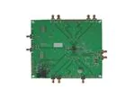
LMK030xxC Evaluation Board
User's Guide
November 2013
SNAU040A
�LMK03000C/01C/02C/33C
Precision Clock Conditioner with Integrated VCO
Evaluation Board Operating Instructions
April 2009
2
SNAU040A
LMK030xxC Evaluation Board User’s Guide
Copyright © 2013, Texas Instruments Incorporated
www.ti.com
November 2013
�TABLE OF CONTENTS
EQUIPMENT ..................................................................................................................................................................................5
BASIC OPERATION ........................................................................................................................................................................6
LMK03000C BOARD INFORMATION ............................................................................................................................................9
LOOP FILTER #1 ...........................................................................................................................................................................9
OSCin................................................................................................................................................... 10
Fout ...................................................................................................................................................... 10
Loop Filter ........................................................................................................................................... 10
Features of the board ............................................................................................................................ 11
Other Important Notes ......................................................................................................................... 11
Evaluation Board Revision v1.0 Errata ............................................................................................... 11
Results .................................................................................................................................................. 11
PHASE NOISE .............................................................................................................................................................................. 11
DELAYS ...................................................................................................................................................................................... 13
VCO PERFORMANCE .................................................................................................................................................................. 14
IMPACT OF REFERENCE ON PHASE NOISE ................................................................................................................................... 16
LMK03001C BOARD INFORMATION .......................................................................................................................................... 17
LOOP FILTER #1 ......................................................................................................................................................................... 17
OSCin................................................................................................................................................... 18
Fout ...................................................................................................................................................... 18
Loop Filter ........................................................................................................................................... 18
Features of the board ............................................................................................................................ 19
Other Important Notes ......................................................................................................................... 19
Evaluation Board Revision v1.0 Errata ............................................................................................... 19
Results .................................................................................................................................................. 19
PHASE NOISE .............................................................................................................................................................................. 19
DELAYS ...................................................................................................................................................................................... 21
VCO PERFORMANCE .................................................................................................................................................................. 22
IMPACT OF REFERENCE ON PHASE NOISE ................................................................................................................................... 24
LMK03002C BOARD INFORMATION .......................................................................................................................................... 25
LOOP FILTER #1 ......................................................................................................................................................................... 25
OSCin................................................................................................................................................... 26
Fout ...................................................................................................................................................... 26
Loop Filter ........................................................................................................................................... 26
Features of the board ............................................................................................................................ 27
Other Important Notes ......................................................................................................................... 27
Results .................................................................................................................................................. 27
PHASE NOISE .............................................................................................................................................................................. 27
DELAYS ...................................................................................................................................................................................... 29
VCO PERFORMANCE .................................................................................................................................................................. 30
Loop Filter #2 ...................................................................................................................................... 30
IMPACT OF REFERENCE ON PHASE NOISE ................................................................................................................................... 32
LMK03033C BOARD INFORMATION .......................................................................................................................................... 33
LOOP FILTER #1 ......................................................................................................................................................................... 33
OSCin................................................................................................................................................... 33
Fout ...................................................................................................................................................... 34
Loop Filter ........................................................................................................................................... 34
Features of the board ............................................................................................................................ 35
November 2013
LMK030xxC Evaluation Board User’s Guide
Copyright © 2013, Texas Instruments Incorporated
www.ti.com
SNAU040A
3
�Other Important Notes ......................................................................................................................... 35
Evaluation Board Revision v1.0 Errata ............................................................................................... 35
Results .................................................................................................................................................. 35
PHASE NOISE .............................................................................................................................................................................. 35
DELAYS ...................................................................................................................................................................................... 37
VCO PERFORMANCE .................................................................................................................................................................. 38
APPENDIX A: SCHEMATICS......................................................................................................................................................... 40
APPENDIX B: BILL OF MATERIALS ............................................................................................................................................. 43
APPENDIX C: BUILD DIAGRAM................................................................................................................................................... 45
APPENDIX D: QUICK START ON EVM COMMUNICATION .......................................................................................................... 47
4
SNAU040A
LMK030xxC Evaluation Board User’s Guide
Copyright © 2013, Texas Instruments Incorporated
www.ti.com
November 2013
�Equipment
Power Supply
The Power Supply should be a low noise power supply. An Agilent 6623A Triple power supply with LC filters on the
output to reduce noise was used in creating these evaluation board instructions.
Phase Noise / Spectrum Analyzer
For measuring phase noise an Agilent E5052A is recommended. An Agilent E4445A PSA Spectrum Analyzer with the
Phase Noise option is also usable although the architecture of the E5052A is superior for phase noise measurements. At
frequencies less than 100 MHz the local oscillator noise of the PSA is too high and measurements will be of the local
oscillator, not the device under test.
Oscilloscope
The oscilloscope and probes should be capable of measuring the output frequencies of interest when evaluating this
board. The Agilent Infiniium DSO81204A was used in creating these evaluation board instructions.
Reference Oscillator
The on board crystal oscillator will provide a low noise reference signal to the device at offsets greater than 1 kHz.
Note: The default loop filter has a loop bandwidth of ~60 kHz. Inside the loop bandwidth of a PLL the noise is greatly
affected by any noise on the reference oscillator (OSCin). Therefore any noise on the oscillator less than 60 kHz will be
passed through and seen on the outputs. For this reason the main output of a Signal Generator is not recommended for
driving OSCin in this setup.
November 2013
LMK030xxC Evaluation Board User’s Guide
Copyright © 2013, Texas Instruments Incorporated
www.ti.com
SNAU040A
5
�Basic Operation
1. Connect a low noise 3.3 V power supply to the Vcc connector located at the top left of the board.
2. Please see Appendix D for quick start on interfacing the board. Connect PC to the uWire header.
1
Power
Supply
3.0 V
Power
Power
Cable
Cable
Vcc
2
uWire
header
Please
Please see
see
Appendix
Appendix D
D for
for
interface
interface info
info
Laptop
Laptop or
or PC
PC
6
SNAU040A
LMK030xxC Evaluation Board User’s Guide
Copyright © 2013, Texas Instruments Incorporated
www.ti.com
November 2013
�3. Start CodeLoader4.exe.
4. Select the USB or LPT Communication Mode on the Port Setup tab as appropriate.
5. Enable output to be measured, any of CLKout(0-7) or EN_Fout from either Clock Outputs or Bits/Pins tab. In
example below, CLKout0 is enabled.
November 2013
LMK030xxC Evaluation Board User’s Guide
Copyright © 2013, Texas Instruments Incorporated
www.ti.com
SNAU040A
7
�Program Bits
POWERDOWN
EN_Fout
OSCin_FREQ
PLL_MUX
DIV4
RESET
VCO_R3_LF
VCO_R4_LF
VCO_C3_C4_LF
EN_CLKout0..7
EN_CLKout_Global
Program Pins
GOE
SYNC*
TRIGGER
Powers the part down.
Turns on the Fout pin for measuring the internal VCO.
Must be set to the OSCin frequency in MHz.
Programmable to many different values to support Lock Detect or aid
troubleshooting.
Shall be checked for OSCin frequencies greater than 20 MHz.
The registers can be defaulted by checking and unchecking RESET.
Software bits will not reflect this.
Internal loop filter values, also accessible from Clock Outputs tab.
Enable CLKout bits from CLKout0 to CLKout7. Also accessible from Clock
Outputs tab.
Enable all clock outs. If unselected then the EN_CLKouts are overridden
and the outputs are all disabled.
Set Global Output Enable to high or low logic level.
Set SYNC* pin to high or low logic level.
Set auxiliary trigger pin to high or low logic level.
6. Program the part by clicking “Keyboard Controls” “Load Device” OR by shortcut “Ctrl+L”.
7. Make measurements… After programming, the uWire cabling can be unplugged from the evaluation board to
minimize noise and EMI.
8
SNAU040A
LMK030xxC Evaluation Board User’s Guide
November 2013
Copyright © 2013, Texas Instruments Incorporated
www.ti.com
�LMK03000C Board information
Loop Filter #1
Phase Margin
70.0º
Loop Bandwidth
55.3 kHz
fPD
9.72 MHz
Crystal Frequency
19.44 MHz
Output Frequency
1185 to 1296 MHz
Supply Voltage
3.3 Volts
VCO Gain
8 MHz/Volt
3200 uA
Charge Pump
R3
600
R4
200
VCO
C2
12 nF
C3
150 pF
C4
110 pF
R2
1.8 k
C1
open
CPout
Loop filter #1 is selected by placing a 0 ohm resistor on pad R22.
This loop filter has been designed for optimal RMS jitter using a low noise
reference.
November 2013
LMK030xxC Evaluation Board User’s Guide
Copyright © 2013, Texas Instruments Incorporated
www.ti.com
SNAU040A
9
�OSCin
By default the board is configured to use the on-board crystal oscillator. It is also possible to use the board with a single
ended or differential reference source at the OSCin port. Below are several possible configurations for driving OSCin.
OSCin using on board crystal oscillator [default]
0 ohm
R8, R11, R20 [power to crystal oscillator], R109
39 ohm
R9 [can also be 0 ohm – depends on oscillator output power, 39 ohms
to be a voltage divider]
51 ohm
R15
0.1 uF
C35, C36 (C5 is a 0.1 uF 0402 cap which may be moved to C36)
Open
C4, C5
R7, R10, R12, R13, R14, R16, R17, R79, R112
Differential OSCin setup
0 ohm
R7, R8, R10, R13
100 ohm
R44
0.1 uF
C5, C35 (C36 is a 0.1 uF 0402 cap which may be moved to C5)
Open
C4, C36
R11, R12, R14, R15, R16, R79
R20 [remove power from crystal oscillator for noise reasons]
Single ended OSCin setup
0 ohm
R7, R8
51 ohm
R15
0.1 uF
C35, C36 (C5 is a 0.1 uF 0402 cap which may be moved to C36)
Open
C4, C5
R10, R11, R12, R13, R14, R16, R17, R79
R20 [remove power from crystal oscillator for noise reasons]
Fout
Fout allows direct access to the internal VCO before the clock distribution section. The EN_Fout bit must be selected to
enable Fout. A 3 dB pad is placed on R80, R81, and R82.
Loop Filter
R22 and R5 form a “resistor switch” which allows either one of two different loop filters to be selected.
Loop Filter
Resistor
Switch
Loop Filter
Components
Default Loop
Bandwidth
Loop Filter #1
[default]
R22 Shorted
C1, C2, C2p, R2
59.1 kHz
Loop Filter #2
R5 Shorted
C1_AUX, C2_AUX,
C2p_AUX, R2_AUX
77 Hz
10
SNAU040A
LMK030xxC Evaluation Board User’s Guide
Copyright © 2013, Texas Instruments Incorporated
www.ti.com
November 2013
�Features of the board
Either one of two loop filters can be selected by shorting either R22 or R5. More info about each loop filter
can be found in the General Description and Appendix A.
Test points for each of the uWire lines are scattered in the lower left corner of the board and include:
GOE_TP, DATAuWire, CLKuWire, LEuWire, SYNC_TP, and LD_TP.
Ground is located on the unstuffed 10 pin header on the left side of the board.
Ground is located on the GND_tp2 in the upper left corner of the board and GND_tp1 located to the right
of the Vcc SMA connector.
Ground is located on the bottom side of the board on each pad of the unstuffed 10 pin header GND_J2.
Vcc is located on the unstuffed 10 pin header on the upper left side of the board.
Vcc is located on VccPlane test point located to the right of the Vcc SMA.
Vcc is located on the bottom side of the board on each pad of the unstuffed 10 pin header VCC_J2
Other Important Notes
When changing the OSCin frequency, the OSCin frequency register needs to be changed to match.
Toggle the SYNC* pin to synchronize the clock outputs when in divided mode.
For both loop filters, a helper silkscreen is offset from the loop filters to help identify the components
according to Texas Instruments Incorporated’s traditional reference designators associated with loop filters.
Evaluation Board Revision v1.0 Errata
SYNC* is labeled on the PCB as SYNC, however the logic of SYNC* is still active low!
Results
November 2013
LMK030xxC Evaluation Board User’s Guide
Copyright © 2013, Texas Instruments Incorporated
www.ti.com
SNAU040A
Below ~1 kHz phase noise is dominated by the crystal
10 Hz – 20 MHz integrated RMS jitter = 2.1 ps
100 Hz – 20 MHz integrated RMS jitter = 287 fs
12 kHz – 20 MHz integrated RMS jitter = 236 fs
Output Frequency = 1244.16 MHz
Internal VCO, Fout output
Reference source is on board 19.44 MHz crystal
Phase Noise
11
�12
SNAU040A
LMK030xxC Evaluation Board User’s Guide
Copyright © 2013, Texas Instruments Incorporated
www.ti.com
November 2013
Output is measured with a Minicircuits ADT2-1T balun.
Reference source is on board 19.44 MHz crystal
Below ~1 kHz phase noise is dominated by the crystal
10 Hz – 20 MHz integrated RMS jitter = 1.8 ps
100 Hz – 20 MHz integrated RMS jitter = 315 fs
12 kHz – 20 MHz integrated RMS jitter = 256 fs (shown)
Below ~1 kHz phase noise is dominated by the crystal
10 Hz – 20 MHz integrated RMS jitter = 1.7 ps
100 Hz – 20 MHz integrated RMS jitter = 281 fs
12 kHz – 20 MHz integrated RMS jitter = 244 fs (shown)
LVDS output CLKout0
VCO Frequency = 1244.16 MHz, VCO_DIV=2, CLKout0_div=4
LVDS output (155.52 MHz)
Output is measured with a Minicircuits ADT2-1T balun.
Reference source is on board 19.44 MHz crystal
LVPECL output CLKout4
VCO Frequency = 1244.16 MHz, VCO_DIV=2, CLKout4_div=4
LVPECL output (155.52 MHz)
�Delays
These delay measurements illustrate how skew errors due to different length traces may be tuned out.
The delay may be adjusted in steps of 150 ps.
Delays 150, 300, 450, 600, 750
CLKout0_DLY = 0 ps
CLKout1_DLY = all delays
programmed: 0, 150, 300, 450, 600,
750, 900, 1050, 1200, 1350, 1500,
1650, 1800, 1950, 2100, and 2250 ps
November 2013
LMK030xxC Evaluation Board User’s Guide
Copyright © 2013, Texas Instruments Incorporated
www.ti.com
SNAU040A
13
�VCO Performance
The internal VCO performance is measured by using a narrow bandwidth loop filter. By default the narrow loop
bandwidth filter is stuffed as Loop Filter #2 in positions C1_AUX, C2_AUX, C2p_AUX, and R2_AUX and has a loop
bandwidth of 77 Hz.
See the Loop Filter section in Board Options for more detail about switching between the two different loop filters.
Loop Filter
Phase Margin
58.7º
Loop Bandwidth
77 Hz
fPD
1.023 MHz
Crystal Frequency
19.44 MHz
Output Frequency
1185 to 1296 MHz
Supply Voltage
3.3 Volts
VCO Gain
10 MHz/Volt
100 uA
Charge Pump
R3
600
R4
200
VCO
C2
10 uF
C3
150 pF
C4
110 pF
R2
820
C1
820 nF
CPout
This loop filter is located on the top side of the PCB and is selected by placing a
0 ohm resistor on pad R5.
This loop filter has been designed with a very small loop bandwidth to minimize
the PLL from interacting with the noise of the VCO to permit a VCO phase noise
measurement.
14
SNAU040A
LMK030xxC Evaluation Board User’s Guide
Copyright © 2013, Texas Instruments Incorporated
www.ti.com
November 2013
�VCO Phase Noise - Narrow Loop Bandwidth
This plot shows the noise of the VCO at 1240 MHz using a 1 MHz Phase
Detector Frequency. An external oscillator was used for this plot, since the VCO
noise dominates, reference oscillator noise is not critical.
The loop bandwidth has been minimized so that the VCO is the dominant noise
contributor.
10 Hz – 20 MHz integrated RMS jitter = 56.9 ps (shown)
100 Hz – 20 MHz integrated RMS jitter = 25.0 ps
12 kHz – 20 MHz integrated RMS jitter = 0.304 ps (datasheet)
November 2013
LMK030xxC Evaluation Board User’s Guide
Copyright © 2013, Texas Instruments Incorporated
www.ti.com
SNAU040A
15
�Impact of Reference on Phase Noise
Inside the loop bandwidth of a PLL the phase noise is set by the quality of the reference
oscillator used. For this reason it is important to select a reference oscillator suitable for the
application.
Test Setup
Using the same loop filter as described in the General Description and by driving the OSCin
frequency with an ultra low jitter 100 MHz Wetzel Crystal (501-04517D) and setting R = 10 to
achieve a phase detector frequency of 10 MHz. A very low integrated RMS jitter of 247 fs is
measured vs. the 2.1 ps measured in the Phase Noise section with 19.44 MHz crystal in the
bandwidth of 10 Hz to 20 MHz.
10 Hz – 20 MHz integrated RMS jitter = 247 fs (shown)
100 Hz – 20 MHz integrated RMS jitter = 243 fs
12 kHz – 20 MHz integrated RMS jitter = 222 fs
Conclusion
This diagram illustrates how the phase noise inside the loop bandwidth is set by the quality of
the reference oscillator used. Phase noise outside the loop bandwidth is set by the VCO noise
level.
16
SNAU040A
LMK030xxC Evaluation Board User’s Guide
Copyright © 2013, Texas Instruments Incorporated
www.ti.com
November 2013
�LMK03001C Board information
Loop Filter #1
Phase Margin
74.4º
Loop Bandwidth
59.1 kHz
Fcomp
12.288 MHz
Crystal Frequency
12.288 MHz
Output Frequency
1470 to 1570 MHz
Supply Voltage
3.3 Volts
VCO Gain
10 MHz/Volt
3200 uA
Charge Pump
R3
100
R4
100
VCO
C2
12 nF
C3
100 pF
C4
110 pF
R2
1.8 k
C1
open
CPout
Loop filter #1 is selected by placing a 0 ohm resistor on pad R22.
This loop filter has been designed for optimal RMS jitter using a low noise
reference.
November 2013
LMK030xxC Evaluation Board User’s Guide
Copyright © 2013, Texas Instruments Incorporated
www.ti.com
SNAU040A
17
�OSCin
By default the board is configured to use the on-board crystal oscillator. It is also possible to use the board with a single
ended or differential reference source at the OSCin port. Below are several possible configurations for driving OSCin.
OSCin using on board crystal oscillator [default]
0 ohm
R8, R11, R20 [power to crystal oscillator], R109
39 ohm
R9 [can also be 0 ohm – depends on oscillator output power, 39 ohms
to be a voltage divider]
51 ohm
R15
0.1 uF
C35, C36 (C5 is a 0.1 uF 0402 cap which may be moved to C36)
Open
C4, C5
R7, R10, R12, R13, R14, R16, R17, R79, R112
Differential OSCin setup
0 ohm
R7, R8, R10, R13
100 ohm
R44
0.1 uF
C5, C35 (C36 is a 0.1 uF 0402 cap which may be moved to C5)
Open
C4, C36
R11, R12, R14, R15, R16, R79
R20 [remove power from crystal oscillator for noise reasons]
Single ended OSCin setup
0 ohm
R7, R8
51 ohm
R15
0.1 uF
C35, C36 (C5 is a 0.1 uF 0402 cap which may be moved to C36)
Open
C4, C5
R10, R11, R12, R13, R14, R16, R17, R79
R20 [remove power from crystal oscillator for noise reasons]
Fout
Fout allows direct access to the internal VCO before the clock distribution section. The EN_Fout bit must be selected to
enable Fout. A 3 dB pad is placed on R80, R81, and R82.
Loop Filter
R22 and R5 form a “resistor switch” which allows either one of two different loop filters to be selected.
Loop Filter
Resistor
Switch
Loop Filter
Components
Default Loop
Bandwidth
Loop Filter #1
[default]
R22 Shorted
C1, C2, C2p, R2
59.1 kHz
Loop Filter #2
R5 Shorted
C1_AUX, C2_AUX,
C2p_AUX, R2_AUX
77 Hz
18
SNAU040A
LMK030xxC Evaluation Board User’s Guide
Copyright © 2013, Texas Instruments Incorporated
www.ti.com
November 2013
�Features of the board
Either one of two loop filters can be selected by shorting either R22 or R5. More info about each loop filter
can be found in the General Description and Appendix A.
Test points for each of the uWire lines are scattered in the lower left corner of the board and include:
GOE_TP, DATAuWire, CLKuWire, LEuWire, SYNC_TP, and LD_TP.
Ground is located on the unstuffed 10 pin header on the left side of the board.
Ground is located on the GND_tp2 in the upper left corner of the board and GND_tp1 located to the right
of the Vcc SMA connector.
Ground is located on the bottom side of the board on each pad of the unstuffed 10 pin header GND_J2.
Vcc is located on the unstuffed 10 pin header on the upper left side of the board.
Vcc is located on VccPlane test point located to the right of the Vcc SMA.
Vcc is located on the bottom side of the board on each pad of the unstuffed 10 pin header VCC_J2
Other Important Notes
When changing the OSCin frequency, the OSCin frequency register needs to be changed to match.
Toggle the SYNC* pin to synchronize the clock outputs when in divided mode.
For both loop filters, a helper silkscreen is offset from the loop filters to help identify the components
according to Texas Instruments Incorporated’s traditional reference designators associated with loop filters.
Evaluation Board Revision v1.0 Errata
SYNC* is labeled on the PCB as SYNC, however the logic of SYNC* is still active low!
Results
November 2013
LMK030xxC Evaluation Board User’s Guide
Copyright © 2013, Texas Instruments Incorporated
www.ti.com
SNAU040A
Below ~1 kHz phase noise is dominated by the crystal
10 Hz – 20 MHz integrated RMS jitter = 782 fs
100 Hz – 20 MHz integrated RMS jitter = 269 fs
12 kHz – 20 MHz integrated RMS jitter = 238 fs
Output Frequency = 1499.136 MHz
Internal VCO, Fout output
Reference source is on board 12.288 MHz crystal
Phase Noise
19
�20
SNAU040A
LMK030xxC Evaluation Board User’s Guide
Copyright © 2013, Texas Instruments Incorporated
www.ti.com
November 2013
Output is measured with a Minicircuits ADT2-1T balun.
Reference source is on board 12.288 MHz crystal
Below ~1 kHz phase noise is dominated by the crystal
10 Hz – 20 MHz integrated RMS jitter = 702 fs
100 Hz – 20 MHz integrated RMS jitter = 277 fs
12 kHz – 20 MHz integrated RMS jitter = 245 fs (shown)
Below ~1 kHz phase noise is dominated by the crystal
10 Hz – 20 MHz integrated RMS jitter = 679 fs
100 Hz – 20 MHz integrated RMS jitter = 278 fs
12 kHz – 20 MHz integrated RMS jitter = 248 fs (shown)
LVDS output CLKout0
VCO Frequency = 1499.136 MHz, INPUT_DIV=2, CLKout0_div=4
LVDS output (187.392 MHz)
Output is measured with a Minicircuits ADT2-1T balun.
Reference source is on board 12.288 MHz crystal
LVPECL output CLKout4
VCO Frequency = 1499.136 MHz, INPUT_DIV=2, CLKout4_div=4
LVPECL output (187.392 MHz)
�Delays
These delay measurements illustrate how skew errors due to different length traces may be tuned out.
The delay may be adjusted in steps of 150 ps.
Delays 150, 300, 450, 600, 750
CLKout0_DLY = 0 ps
CLKout1_DLY = all delays
programmed: 0, 150, 300, 450, 600,
750, 900, 1050, 1200, 1350, 1500,
1650, 1800, 1950, 2100, and 2250 ps
November 2013
LMK030xxC Evaluation Board User’s Guide
Copyright © 2013, Texas Instruments Incorporated
www.ti.com
SNAU040A
21
�VCO Performance
The internal VCO performance is measured by using a narrow bandwidth loop filter. By default the narrow loop
bandwidth filter is stuffed as Loop Filter #2 in positions C1_AUX, C2_AUX, C2p_AUX, and R2_AUX and has a loop
bandwidth of 77 Hz.
See the Loop Filter section in Board Options for more detail about switching between the two different loop filters.
Loop Filter
Phase Margin
58.7º
Loop Bandwidth
77 Hz
Fcomp
1.024 MHz
Crystal Frequency
12.288 MHz
Output Frequency
1470 to 1570 MHz
Supply Voltage
3.3 Volts
VCO Gain
10 MHz/Volt
100 uA
Charge Pump
R3
600
R4
200
VCO
C2
10 uF
C3
150 pF
C4
110 pF
R2
820
C1
820 nF
CPout
This loop filter is located on the top side of the PCB and is selected by placing a
0 ohm resistor on pad R5.
This loop filter has been designed with a very small loop bandwidth to minimize
the PLL from interacting with the noise of the VCO to permit a VCO phase noise
measurement.
22
SNAU040A
LMK030xxC Evaluation Board User’s Guide
Copyright © 2013, Texas Instruments Incorporated
www.ti.com
November 2013
�VCO Phase Noise - Narrow Loop Bandwidth
This plot shows the noise of the VCO at 1500 MHz using a 1 MHz Phase
Detector Frequency. An external oscillator was used for this plot, since the VCO
noise dominates, reference oscillator noise is not critical.
The loop bandwidth has been minimized so that the VCO is the dominant noise
contributor.
10 Hz – 20 MHz integrated RMS jitter = 53.1 ps (shown)
100 Hz – 20 MHz integrated RMS jitter = 26.3 ps
12 kHz – 20 MHz integrated RMS jitter = 0.310 ps
November 2013
LMK030xxC Evaluation Board User’s Guide
Copyright © 2013, Texas Instruments Incorporated
www.ti.com
SNAU040A
23
�Impact of Reference on Phase Noise
Inside the loop bandwidth of a PLL the phase noise is set by the quality of the reference
oscillator used. For this reason it is important to select a reference oscillator suitable for the
application.
Test Setup
Using the same loop filter as described in the General Description and by driving the OSCin
frequency with an ultra low jitter 100 MHz Wetzel Crystal (501-04517D) and setting R = 10 to
achieve a phase detector frequency of 10 MHz. A very low integrated RMS jitter of 243 fs is
measured vs. the 782 fs measured in the Phase Noise section with 12.288 MHz crystal in the
bandwidth of 10 Hz to 20 MHz.
10 Hz – 20 MHz integrated RMS jitter = 243 fs (shown)
100 Hz – 20 MHz integrated RMS jitter = 240 fs
12 kHz – 20 MHz integrated RMS jitter = 220 fs
Conclusion
This diagram illustrates how the phase noise inside the loop bandwidth is set by the quality of
the reference oscillator used. Phase noise outside the loop bandwidth is set by the VCO noise
level.
24
SNAU040A
LMK030xxC Evaluation Board User’s Guide
Copyright © 2013, Texas Instruments Incorporated
www.ti.com
November 2013
�LMK03002C Board information
Loop Filter #1
Phase Margin
63º
Loop Bandwidth
105 kHz
Fcomp
16 MHz
Crystal Frequency
16 MHz
Output Frequency
1566 to 1724 MHz
Supply Voltage
3.3 Volts
VCO Gain
13 MHz/Volt
3200 uA
Charge Pump
R3
600
R4
200
VCO
C2
12 nF
C3
100 pF
C4
110 pF
R2
1.8 k
C1
open
CPout
(Loop filter #1 is selected by placing a 0 ohm resistor on pad R22)
November 2013
LMK030xxC Evaluation Board User’s Guide
Copyright © 2013, Texas Instruments Incorporated
www.ti.com
SNAU040A
25
�OSCin
By default the board is configured to use the on-board crystal oscillator. It is also possible to use the board with a single
ended or differential reference source at the OSCin port. Below are several possible configurations for driving OSCin.
OSCin using on board crystal oscillator [default]
0 ohm
R8, R11, R20 [power to crystal oscillator], R109
39 ohm
R9 [can also be 0 ohm – depends on oscillator output power, 39 ohms
to be a voltage divider]
51 ohm
R15
0.1 uF
C35, C36 (C5 is a 0.1 uF 0402 cap which may be moved to C36)
Open
C4, C5
R7, R10, R12, R13, R14, R16, R17, R79, R112
Differential OSCin setup
0 ohm
R7, R8, R10, R13
100 ohm
R17
0.1 uF
C5, C35 (C36 is a 0.1 uF 0402 cap which may be moved to C5)
Open
C4, C36
R11, R12, R14, R15, R16, R79
R20 [remove power from crystal oscillator for noise reasons]
Single ended OSCin setup
0 ohm
R7, R8
51 ohm
R15
0.1 uF
C35, C36 (C5 is a 0.1 uF 0402 cap which may be moved to C36)
Open
C4, C5
R10, R11, R12, R13, R14, R16, R17, R79
R20 [remove power from crystal oscillator for noise reasons]
Fout
Fout allows direct access to the internal VCO before the clock distribution section. The EN_Fout bit must be selected to
enable Fout. A 3 dB pad is placed on R80, R81, and R82.
Loop Filter
R22 and R5 form a “resistor switch” which allows either one of two different loop filters to be selected.
Loop Filter
Resistor
Switch
Loop Filter
Components
Default Loop
Bandwidth
Loop Filter #1
[default]
R22 Shorted
C1, C2, C2p, R2
105 kHz
Loop Filter #2
R5 Shorted
C1_AUX, C2_AUX,
C2p_AUX, R2_AUX
55 Hz
26
SNAU040A
LMK030xxC Evaluation Board User’s Guide
Copyright © 2013, Texas Instruments Incorporated
www.ti.com
November 2013
�Features of the board
Either one of two loop filters can be selected by shorting either R22 or R5. More info about each loop filter
can be found in the General Description and Appendix A.
Test points for each of the uWire lines are scattered in the lower left corner of the board and include:
GOE_TP, DATAuWire, CLKuWire, LEuWire, SYNC_TP, and LD_TP.
Ground is located on the unstuffed 10 pin header on the left side of the board.
Ground is located on the GND_tp2 in the upper left corner of the board and GND_tp1 located to the right
of the Vcc SMA connector.
Ground is located on the bottom side of the board on each pad of the unstuffed 10 pin header GND_J2.
Vcc is located on the unstuffed 10 pin header on the upper left side of the board.
Vcc is located on VccPlane test point located to the right of the Vcc SMA.
Vcc is located on the bottom side of the board on each pad of the unstuffed 10 pin header VCC_J2
Other Important Notes
When changing the OSCin frequency, the OSCin frequency register needs to be changed to match.
Toggle the SYNC* pin to synchronize the clock outputs when in divided mode.
For both loop filters, a helper silkscreen is offset from the loop filters to help identify the components
according to Texas Instruments Incorporated’s traditional reference designators associated with loop filters.
Results
November 2013
LMK030xxC Evaluation Board User’s Guide
Copyright © 2013, Texas Instruments Incorporated
www.ti.com
SNAU040A
Below ~1 kHz phase noise is dominated by the crystal
10 Hz – 20 MHz integrated RMS jitter = 782 fs
100 Hz – 20 MHz integrated RMS jitter = 269 fs
12 kHz – 20 MHz integrated RMS jitter = 238 fs
Output Frequency = 1499.136 MHz
Internal VCO, Fout output
Reference source is on board 12.288 MHz crystal
Phase Noise
27
�28
SNAU040A
LMK030xxC Evaluation Board User’s Guide
Copyright © 2013, Texas Instruments Incorporated
www.ti.com
November 2013
Output is measured with a Minicircuits ADT2-1T balun.
Reference source is on board 12.288 MHz crystal
Below ~1 kHz phase noise is dominated by the crystal
10 Hz – 20 MHz integrated RMS jitter = 702 fs
100 Hz – 20 MHz integrated RMS jitter = 277 fs
12 kHz – 20 MHz integrated RMS jitter = 245 fs (shown)
Below ~1 kHz phase noise is dominated by the crystal
10 Hz – 20 MHz integrated RMS jitter = 679 fs
100 Hz – 20 MHz integrated RMS jitter = 278 fs
12 kHz – 20 MHz integrated RMS jitter = 248 fs (shown)
LVDS output CLKout0
VCO Frequency = 1499.136 MHz, INPUT_DIV=2, CLKout0_div=4
LVDS output (187.392 MHz)
Output is measured with a Minicircuits ADT2-1T balun.
Reference source is on board 12.288 MHz crystal
LVPECL output CLKout4
VCO Frequency = 1499.136 MHz, INPUT_DIV=2, CLKout4_div=4
LVPECL output (187.392 MHz)
�Delays
These delay measurements illustrate how skew errors due to different length traces may be tuned out.
The delay may be adjusted in steps of 150 ps.
Delays 150, 300, 450, 600, 750
CLKout0_DLY = 0 ps
CLKout1_DLY = all delays
programmed: 0, 150, 300, 450, 600,
750, 900, 1050, 1200, 1350, 1500,
1650, 1800, 1950, 2100, and 2250 ps
November 2013
LMK030xxC Evaluation Board User’s Guide
Copyright © 2013, Texas Instruments Incorporated
www.ti.com
SNAU040A
29
�VCO Performance
The internal VCO performance is measured by using a narrow bandwidth loop filter. By default the narrow loop
bandwidth filter is stuffed as Loop Filter #2 in positions C1_AUX, C2_AUX, C2p_AUX, and R2_AUX and has a loop
bandwidth of 55 Hz.
See the Loop Filter section in Board Options for more detail about switching between the two different loop filters.
Loop Filter #2
Phase Margin
58º
Loop Bandwidth
55 Hz
Fcomp
500 kHz
Crystal Frequency
16 MHz
Output Frequency
1566 to 1724 MHz
Supply Voltage
3.3 Volts
VCO Gain
13 MHz/Volt
100 uA
Charge Pump
R3
600
R4
200
VCO
C2
10 uF
C3
150 pF
C4
110 pF
R2
820
C1
820 nF
CPout
This loop filter is located on the top side of the PCB and is selected by placing a
0 ohm resistor on pad R5.
This loop filter has been designed with a very small loop bandwidth to minimize
the PLL from interacting with the noise of the VCO to permit a VCO phase noise
measurement.
30
SNAU040A
LMK030xxC Evaluation Board User’s Guide
Copyright © 2013, Texas Instruments Incorporated
www.ti.com
November 2013
�VCO Phase Noise – Narrow Loop Bandwidth
This plot shows the noise of the VCO at 1632 MHz using a 500 kHz Phase
Detector Frequency. An external oscillator was used for this plot, since the VCO
noise dominates, reference oscillator noise is not critical.
The loop bandwidth has been minimized so that the VCO is the dominant noise
contributor.
10 Hz – 20 MHz integrated RMS jitter = 107.6 ps
100 Hz – 20 MHz integrated RMS jitter = 28.1 ps (shown)
1 kHz – 20 MHz integrated RMS jitter = 2.7 ps
12 kHz – 20 MHz integrated RMS jitter = 0.303 ps
November 2013
LMK030xxC Evaluation Board User’s Guide
Copyright © 2013, Texas Instruments Incorporated
www.ti.com
SNAU040A
31
�Impact of Reference on Phase Noise
Inside the loop bandwidth of a PLL the phase noise is set by the quality of the reference
oscillator used. For this reason it is important to select a reference oscillator suitable for the
application.
Test Setup
Using the same loop filter as described in the General Description and by driving the OSCin
frequency with an ultra low jitter 100 MHz Wetzel Crystal (501-04517D) and setting R = 5 to
achieve a phase detector frequency of 20 MHz. A very low integrated RMS jitter of 201 fs is
measured vs. the 474 fs measured in the Phase Noise section with 16 MHz crystal in the
bandwidth of 10 Hz to 20 MHz.
10 Hz – 20 MHz integrated RMS jitter = 201 fs (shown)
100 Hz – 20 MHz integrated RMS jitter = 197 fs
1 kHz – 20 MHz integrated RMS jitter = 196 fs
12 kHz – 20 MHz integrated RMS jitter = 188 fs
Conclusion
This diagram illustrates how the phase noise inside the loop bandwidth is set by the quality of
the reference oscillator used. Phase noise outside the loop bandwidth is set by the VCO noise
level.
32
SNAU040A
LMK030xxC Evaluation Board User’s Guide
Copyright © 2013, Texas Instruments Incorporated
www.ti.com
November 2013
�LMK03033C Board information
Loop Filter #1
Phase Margin
63.5 deg
Loop Bandwidth
104 kHz
Fcomp
12.288 MHz
Crystal Frequency
12.288 MHz
Output Frequency
1843 to 2160 MHz
Supply Voltage
3.3 Volts
VCO Gain
20 MHz/Volt
3200 uA
Charge Pump
R3
600
R4
200
VCO
C2
12 nF
C3
150 pF
C4
110 pF
R2
1.8 k
C1
open
CPout
OSCin
By default the board is configured to use the on-board crystal oscillator. It is also possible to use the board with a single
ended or differential reference source at the OSCin port. Below are several possible configurations for driving OSCin.
OSCin using on board crystal oscillator [default]
0 ohm
R8, R11, R20 [power to crystal oscillator], R109
39 ohm
R9 [can also be 0 ohm – depends on oscillator output power, 39 ohms
to be a voltage divider]
51 ohm
R15
0.1 uF
C35, C36 (C5 is a 0.1 uF 0402 cap which may be moved to C36)
Open
C4, C5
R7, R10, R12, R13, R14, R16, R17, R79, R112
Differential OSCin setup
0 ohm
R7, R8, R10, R13
November 2013
LMK030xxC Evaluation Board User’s Guide
Copyright © 2013, Texas Instruments Incorporated
www.ti.com
SNAU040A
33
�100 ohm
0.1 uF
Open
R44
C5, C35 (C36 is a 0.1 uF 0402 cap which may be moved to C5)
C4, C36
R11, R12, R14, R15, R16, R79
R20 [remove power from crystal oscillator for noise reasons]
Single ended OSCin setup
0 ohm
R7, R8
51 ohm
R15
0.1 uF
C35, C36 (C5 is a 0.1 uF 0402 cap which may be moved to C36)
Open
C4, C5
R10, R11, R12, R13, R14, R16, R17, R79
R20 [remove power from crystal oscillator for noise reasons]
Fout
Fout allows direct access to the internal VCO before the clock distribution section. The EN_Fout bit must be selected to
enable Fout. A 3 dB pad is placed on R80, R81, and R82.
Loop Filter
R22 and R5 form a “resistor switch” which allows either one of two different loop filters to be selected.
Loop Filter
Resistor
Switch
Loop Filter
Components
Loop Filter #1
[default]
R22 Shorted
C1, C2, C2p, R2
Loop Filter #2
R5 Shorted
C1_AUX, C2_AUX,
C2p_AUX, R2_AUX
34
SNAU040A
Default Loop
Bandwidth
LMK030xxC Evaluation Board User’s Guide
Copyright © 2013, Texas Instruments Incorporated
www.ti.com
November 2013
�Features of the board
Either one of two loop filters can be selected by shorting either R22 or R5. More info about each loop filter
can be found in the General Description and Appendix A.
Test points for each of the uWire lines are scattered in the lower left corner of the board and include:
GOE_TP, DATAuWire, CLKuWire, LEuWire, SYNC_TP, and LD_TP.
Ground is located on the unstuffed 10 pin header on the left side of the board.
Ground is located on the GND_tp2 in the upper left corner of the board and GND_tp1 located to the right
of the VCC SMA connector.
Ground is located on the bottom side of the board on each pad of the unstuffed 10 pin header GND_J2.
VCC is located on the unstuffed 10 pin header on the upper left side of the board.
VCC is located on VCCPlane test point located to the right of the VCC SMA.
VCC is located on the bottom side of the board on each pad of the unstuffed 10 pin header VCC_J2
Other Important Notes
When changing the OSCin frequency, the OSCin frequency register needs to be changed to match.
Toggle the SYNC* pin to synchronize the clock outputs when in divided mode.
For both loop filters, a helper silkscreen is offset from the loop filters to help identify the components
according to Texas Instruments Incorporated’s traditional reference designators associated with loop filters.
Evaluation Board Revision v1.0 Errata
SYNC* is labeled on the PCB as SYNC, however the logic of SYNC* is still active low!
Results
November 2013
LMK030xxC Evaluation Board User’s Guide
Copyright © 2013, Texas Instruments Incorporated
www.ti.com
SNAU040A
35
Below ~100 Hz phase noise is dominated by the crystal
100 Hz – 20 MHz integrated RMS jitter = 256 fs
12 kHz – 20 MHz integrated RMS jitter = 239 fs (shown)
Output Frequency = 1966.08 MHz
Internal VCO, Fout output
Reference source is on board 12.288 MHz crystal
Phase Noise
�36
SNAU040A
LMK030xxC Evaluation Board User’s Guide
Copyright © 2013, Texas Instruments Incorporated
www.ti.com
November 2013
Output is measured with a Minicircuits ADT2-1T balun.
Reference source is on board 12.288 MHz crystal
Below ~100 Hz phase noise is dominated by the crystal
100 Hz – 20 MHz integrated RMS jitter = 261 fs
12 kHz – 20 MHz integrated RMS jitter = 244 fs (shown)
Below ~100 Hz phase noise is dominated by the crystal
100 Hz – 20 MHz integrated RMS jitter = 265 fs
12 kHz – 20 MHz integrated RMS jitter = 248 fs (shown)
LVDS output CLKout0
VCO Frequency = 1966.08 MHz, VCO_DIV=2, CLKout0_div=4
LVDS output (245.76 MHz)
Output is measured with a Minicircuits ADT2-1T balun.
Reference source is on board 12.288 MHz crystal
LVPECL output CLKout4
VCO Frequency = 1966.08 MHz, VCO_DIV=2, CLKout4_div=4
LVPECL output (245.76 MHz)
�Delays
These delay measurements illustrate how skew errors due to different length traces may be tuned out.
The delay may be adjusted in steps of 150 ps.
Delays 150, 300, 450, 600, 750
CLKout0_DLY = 0 ps
CLKout1_DLY = all delays
programmed: 0, 150, 300, 450, 600,
750, 900, 1050, 1200, 1350, 1500,
1650, 1800, 1950, 2100, and 2250 ps
November 2013
LMK030xxC Evaluation Board User’s Guide
Copyright © 2013, Texas Instruments Incorporated
www.ti.com
SNAU040A
37
�VCO Performance
The internal VCO performance is measured by using a narrow bandwidth loop filter. By default the narrow loop
bandwidth filter is stuffed as Loop Filter #2 in positions C1_AUX, C2_AUX, C2p_AUX, and R2_AUX and has a
narrow loop bandwidth.
See the Loop Filter section in Board Options for more detail about switching between the two different loop filters.
Loop Filter
Phase Margin
100 uA
Loop Bandwidth


 工商网监
湘ICP备2023018690号
工商网监
湘ICP备2023018690号

