User's Guide
SNLU099B – January 2012 – Revised August 2017
LMK04100, LMK04101, LMK04102, LMK04110, LMK04111,
LMK04131, and LMK04133 User’s Guide
This user’s guide describes how to set up and operate the LMK041xx evaluation modules (EVMs). The
LMK041xx Evaluation Board simplifies evaluation of the LMK041xxB Precision Clock Conditioner with
Dual PLLs and Integrated VCO. Configuring and controlling the board is accomplished using Texas
Instruments’
TICS
Pro
software,
which
can
be
downloaded
from
TI’s
website:
http://www.ti.com/tool/ticspro-sw.
SNLU099B – January 2012 – Revised August 2017
Submit Documentation Feedback
LMK04100, LMK04101, LMK04102, LMK04110, LMK04111, LMK04131, and
LMK04133 User’s Guide
Copyright © 2012–2017, Texas Instruments Incorporated
1
�www.ti.com
Contents
1
Quick Start .................................................................................................................... 4
2
Using TICS Pro to Program the LMK041xx .............................................................................. 6
3
PLL Loop Filters and Loop Parameters ................................................................................... 9
4
Evaluation Board Inputs/Outputs ......................................................................................... 10
Appendix A
TICS Pro Usage ................................................................................................... 12
Appendix B
Typical Phase Noise Performance Plots ....................................................................... 19
Appendix C Schematics ......................................................................................................... 26
Appendix D Board Layers Stackup ............................................................................................ 29
Appendix E
Bill of Materials .................................................................................................... 30
Appendix F
Balun Information.................................................................................................. 35
Appendix G VCXO/Crystal changes ........................................................................................... 36
Appendix H LMK04100 .......................................................................................................... 41
List of Figures
1
Quick Start Diagram ......................................................................................................... 4
2
Selecting the LMK041xx .................................................................................................... 6
3
Loading the Device .......................................................................................................... 7
4
Setting the Default Mode ................................................................................................... 7
5
Setting Divider, CLKout_TYPE, Enabled for CLKoutX on “Bank A” Page ........................................... 8
6
TICS Pro - User Controls Page
7
8
9
10
11
12
13
14
15
16
17
18
..........................................................................................
TICS Pro - Raw Registers Page .........................................................................................
TICS Pro - PLL1 Page .....................................................................................................
TICS Pro - PLL2 Page .....................................................................................................
TICS Pro - Clock Outputs Page ..........................................................................................
TICS Pro - Burst Page .....................................................................................................
CVHD-950-122.88-MHz VCXO Phase Noise at 122.88 MHz ........................................................
LMK041xx PLL2 Phase Noise (Fout) ....................................................................................
LMK041x0B Phase Noise .................................................................................................
LMK041x1 Phase Noise ...................................................................................................
LMK041x2 Phase Noise ...................................................................................................
LMK041x3 Phase Noise ...................................................................................................
Typical Balun Frequency Response .....................................................................................
13
14
15
16
17
18
19
20
22
23
24
24
35
19
Functional Block Diagram of the LMK041xx Dual PLL Precision Clock Conditioner With External VCXO
Module ...................................................................................................................... 41
20
LMK041xx With the XTAL Resonator Option and Tuning Circuit .................................................... 42
21
Crystal Oscillator Circuit Diagram ........................................................................................ 42
List of Tables
1
PLL1 Loop Filter ............................................................................................................. 9
2
PLL2 Loop Filter ............................................................................................................. 9
3
LMK041xx Evaluation Board I/O ......................................................................................... 10
4
VCXO Phase Noise at 122.88 MHz (dBc/Hz) .......................................................................... 19
5
VCXO RMS Jitter to High Offset of 20 MHz at 122.88 MHz (rms fs)
6
LMK041x0 Phase Noise (dBc/Hz) ....................................................................................... 20
7
LMK041x0 RMS Jitter; Integrated From Low Limit to 20 MHz (rms fs) ............................................. 20
8
Device Output Format Information ....................................................................................... 21
9
LMK041xx Test Conditions
10
11
2
...............................................
...............................................................................................
LMK041x0 Phase Noise (dBc/Hz) .......................................................................................
LMK041x0 RMS Jitter; Integrated From Low Limit to 20 MHz (rms fs) .............................................
LMK04100, LMK04101, LMK04102, LMK04110, LMK04111, LMK04131, and
LMK04133 User’s Guide
19
21
22
22
SNLU099B – January 2012 – Revised August 2017
Submit Documentation Feedback
Copyright © 2012–2017, Texas Instruments Incorporated
�www.ti.com
12
LMK041x1 Phase Noise (dBc/Hz) ....................................................................................... 23
13
LMK041x1 RMS Jitter; Integrated From Low Limit to 20 MHz (rms fs) ............................................. 23
14
LMK041x2 Phase Noise (dBc/Hz) ....................................................................................... 24
15
LMK041x2 RMS Jitter; Integrated From Low Limit to 20 MHz (rms fs) ............................................. 24
16
LMK041x3 Phase Noise (dBc/Hz) ....................................................................................... 25
17
LMK041x3 RMS Jitter; Integrated From Low Limit to 20 MHz (rms fs) ............................................. 25
18
Common Bill of Materials for Evaluation Boards ....................................................................... 30
19
Bill of Material Custom to LMK04100BEVAL ........................................................................... 32
20
Bill of Material Custom to LMK04100BEVAL-XO ...................................................................... 32
21
Bill of Material Custom to LMK04131BEVAL ........................................................................... 33
22
Bill of Material Custom to LMK04131BEVAL-XO ...................................................................... 33
23
Bill of Material Custom to LMK04102BEVAL ........................................................................... 33
24
Bill of Material Custom to LMK04133BEVAL ........................................................................... 34
Trademarks
All trademarks are the property of their respective owners.
SNLU099B – January 2012 – Revised August 2017
Submit Documentation Feedback
LMK04100, LMK04101, LMK04102, LMK04110, LMK04111, LMK04131, and
LMK04133 User’s Guide
Copyright © 2012–2017, Texas Instruments Incorporated
3
�Quick Start
x
1
x
x
x
CLKout2*
CLKout2
CLKout3*
CLKout3
Power
3.3 V
USB cable
x
CLKout1*
CLKout1
Quick Start
CLKout4*
1
www.ti.com
VCC
or
VCC
GND
LMK041XX
Laptop or PC
Fout
OSCin*
OSCin
USB2ANY
Texas Instruments
Å BSL
Button
-P
in
Rib
bo
nC
ab
le
4
2
CLKin1
CLKin1*
10
USB2ANY-uWire
Adapter Board
CLKout0
CLKout0*
3
uWire header
CLKin0*
HPA665
Reference
Reference clock from
signal generator or
other external source.
Program with TICS Pro
%H VXUH WR SUHVV ³&WUO+/´ RU 86%
communications Æ Write All Registers
Figure 1. Quick Start Diagram
4
LMK04100, LMK04101, LMK04102, LMK04110, LMK04111, LMK04131, and
LMK04133 User’s Guide
Copyright © 2012–2017, Texas Instruments Incorporated
SNLU099B – January 2012 – Revised August 2017
Submit Documentation Feedback
�Quick Start
www.ti.com
1.1
Quick Start Description
Full evaluation board instructions with data are downloadable from the product folder of the device at
Texas Instruments’ website, www.ti.com.
1. Connect a voltage of 3.3 V to either the VCC SMA connector or the alternate terminal block.
2. Connect a reference clock from a signal generator or other source. Exact frequency depends on
programming. Default modes use a 122.88 MHz reference.
3. Connect the PC to USB2ANY. Connect the USB2ANY-uWire Adapter Board from USB2ANY with a 10pin ribbon cable. Install jumpers as shown in Figure 1 and connect another 10-pin ribbon cable to the
uWire header on the EVM.
4. Program the device with TICS Pro. TICS Pro is available for download at http://www.ti.com/tool/ticsprosw.
(a) Select USB2ANY mode from the Communication Setup window. To access this, select “USB
communications” → “Interface”. Confirm PC to USB communications by clicking “Identify” to see
blinking green LED on USB2ANY.
(b) Select any LMK041xx device from the “Select Device” Menu. Click “Select Device” → “Clock
Generator/Jitter Cleaner (Dual Loop)” → “LMK041xx”.
(c) Select a default mode from the “Default configuration” Menu. For the quick start, use “122.88 MHz
VCXO Default”.
(d) “Ctrl+L” must be pressed at least once to load all registers. Alternatively click “USB
communications” → “Write All Registers” or the “Write All Registers” button on the Raw Registers
page.
5. Measurements may be made at any CLKout or Fout port via its SMA connector if enabled by
programming.
SNLU099B – January 2012 – Revised August 2017
Submit Documentation Feedback
LMK04100, LMK04101, LMK04102, LMK04110, LMK04111, LMK04131, and
LMK04133 User’s Guide
Copyright © 2012–2017, Texas Instruments Incorporated
5
�Using TICS Pro to Program the LMK041xx
2
www.ti.com
Using TICS Pro to Program the LMK041xx
The purpose of this section is to walk the user through using TICS Pro to make some measurements with
the LMK041xx device. For more information on TICS Pro, refer to Appendix A. TICS Pro is available for
download at http://www.ti.com/tool/ticspro-sw.
Another option is to use CodeLoader4. The tool page for CodeLoader4 is located at
http://www.ti.com/tool/codeloader/.
Before proceeding, be sure to follow the Quick Start section above to ensure proper connections.
2.1
Start TICS Pro Application
Click “Start” → “Programs” → “Texas Instruments” → “TICS Pro”
The TICS Pro program is installed by default to the Texas Instruments application group.
2.2
Select Device
Click “Select Device” → “Clock Generator/Jitter Cleaner (Dual Loop)” → “LMK041xx” → “LMK04100”.
Once started, TICS Pro will load the last used device. To load a new device click “Select Device” from the
menu bar, then select the subgroup “Clock Generator/Jitter Cleaner (Dual Loop)”, then “LMK041xx”, and
finally the device to load. For this example, the LMK04100 is chosen. Selecting the device does cause the
device to be programmed. However, it is advisable to press “Ctrl+L” to ensure programming.
Figure 2. Selecting the LMK041xx
6
LMK04100, LMK04101, LMK04102, LMK04110, LMK04111, LMK04131, and
LMK04133 User’s Guide
SNLU099B – January 2012 – Revised August 2017
Submit Documentation Feedback
Copyright © 2012–2017, Texas Instruments Incorporated
�Using TICS Pro to Program the LMK041xx
www.ti.com
2.3
Program/Load Device
Press “Ctrl+L”
Alternatively, click “USB communications” → “Write All Registers” from the menu to program the device to
the current state of the newly loaded LMK041xx file. “Ctrl+L” is the accelerator key assigned to the “Write
All Registers” option and is very convenient.
Figure 3. Loading the Device
Once the device has been initially loaded, TICS Pro will automatically program changed registers, so it is
not necessary to reload the device upon subsequent changes in the device configuration. It is possible to
disable this functionality by ensuring there is no checkmark by the “Options” → “AutoUpdate”
Since a default mode will be restored in the next step, this step isn’t really needed but is included to
emphasize the importance of pressing “Ctrl+L” to load the device at least once after starting TICS Pro,
restoring a mode, or restoring a saved setup using the File menu.
2.4
Restoring a Default Mode
Click “Default configuration” → “122.88 MHz VCXO Default”; then
Press “Ctrl+L”
Figure 4. Setting the Default Mode
For the purposes of this walkthrough a default mode will be loaded to ensure a common starting point.
This is important because TICS Pro saves the state of the selected LMK04100 device when exiting the
software.
NOTE:
Loading a mode does not automatically program the device, so it is necessary to press
“Ctrl+L” again to program the device.
SNLU099B – January 2012 – Revised August 2017
Submit Documentation Feedback
LMK04100, LMK04101, LMK04102, LMK04110, LMK04111, LMK04131, and
LMK04133 User’s Guide
Copyright © 2012–2017, Texas Instruments Incorporated
7
�Using TICS Pro to Program the LMK041xx
2.5
www.ti.com
Enable Clock Outputs
To
1.
2.
3.
measure phase noise at the clock outputs:
Click on the Clock Outputs page.
Enable an output.
Set Bypass div or Clock Divider as desired for device clock frequency.
Figure 5. Setting Divider, CLKout_TYPE, Enabled for CLKoutX on “Bank A” Page
NOTE: This CLKoutX frequency value is only valid if the correct clock in value is specified. It may
not necessarily represent the actual frequency unless manually entered. This is a
mathematical calculation only, not a measured value.
4. Connect the clock output SMAs to a spectrum analyzer or signal source analyzer.
5. The phase noise may be measured with a spectrum analyzer or signal source analyzer
See Appendix B for phase noise plots of the clock outputs
8
LMK04100, LMK04101, LMK04102, LMK04110, LMK04111, LMK04131, and
LMK04133 User’s Guide
SNLU099B – January 2012 – Revised August 2017
Submit Documentation Feedback
Copyright © 2012–2017, Texas Instruments Incorporated
�PLL Loop Filters and Loop Parameters
www.ti.com
3
PLL Loop Filters and Loop Parameters
The loop filters on the LMK041xx evaluation board are setup using the approach above. The loop filter for
PLL1 has been configured for a narrow loop bandwidth (< 100 Hz), while the loop filter of PLL2 has been
configured for a wide loop bandwidth (> 100 kHz). The specific loop bandwidth values depend on the
phase noise performance of the oscillator mounted on the board. The following tables contain the
parameters for PLL1 and PLL2 for each oscillator option.
Texas Instruments’ Clock Design Tool can be used to optimize PLL phase noise and jitter for given
specifications. See: http://www.ti.com/tool/clockdesigntool.
Table 1. PLL1 Loop Filter (1)
Phase Margin
50º Kφ
(Charge Pump)
100-µA Loop
Phase Detector Freq
1.024 MHz
VCO Gain
2.5 kHz/Volt
Bandwidth
12 Hz
Reference Clock
Frequency
122.88 MHz
Output Frequency
122.88 MHz (To PLL 2)
Loop Filter Components
C1 = 100 nF
C2 = 680 nF
R2 = 39 kΩ
(1)
PLL1 Loop Filter Parameters for Crystek 122.88-MHz VCXO and 12.288-MHz Vectron Crystal
Table 2. PLL2 Loop Filter (1)
LMK041x0B
LMK041x1B
LMK041x2B
LMK041x3B
UNITS
C1
Open
C2
12
nF
C3
0
nF
C4
0.01
nF
R2
1.8
kΩ
R3
0.6
kΩ
R4
0.2
kΩ
Charge Pump
Current, Kφ
3.2
mA
Phase Detector
Frequency
61.44
MHz
Frequency
1228.8
1474.56
1720.32
1966.08
MHz
KVCO
8
9
13
19
MHz/V
N
20
24
28
32
Phase Margin
85.5
85.5
85.0
84.0
degrees
Loop
Bandwidth
366
343
424
542
kHz
(1)
122.88-MHz VCXO (Reference Input)
NOTE:
PLL Loop Bandwidth is a function of Kφ, KVCO, N as well as loop components. Changing Kφ
and N will change the loop bandwidth.
SNLU099B – January 2012 – Revised August 2017
Submit Documentation Feedback
LMK04100, LMK04101, LMK04102, LMK04110, LMK04111, LMK04131, and
LMK04133 User’s Guide
Copyright © 2012–2017, Texas Instruments Incorporated
9
�Evaluation Board Inputs/Outputs
4
www.ti.com
Evaluation Board Inputs/Outputs
The following table contains descriptions of the various inputs and outputs for the evaluation board.
Table 3. LMK041xx Evaluation Board I/O
CONNECTOR NAME
INPUT/OUTPUT
DESCRIPTION
Output
Populated connectors. Differential clock output pairs. See Table 8 for format of the output
depending on part number. If an LVCMOS output, each output can be independently
configured (noninverted, inverted, tri-state, and LOW). On the evaluation board, all clock
outputs are AC-coupled to allow safe testing with RF test equipment. All LVPECL/2VPECL
clock outputs are terminated to GND with a 120-Ω resistor, one on each output pin of the pair.
CLKout4 is configured with an on board balun. Part number is Mini-circuits‟ ADT2-1T.
According to the ADT2-1T datasheet, the 3-dB frequency range is 0.4 to 450 MHz. See
Appendix F for more detail.
Output
Populated connector. When enabled, buffered VCO output. AC-coupled. The default
configuration on the board contains a 3-dB attenuator on the Fout signal. VCC Input Populated
connector. DC power supply for the PCB. Removing R1, R2, or R3 allow for splitting the
power to various devices on the board. For example, the VCXO is powered from the
VccAUXPlane connected through R3. Note: The LMK04100 Family contains internal voltage
regulators for the VCO, PLL, and related circuitry. The clock outputs do not have an internal
regulator. A clean power supply is required for best performance. VCCLDO Input Unpopulated
connector. VCC input for LDOs on bottom of PCB. Refer to schematics for more information.
Vcc
Input
Populated connector. DC power supply for the PCB. Removing R1, R2, or R3 allow for
splitting the power to various devices on the board. For example, the VCXO is powered from
the VccAUXPlane connected through R3. Note: The LMK04100 Family contains internal
voltage regulators for the VCO, PLL, and related circuitry. The clock outputs do not have an
internal regulator. A clean power supply is required for best performance.
VccLDO
Input
Unpopulated connector. VCC input for LDOs on bottom of PCB. Refer to schematics for more
information.
CLKout0 / CLKout0*,
CLKout1 / CLKout1*,
CLKout2 / CLKout2*,
CLKout3 / CLKout3*,
CLKout4 / CLKout4*
Fout
Populated connectors. Reference clock inputs for PLL1. The default board configuration is
setup for a single-ended reference source at CLKin0* (CLKin0 pin is AC-coupled to ground).
The mode of the clock input buffer is programmable in CodeLoader on the User Controls tab,
and may be either bi-polar junction mode or MOS mode. The input level for the various
modes is as in the data sheet:
AC-Coupled Input Clock Voltage Levels
CLKin0/CLKin0*,
CLKin1/CLKin1*
Input
Input
Mode
Min
Max
Unit
Differential
Bipolar
0.25
2
VPP
Differential
MOS
0.25
2
VPP
Single-Ended
Bipolar
0.5
3.1
VPP
Single-Ended
MOS
0.5
3.1
VPP
If a DC-coupled clock is used to drive either of the inputs, the high voltage level must be at
least 2 volts and the low voltage no greater than 0.4 volts. By default CLKin0 is the active
input in either of the auto- switching modes (CLKin0 non-revertive, CLKin0 revertive). When
loss of CLKin0 is detected, the device automatically switches to CLKin1 if an active reference
clock is attached. See the data sheet for further explanation.
LOS0, LOS1
OSCin/OSCin*
Vtune1
10
Output
Unpopulated connectors. Loss-of-Signal indicator (when
LOS_TYPE = Active CMOS, default) for CLKin0/0* and
CLKin1/1*. The LEDs D5 and D3 are light red when no signal is
detected according to the data sheet specification for LOS pins.
User Controls, LOS_TYPE = Active CMOS for default operation.
Input
Populated connectors. By altering the PCB an external VCXO
may be attached to the OSCin/OSCin* SMA connectors. Either a
differential or single-ended device may be used. If a single-end
device is used, OSCin* should be tied to GND through a
capacitor that matches the AC-coupling capacitor value used for
the OSCin pin. See the data sheet for OSCin port signal
specifications.
Output
Unpopulated connector. Tuning voltage output from the loop filter
for PLL1. If an external VCXO is used, this tuning voltage should
be connected to the voltage control pin of the external VCXO.
Note: Resistor R38 must be populated with a 0-Ω resistor to
control an off-board VCXO.
LMK04100, LMK04101, LMK04102, LMK04110, LMK04111, LMK04131, and
LMK04133 User’s Guide
SNLU099B – January 2012 – Revised August 2017
Submit Documentation Feedback
Copyright © 2012–2017, Texas Instruments Incorporated
�Evaluation Board Inputs/Outputs
www.ti.com
uWire
Input/Output
Populated connector. 10-pin header programming interface for
the board. Of Most important are the CLKuWire, DATAuWire, and
LEuWire programming lines from this header. Each of these
signals, GEO, and SYNC* can be monitored through test points
on the board.
LD
Output
Unpopulated connector. The LD pin is attached to a multiplexer
inside the device and may be programmed with a variety of
internal signals for monitoring internal device functions and
troubleshooting. See the data sheet for further explanation. The
lock detect signal is accessible through this pin.
LD_TP
Output
Test point attached to the LD pin of the device. See the LD above
for more information.
GOE
Input
Unpopulated connector. Access to GOE of device.
SYNC*
Input
Unpopulated connector. Access to SYNC* of device.
PTO
Output
SNLU099B – January 2012 – Revised August 2017
Submit Documentation Feedback
Unpopulated connector. VCC SMA located close to OSCin SMAs
for powering external oscillator boards.
LMK04100, LMK04101, LMK04102, LMK04110, LMK04111, LMK04131, and
LMK04133 User’s Guide
Copyright © 2012–2017, Texas Instruments Incorporated
11
�Appendix A
SNLU099B – January 2012 – Revised August 2017
TICS Pro Usage
TICS Pro is the recommended program to program the evaluation board with the USB2ANY interface
adapter and the USB2ANY-uWire Adapter Board. TICS Pro can also be used to generate register maps
for programming the device. This appendix outlines the basic purpose and usage of each page. TICS Pro
is available for download at http://www.ti.com/tool/ticspro-sw.
A.1
TICS Pro Tips
•
A.2
Mousing over different controls will display some help prompt with the register address, data bit
location/length, and a brief register description in the lower left Context help pane.
Communication Setup
The USB communications window allows the USB2ANY or DemoMode to be selected. In case multiple
evaluation boards are to be connected and run with multiple instances of TICS Pro, the drop-down box will
allow specific USB2ANY devices to be selected. Pressing the identify button will identify which USB2ANY
is currently selected. Devices used by other instances of TICS Pro won’t display in this list.
12
TICS Pro Usage
SNLU099B – January 2012 – Revised August 2017
Submit Documentation Feedback
Copyright © 2012–2017, Texas Instruments Incorporated
�User Controls Page
www.ti.com
A.3
User Controls Page
The User Controls page has controls not included on one of the later discussed dedicated pages.
Figure 6. TICS Pro - User Controls Page
SNLU099B – January 2012 – Revised August 2017
Submit Documentation Feedback
Copyright © 2012–2017, Texas Instruments Incorporated
TICS Pro Usage
13
�Raw Registers Page
A.4
www.ti.com
Raw Registers Page
The Raw Register page displays the register map including address. The address bits have the shaded
background and are not editable. The unshaded bits are the data bits. This register map may be directly
manipulated by clicking into the bit field, moving around with the arrow keys, and typing ‘1’ or ‘0’ to change
a bit.
All registers may be read or written in addition to individual registers. For individual register read/write, the
active register is highlighted in the list of registers and displayed in the top right. An individual register or
field may be read back by entering the name into the bottom right and clicking the “Read” button.
Register maps may be exported, but also imported. The import format may simply be the address and
register data in hex format as illustrated in the address/value column, one register to a line.
Figure 7. TICS Pro - Raw Registers Page
A.5
PLL1 Page
The PLL1 page allows the user to change:
• External VCXO (or Crystal oscillator) frequency.
NOTE: This value must be entered in both the PLL1 and PLL2 pages.
•
•
•
•
•
•
•
14
PLL1 Phase detector frequency.
PLL1 R Divider value.
PLL1 N Divider value.
CLKin (Reference) oscillator frequency.
PLL1 Phase Detector polarity (for external VCXO tuning slope, click on the polarity value).
PLL1 Charge pump gain (left click and right click on the charge pump current value).
PLL1 Charge pump state (click on the charge pump state value).
TICS Pro Usage
SNLU099B – January 2012 – Revised August 2017
Submit Documentation Feedback
Copyright © 2012–2017, Texas Instruments Incorporated
�PLL2 Page
www.ti.com
NOTE: The value entered in the VCO frequency field on the PLL1 page must match the Reference
Oscillator frequency entered on the PLL2 page and the OSCin_FREQ on the User
Controls page. Updating the PLL2 page Reference Oscillator frequency will automatically
update the value of OSCin_FREQ on the User Controls page. The only time that the
Reference Oscillator frequency of PLL2 page will be different from the VCO frequency of
PLL1 is when the EN_PLL2_REF2X mode is enabled.
Figure 8. TICS Pro - PLL1 Page
A.6
PLL2 Page
The PLL2 page allows the user to change:
• VCO frequency.
• PLL2 Phase detector frequency.
• PLL2 R Divider value.
• PLL2 N Divider value.
• VCO Divider value.
• The frequency of the external VCXO (or crystal oscillator).
NOTE: This value must be entered in both the PLL1 and PLL2 pages.
•
•
PLL2 Charge pump gain.
PLL2 Charge pump state.
Any changes made on this page are reflected in the Clock Outputs page.
The PLL2 Phase Detector polarity is fixed and cannot be changed by the user.
The VCO frequency should conform to the specified frequency range for the device.
SNLU099B – January 2012 – Revised August 2017
Submit Documentation Feedback
Copyright © 2012–2017, Texas Instruments Incorporated
TICS Pro Usage
15
�Clock Outputs Page
www.ti.com
NOTE: The value entered in the VCO frequency field on the PLL1 page must match the Reference
Oscillator frequency entered on the PLL2 page and the OSCin_FREQ on the User
Controls page. Updating the PLL2 page Reference Oscillator frequency will automatically
update the value of OSCin_FREQ on the User Controls page. The only time that the
Reference Oscillator frequency of PLL2 page will be different from the VCO frequency of
PLL1 is when the EN_PLL2_REF2X mode is enabled.
Figure 9. TICS Pro - PLL2 Page
A.7
Clock Outputs Page
The Clock Outputs page allows the user to enable or disable individual clock outputs, select the clock
mode (Bypass/Divided/Delayed/Divided & Delayed), set the clock output delay value (if delay is enabled),
and set the clock output divider value (2, 4, 6, …, 510).
This page also allows the user to select the VCO Divider value (2, 3, …, 8). Note that the total PLL2 N
divider value is composed of both the VCO Divider value and the N value shown in the blue box in the
image, and is given by: N_TOTAL = VCO Divider × N.
Clicking on the blue box that contains R, PDF, and N values takes the user to the PLL2 page where these
values may be changed.
Clicking on the components in the box containing the Internal Loop Filter values allows the user to change
these component values.
The Reference Oscillator value field may be changed in either the Clock Outputs page or the PLL2 page.
Note this value should match the value of the onboard VCXO or Crystal. When using the
EN_PLL2_REF2X = 1, Reference Oscillator field should be twice the VCXO or Crystal frequency.
16
TICS Pro Usage
SNLU099B – January 2012 – Revised August 2017
Submit Documentation Feedback
Copyright © 2012–2017, Texas Instruments Incorporated
�Clock Outputs Page
www.ti.com
Figure 10. TICS Pro - Clock Outputs Page
SNLU099B – January 2012 – Revised August 2017
Submit Documentation Feedback
Copyright © 2012–2017, Texas Instruments Incorporated
TICS Pro Usage
17
�Burst Page
A.8
www.ti.com
Burst Page
The Burst page allows the user to program sequences of register programming or pin control.
Figure 11. TICS Pro - Burst Page
18
TICS Pro Usage
SNLU099B – January 2012 – Revised August 2017
Submit Documentation Feedback
Copyright © 2012–2017, Texas Instruments Incorporated
�Appendix B
SNLU099B – January 2012 – Revised August 2017
Typical Phase Noise Performance Plots
B.1
PLL1
The two stage jitter cleaning process of the LMK041xx involves masking the reference noise with a VCXO
or Crystal. Therefore, the phase noise performance of the VCXO or Crystal of PLL1 is a very important
contributor to the final phase noise of the system.
B.1.1
Crystek 122.88 MHz VCXO
The phase noise of the reference is masked by the phase noise of this VCXO by using a narrow loop
bandwidth. This VCXO sets the reference noise to PLL2. Figure 12 shows the open-loop typical phase
noise performance of the CVHD-950-122.88 Crystek VCXO.
Figure 12. CVHD-950-122.88-MHz VCXO Phase Noise at 122.88 MHz
Table 4. VCXO Phase Noise at 122.88 MHz (dBc/Hz)
OFFSET
PHASE NOISE
10 Hz
–76.6
100 Hz
–108.9
1 kHz
–137.4
10 kHz
–153.3
100 kHz
–162
1 MHz
–165.7
10 MHz
–168.1
40 MHz
–168.1
Table 5. VCXO RMS Jitter to High Offset of 20 MHz at 122.88 MHz (rms fs)
LOW OFFSET
JITTER
10 Hz
515.4
100 Hz
60.5
1 kHz
36.2
10 kHz
35
100 kHz
34.5
1 MHz
32.9
SNLU099B – January 2012 – Revised August 2017
Submit Documentation Feedback
Copyright © 2012–2017, Texas Instruments Incorporated
Typical Phase Noise Performance Plots
19
�PLL2
www.ti.com
Table 5. VCXO RMS Jitter to High Offset of 20 MHz at 122.88 MHz (rms fs) (continued)
B.2
LOW OFFSET
JITTER
10 MHz
22.7
PLL2
The closed-loop performance of the system as measured at the VCO output Fout. Fout phase noise
performance of the various LMK options is plotted in Figure 13. Table 6 and Table 7 summarize the phase
noise and jitter of Fout.
Figure 13. LMK041xx PLL2 Phase Noise (Fout)
Table 6. LMK041x0 Phase Noise (dBc/Hz)
OFFSET
LMK041x0
LMK041x1
LMK041x2
LMK041x3
10 Hz
–58.7
–58.3
–61.3
–61.1
100 Hz
–88.0
–88.3
–85.7
–90.4
1 kHz
–111.6
–110.2
–108.9
–107.5
10 kHz
–118.2
–116.3
–115.7
–113.5
100 kHz
–121.1
–119.5
–118.4
–117.0
1 MHz
–132.0
–131.1
–128.6
–125.6
10 MHz
–157.1
–155.8
–154.0
–152.7
40 MHz
–165.9
–164.2
–162.3
–160.8
Table 7. LMK041x0 RMS Jitter; Integrated From Low Limit to 20 MHz (rms fs)
B.3
LOW OFFSET
LMK041x0
LMK041x1
LMK041x2
10 Hz
580
506.6
443.4
LMK041x3
356
100 Hz
127.2
117.5
124.5
132.8
128.1
1 kHz
114.8
111.3
114.9
10 kHz
111.7
108
112
125
100 kHz
97.3
92.7
99.2
112.2
1 MHz
39.7
36.2
41.6
50.9
10 MHz
6
5.9
6
5.5
Clock Outputs
The LMK04100 Family features LVDS, LVPECL, 2VPECL, and LVCMOS types of outputs. Included below
are various phase noise measurements for each output.
20
Typical Phase Noise Performance Plots
SNLU099B – January 2012 – Revised August 2017
Submit Documentation Feedback
Copyright © 2012–2017, Texas Instruments Incorporated
�Clock Outputs
www.ti.com
Table 8. Device Output Format Information
B.3.1
DEVICE(NSID)
CLKout0
CLKout1
CLKout2
CLKout3
CLKout4
VCO
FREQUENCY
LMK04100SQ
2VPECL /
LVPECL
LVCMOS x 2
LVCMOS x 2
2VPECL /
LVPECL
2VPECL /
LVPECL
1185 to 1296
MHz
LMK04101SQ
2VPECL /
LVPECL
LVCMOS x 2
LVCMOS x 2
2VPECL /
LVPECL
2VPECL /
LVPECL
1430 to 1570
MHz
LMK04102SQ
2VPECL /
LVPECL
LVCMOS x 2
LVCMOS x 2
2VPECL /
LVPECL
2VPECL /
LVPECL
1566 to 1724
MHz
LMK04110SQ
2VPECL /
LVPECL
2VPECL /
LVPECL
2VPECL /
LVPECL
2VPECL /
LVPECL
2VPECL /
LVPECL
1185 to 1296
MHz
LMK04111SQ
2VPECL /
LVPECL
2VPECL /
LVPECL
2VPECL /
LVPECL
2VPECL /
LVPECL
2VPECL /
LVPECL
1430 to 1570
MHz
LMK04131SQ
LVDS
2VPECL /
LVPECL
LVCMOS x 2
2VPECL /
LVPECL
LVDS
1430 to 1570
MHz
LMK04133SQ
LVDS
2VPECL /
LVPECL
LVCMOS x 2
2VPECL /
LVPECL
LVDS
1840 to 2160
MHz
Clock Output Measurement Technique
The measurement technique for each output type varies.
LVDS – measured with an ADT2-1T balun to test equipment.
LVPECL/2VPECL – Measured by terminating complementary output with 50-Ω load, then taking output to
test equipment.
LVCMOS – Measured by enabling only one side of the LVCMOS output and taking the operating output to
test equipment.
The following table lists the test conditions used for the phase noise measurements for the VCXO option:
Table 9. LMK041xx Test Conditions
PARAMETER
VALUE
PLL1 Reference clock input
CLKin0* single-ended input, CLKin0 AC-coupled to GND
PLL1 Reference Clock frequency
122.88 MHz
PLL1 Phase detector frequency
1024 kHz
PLL1 Charge Pump Gain
100 uA
VCXO frequency
122.88 MHz
PLL2 phase detector frequency
61.44 MHz
PLL2 Charge Pump Gain
3200 uA
PLL2 REF2X mode
Disabled
SNLU099B – January 2012 – Revised August 2017
Submit Documentation Feedback
Typical Phase Noise Performance Plots
Copyright © 2012–2017, Texas Instruments Incorporated
21
�LMK041x0 Phase Noise
B.4
www.ti.com
LMK041x0 Phase Noise
Figure 14. LMK041x0B Phase Noise
The Fout frequency is 1228.8 MHz. The clock out frequency is 614.4 MHz, and the clock out div 4
frequency is 153.6 MHz.
Table 10. LMK041x0 Phase Noise (dBc/Hz)
OFFSET
Fout
LVPECL
2VPECL
LVCMOS
LVPECL div4
2VPECL div4
10 Hz
–58.7
–67.1
–67.1
–66.3
–79.8
–81.5
LVCMOS div4
–79.7
100 Hz
–88
–95.8
–96.8
–94.8
–107.5
–109.1
–106.6
–129.4
1 kHz
–111.6
–117.6
–117.7
–117.9
–129.5
–130.2
10 kHz
–118.2
–123.8
–123.8
–124.2
–134.8
–135.2
–136
100 kHz
–121.1
–127
–127
–127.3
–139.4
–139.3
–139.6
1 MHz
–132
–137.9
–137.8
–138.1
–149.5
–149.6
–150
10 MHz
–157.1
–153.8
–153.8
–152.8
–157.4
–158.1
–159.2
40 MHz
–165.9
–154.8
–154.8
–153.6
–157.3
–158
–159.7
Table 11. LMK041x0 RMS Jitter; Integrated From Low Limit to 20 MHz (rms fs)
22
LOW LIMIT
Fout
LVPECL
2VPECL
LVCMOS
LVPECL div4
2VPECL div4
LVCMOS div4
10 Hz
580
474.7
449.2
522.4
493.9
466.5
493.5
100 Hz
127.2
128.3
127.9
127.1
148.9
145.6
139.4
1 kHz
114.8
119.9
120.4
117.9
141.8
138.7
129.9
10 kHz
111.7
116.8
117.3
114.9
139.3
136.2
127.3
100 kHz
97.3
102.9
103.3
101.6
128.8
125.3
116.3
1 MHz
39.7
50.5
50.6
52.4
94.3
89.5
79.5
Typical Phase Noise Performance Plots
SNLU099B – January 2012 – Revised August 2017
Submit Documentation Feedback
Copyright © 2012–2017, Texas Instruments Incorporated
�LMK041x1 Phase Noise
www.ti.com
B.5
LMK041x1 Phase Noise
Figure 15. LMK041x1 Phase Noise
The Fout frequency is 1474.56 MHz. The clock out frequency is 737.28 MHz, and the clock out div 4
frequency is 184.32 MHz. Note that the LVDS performance at 737.28 MHz is degraded because it is
outside of the operational bandwidth of the balun.
Table 12. LMK041x1 Phase Noise (dBc/Hz)
OFFSET
Fout
LVDS
LVPECL
2VPECL
LVCMOS
LVDS div4
LVPECLdi
v4
2VPECL
div4
LVCMOS
div4
10 Hz
–58.3
–62
–65.4
–66.4
–63.4
–74.8
–76.7
–73.8
–74.6
100 Hz
–88.3
–96.4
–95.9
–96
–94.8
–106.7
–107.7
–105.3
–106.7
1 kHz
–110.2
–115.3
–115.7
–115.8
–116.2
–128.3
–128.3
–128.1
–128.3
10 kHz
–116.3
–118.1
–121.2
–121.3
–122
–132.8
–134
–134.3
–134.7
100 kHz
–119.5
–122
–124.7
–124.7
–125.5
–137.7
–137.7
–137.8
–137.9
1 MHz
–131.1
–133.5
–136.2
–136.2
–137
–148.5
–148.7
–148.7
–148.9
10 MHz
–155.8
–148.2
–152.3
–152.3
–151.7
–156.9
–157.1
–157.5
–158.3
40 MHz
–164.2
–149.5
–153.5
–153.6
–152.5
–157.5
–157.3
–158
–158.8
Table 13. LMK041x1 RMS Jitter; Integrated From Low Limit to 20 MHz (rms fs)
LOW
LIMIT
Fout
LVDS
LVPECL
2VPECL
LVCMOS
LVDS div4
LVPECL
div4
2VPECL
div4
LVCMOS
div4
10 Hz
506.6
538.4
425.5
458.5
501.9
532.2
445.6
591
544.1
100 Hz
117.5
178.3
132.4
131.8
123.1
141
138.6
139.1
132.5
1 kHz
111.3
174.2
127
126.4
116.2
135.1
133.3
131.4
125.5
10 kHz
108
169.5
123.4
122.8
113
132.4
130.7
128.7
122.8
100 kHz
92.7
147.7
107.2
106.7
98.7
120.7
119
116.8
110.8
1 MHz
36.2
72.9
50.4
50.1
49.1
85.2
83.4
80.3
73.4
SNLU099B – January 2012 – Revised August 2017
Submit Documentation Feedback
Typical Phase Noise Performance Plots
Copyright © 2012–2017, Texas Instruments Incorporated
23
�LMK041x2 Phase Noise
B.6
www.ti.com
LMK041x2 Phase Noise
Figure 16. LMK041x2 Phase Noise
The Fout frequency is 1720.32 MHz. The clock out frequency is 860.16 MHz, and the clock out div 4
frequency is 215.04 MHz.
Table 14. LMK041x2 Phase Noise (dBc/Hz)
OFFSET
Fout
LVPECL
2VPECL
LVCMOS
LVPECL div4
2VPECL div4
LVCMOS div4
10 Hz
–61.3
–66.6
–67.3
–67.7
–80.1
–78.7
–78.9
100 Hz
–85.7
–91.5
–90.4
–91.9
–103.3
–103.2
–103.8
1 kHz
–108.9
–114.3
–114.2
–114.6
–126.7
–127.2
–126.5
10 kHz
–115.7
–120.7
–120.7
–120.6
–133.5
–133.7
–134.1
100 kHz
–118.4
–123.5
–123.5
–123.5
–136.7
–136.7
–136.8
1 MHz
–128.6
–133.4
–133.4
–133.4
–146.2
–146.3
–146.5
10 MHz
–154
–151.5
–151.5
–151.6
–156.7
–157
–157.7
40 MHz
–162.3
–153
–153.2
–153.2
–157
–157.3
–158.2
Table 15. LMK041x2 RMS Jitter; Integrated From Low Limit to 20 MHz (rms fs)
B.7
LOW LIMIT
Fout
LVPECL
2VPECL
LVCMOS
LVPECL div4
2VPECL div4
LVCMOS div4
10 Hz
443.4
498.1
477.3
450.5
439.3
473.4
458.5
100 Hz
124.5
143.1
140.8
140.4
141
140.7
136.6
1 kHz
114.9
132.7
132.1
132
132.3
131.1
126.6
10 kHz
112
129.6
129
129
130
128.7
124.2
100 kHz
99.2
115.7
115.2
115.2
119.7
118.3
113.7
1 MHz
41.6
54.9
54.8
54.7
79.2
77.1
71.8
LMK041x3 Phase Noise
Figure 17. LMK041x3 Phase Noise
24
Typical Phase Noise Performance Plots
SNLU099B – January 2012 – Revised August 2017
Submit Documentation Feedback
Copyright © 2012–2017, Texas Instruments Incorporated
�LMK041x3 Phase Noise
www.ti.com
The Fout frequency is 1966.08 MHz. The clock out frequency is 983.04 MHz, and the clock out div 4
frequency is 245.76 MHz. Note that the LVDS performance at 737.28 MHz is degraded because it is
outside of the operational bandwidth of the balun.
Table 16. LMK041x3 Phase Noise (dBc/Hz)
OFFSET
Fout
LVDS
LVPECL
2VPECL
LVCMOS
LVDS div4
LVPECL
div4
2VPECL
div4
LVCMOS
div4
10 Hz
–61.1
–63.9
–66.2
–67.6
–67
–76.1
–75.2
–75.9
–80.1
100 Hz
–90.4
–92.1
–94.6
–93.9
–94.3
–103.5
–103.7
–104.4
–106.3
1 kHz
–107.5
–112.2
–112.8
–112.8
–113.6
–125.5
–125.8
–125.5
–125.4
10 kHz
–113.5
–115.1
–118.1
–118.2
–119.7
–130.3
–131.4
–131.5
–132
100 kHz
–117
–119.1
–121.8
–121.9
–123
–135.2
–135.3
–135.3
–135.3
1 MHz
–125.6
–127.6
–130.4
–130.4
–131.5
–143.5
–143.6
–143.6
–143.7
10 MHz
–152.7
–148
–150.6
–150.6
–150
–156.3
–156.1
–156.3
–156.8
40 MHz
–160.8
–147.2
–151.9
–151.9
–151.2
–156.8
–156.4
–156.6
–157.3
Table 17. LMK041x3 RMS Jitter; Integrated From Low Limit to 20 MHz (rms fs)
LOW
LIMIT
Fout
LVDS
LVPECL
2VPECL
LVCMOS
LVDS div4
LVPECL
div4
2VPECL
div4
LVCMOS
div4
10 Hz
356
531.5
367.7
339
367.6
471.8
499.6
464
338.9
100 Hz
132.8
210
153.3
153.4
137.4
147.1
146.5
146.2
141.5
1 kHz
128.1
205.5
149.2
149.5
132.6
140.7
140.5
140.2
137.1
10 kHz
125
200.9
145.8
146.1
129.6
138.1
137.9
137.6
134.4
100 kHz
112.2
181.2
131.6
131.9
117.3
127.2
127.1
126.7
123.5
1 MHz
50.9
88.9
64.4
64.5
59.5
79.6
80.6
79.7
75.8
SNLU099B – January 2012 – Revised August 2017
Submit Documentation Feedback
Typical Phase Noise Performance Plots
Copyright © 2012–2017, Texas Instruments Incorporated
25
�Appendix C
SNLU099B – January 2012 – Revised August 2017
Schematics
C.1
Power Supply
Direct Power
Vcc
VccPLLPlane
R1
Vcc
SMA
VccCLKoutPlane
R2
1
2
VccAuxPlane
R3
1
2
Fout [inc LDO]
Open
VccPLLPlane
0 ohm
J1
C200
Power Plane for LMK Except Outputs
0 ohm
C1
C2
C3
C201
10 uF
1 uF
0.1 uF
Open
C4
C5
C6
C7
C8
C9
1 uF
0.1 uF
10 nF
1 uF
0.1 uF
10 nF
VCO [inc LDO]
0 ohm
POWER_SMALL
C202
Digital
Open
LDO Power Options
R200
C203
Open
U201
1
Vin
R203
V_LM317
Vadj
TAB
Open
Vout
3
R204
2
4
Open
Open
Open
R201
R202
Open
Open
R205
R206
Open
R207
VccPLLPlane
Power Plane for LMK CLKout Outputs
VccCLKoutPlane
C206
Open
C207
Open
Open
R208
R209
Open
C204
VccCLKoutPlane
Open
Open
C11
C12
C13
C205
10 uF
1 uF
0.1 uF
Open
VccAuxPlane
C208
C210
Open
C14
C15
C16
1 uF
0.1 uF
10 nF
U200
4
8
2
7
R211
V_LM3878-ADJ
5
VIN VOUT
6
SD
ADJ
1
NC
BYP
NC
DAP GND
3
Open
CLK1
Open
R210
PDCP1
VCXO_IC
C211
OSCin
Open
C212
LP3878-ADJ
Open
0.1 uF
CLK0
Open
LDO_Out
C214
C10
Open
C209
Open
Open
CLKin
Open
LM317
VccLDO
CLK2
C213
Open
C17
0.1 uF
PDCP2
Open
C215
Open
R212
C216
Open
Open
C218
Open
C18
C19
C20
1 uF
0.1 uF
10 nF
C217
Open
CLK3
C219
PLL2
Open
R213
Open
C220
Open
LP3878-ADJ 3.3 V component values:
C214(C1) = 4.7 uF
R212 (R1) = 2.3 k
C218 (C2) = 0.01 uF R213 (R2) = 1 k
C216 (C3) = 10 uF
R211(R3) = 51 k
C215 (C4) = 3.9 nF
CLK4
Power Plane for XO and VCXOs, LDOs, etc.
VccAuxPlane
R214
Open
C21
C22
C23
10 uF
1 uF
0.1 uF
Power Take Off for
external Oscillator boards
LP5900SD-3.3
U202
6
C222
Open
4
V_LM5900
VIN
VEN
DAP GND
3
Open
R216
LP5900 Component values
C222 = 0.47 uF
C223 = 0.47 uF
R216 = 51 k
1
VOUT
5
NC
2
NC
C223
R215
Open
C221
Open
Open
Vcc Header
Open
GND
PTO
VccAuxPlane
VccCLKoutPlane
Open
VccCLKoutPlane
VccPLLPlane
Vcc
VccAuxPlane
1
3
5
7
2
4
6
8
Vcc_TP
Open
VccCLKoutPlane
VccPLLPlane
Vcc
VccAuxPlane
GND Header
GND
1
3
5
2
4
6
Designators greater than and equal to 200 are placed on bottom of PCB
GND_TP
Open
10 Jan 2017
Copyright © 2017, Texas Instruments Incorporated
26
Schematics
SNLU099B – January 2012 – Revised August 2017
Submit Documentation Feedback
Copyright © 2012–2017, Texas Instruments Incorporated
�Main - LMK04xxB
www.ti.com
C.2
Main - LMK04xxB
CLKout2_N
Fout Balun and Impedance Matching
CLKout3_P
CLKout3_N
Red LED
CLKout1_N
Open
CLKout1_P
R4
CLKout4_P
CLKout4_N
Fout
SMA
270 ohm
LOS1
C24
R5
4
5
7
VccPLLPlane
8
39
37
Vcc11
40
42
38
CLKout1
CLKout1*
Vcc12
CLKout2
41
43
Vcc13
CLKout2*
45
44
CLKout3
46
Vcc14
CLKout3*
CPout1
CLKin1
36
VccAuxPlane
35
VTUNE2_TP1
D4
33
Red LED
VTUNE2
VccPLLPlane
R9
32
R10
C2_A2
Open
Open
VccPLLPlane
VCXO Loop Filter
C2pA2
0 ohm
31
30
D3
Open
34
C1_A2
29
12 nF
R2_A2
Open
1.8 k
PLL2 Loop Filters
28
SYNC*
27
26
Crystal Loop Filter
SYNC*_TP
C1_B2
C2_B2
C2pB2
Open
6.8 nF
Open
25
Vcc7
Vcc6
Vcc3
CLKin0*
CLKin1*
R2_B2
24
22
23
21
20
19
17
18
16
14
2.7 k
15
15 k
R12
GOE
LD
13
27 k
R11
12
SYNC*
CLKin0
CLKuWire
LDObyp2
Vcc5
11
0.1 uF
OSCin*
DAP PAD
OSCin
Vcc4
C30
0
LDObyp1
GND
10
10 uF
Vcc9
Vcc8
Vcc2
9
C29
CPout2
DLD_BYP
33 pF
Vcc10
NC
C27
C28
33 pF
Bias
LMK040xxB
LOS0
Open
R8
270 ohm
CLKin0_LOS
DATAuWire
C25
1 uF
CLKin1_LOS
CLKout0*
C26
33 pF
LMK04000B
Vcc1
LEuWire
LOS Indication
U1
Fout
CLKuWire
6
uWire Voltage Translation
47
48
GND
CLKout4*
1
2
VccPLLPlane
3
CLKout0
270 ohm
CLKout4
100 pF
R7
270 ohm
Open
VccCLKoutPlane
VccCLKoutPlane
VccCLKoutPlane
VccCLKoutPlane
VccPLLPlane
18 ohm
R6
Designators greater than and equal to 200 are placed on bottom of PCB
D5
D6
VccAuxPlane
CLKout2_P
R13
51 ohm
VccCLKoutPlane
DATAuWire
LD_TP
R14
Open
OSCin*
VccPLLPlane
Open
0.47 uF
R15
OSCin Tuneable Crystal
Open
C33
R16
100 ohm
R17
2.0 pF
R20
2.2 nF
4.7 k
15 k
Open
Y1
Open
R25
R29
U4
4
Y200
27 k
Open
0.1 uF
R21
Open
LEuWire
R28
C34
C35
1
CLKout0_N
CLKout0_P
3
Vtune_XTAL
R23
10 k
6
C36
R24
0.1 uF
Open
NC
Vtune
3
2
Vtune_VCXO
1
C3_AB1
Open
0 ohm
2.2 nF
GND
RF*
R26
1 nF
C38
C39
100 pF
1 uF
4.7 k
R31
Open
RF
Vs
CVHD-950-122.88
VccAuxPlane
C37
R30
C40
LD
5
Open
R27
Open
Open
R22
D9
SMV-1249-074
15 k
R19
VccPLLPlane
C32
0.1 uF
2
27 k
R18
GOE_TP
C31
VccPLLPlane
C41
R32
0 ohm
2.0 pF
2
4
6
8
10
OSCin
Open
C42
uWire
0.1 uF
VccAuxPlane
R33
C43
Open
R34
Open
OSCin VCXO
Open
HEADER_2X5(POLARIZED)
R35
1
3
5
7
9
2.2 k
SYNC*
SYNC*
Open
C44
R36
PLL1 Loop Filters
D8
180 ohm
3.3 V zener
Open
SYNC* VoltageTranslation
R39
C45
C46
0.1 uF
Open
Vtune_VCXO
VCXO Loop Filter
Vtune1
C1_A1
C2_A1
C2pA1
100 nF
680 nF
Open
0 ohm
Vtune1
VccAuxPlane
R37
R2_A1
Open
39 k
R38
Vtune1
Open
Open
R40
2.2 k
R41
180 ohm
GOE
Open
GOE Voltage Translation
D7
VccAuxPlane
C47
LD
LD
Open
R42
R43
Open
Open
LD
Indicator
D2
D1
Open
R46
Open
Open
C1_B1
C2_B1
C2pB1
330 nF
Open
10 uF
Green LED
VccAuxPlane
R44
R2_B1
3.9 k
0 ohm
C49
Vtune_XTAL
Crystal Loop Filter
3.3 V zener
1 uF
C48
R45
Analog LD
270 ohm
C50
Open
0.1 uF
C51
0 ohm
R47
CLKin1*
0 ohm
R51
CLKin0
Open
R50
R49
Open
Open
C52
SMA
R48
Open
Open
U3
100 ohm
C53
4
C54
5
Open
R52
R54
R53
Open
Open
Open
R55
Open
R58
Open
Open
VccAuxPlane
6
R59
RF
RF*
Vs
GND
NC
Vtune
3
VccAuxPlane
2
1
C55
Open
R56
Open
R57
Open
Open
Open
C56
CLKin0*
SMA
C58
0 ohm
C59
R61
R65
R62
Open
0 ohm
51 ohm
0.1 uF
C61
Open
Open
C57
C60
R60
R63
0.1 uF
Open
0 ohm
Open
CLKin1
R64
C62
Open
0 ohm
CLKin1 XO
SMA
CLKin1 Crystal
CLKin0 Impedance Matching and Attenuation
CLKin1 Impedance Matching and Attenuation
Copyright © 2017, Texas Instruments Incorporated
SNLU099B – January 2012 – Revised August 2017
Submit Documentation Feedback
Schematics
Copyright © 2012–2017, Texas Instruments Incorporated
27
�Clock Outputs
Clock Outputs
CLKout0
VccCLKoutPlane
R67
R68
R69
R70
Open
0 ohm
Open
Open
120 ohm
R82
CLKout0_N
C65
R78
Open
C64
CLKout4_2_P
120 ohm
R81
6
CLKout0*
CLKout0_2_N
SMA
5
4
120 ohm
SD
P
SCT
NC
S
PD
2
3
C66
CLKout4_2_N
0.1 uF
R83
R84
Open
Open
CLKout4_1_N
CLKout4_N
Open
Open
1
0 ohm
CLKout4
CLKout4_3_P
Open
B1
ADT2-1T
CLKout0_1_N
0 ohm
0 ohm
R76
Vcc Bias
R80
Open
Emitter Resistors
120 ohm
SMA
R75
R72
CLKout4_1_P
Probe Test Point
Load Simulation
DC Block
0.1 uF
CLKout4_P
Load Simulation
R71
CLKout0
CLKout0_2_P
Vcc Bias
C63
CLKout0_1_P
0 ohm
R74
VccCLKoutPlane
R66
Open
Vcc Bias
Emitter Resistors
R73
CLKout0_P
Output option 0 - LVPECL/2VPECL
Output option 1 - LVPECL/2VPECL
Output option 3 - LVDS
CLKout4
Output option 0 - LVPECL/2VPECL
Output option 1 - LVPECL/2VPECL
Output option 3 - LVDS
DC Block
C.3
www.ti.com
R77
Open
R79
CLKout4*
Open
SMA
CLKout4_3_N
Open
R85
R86
0.1 uF
VccCLKoutPlane
R87
R88
Open
Open
VccCLKoutPlane
CLKout1
Output option 0 - LVCMOS
Output option 1 - LVPECL/2VPECL
Output option 3 - LVPECL/2VPECL
VccCLKoutPlane
R96
SMA
0.1 uF
Vcc Bias
R95
Open
CLKout1
CLKout1_2_P
0 ohm
CLKout1_N
R90
Open
C68
Load Simulation
Open
R89
Open
C67
CLKout1_1_P
DC Block
R92
Emitter Resistors
R91
CLKout1_P
R93
Open
R94
CLKout1*
Open
SMA
CLKout1_1_N
CLKout1_2_N
0 ohm
0.1 uF
R97
R98
Open
Open
VccCLKoutPlane
CLKout3
Output option 0 - LVCMOS
Output option 1 - LVPECL/2VPECL
Output option 3 - LVCMOS
R100
Open
Open
R109
Open
R113
C71
Load Simulation
0.1 uF
0 ohm
Open
R110
CLKout2*
Open
SMA
CLKout2_2_N
0.1 uF
CLKout3_P
R106
CLKout2_1_N
CLKout2_N
R104
SMA
Vcc Bias
0 ohm
DC Block
Emitter Resistors
R105
CLKout2
CLKout2_2_P
R115
R116
Open
Open
R101
R102
Open
Open
R107
0 ohm
SMA
CLKout3_2_P
0.1 uF
120 ohm
R111
120 ohm
R114
C72
R108
Open
R112
0 ohm
VccCLKoutPlane
CLKout3*
Open
SMA
CLKout3_1_N
CLKout3_N
CLKout3
C70
CLKout3_1_P
Load Simulation
R99
Open
C69
CLKout2_1_P
Emitter Resistors
R103
CLKout2_P
Output option 0 - LVPECL/2VPECL
Output option 1 - LVPECL/2VPECL
Output option 3 - LVPECL/2VPECL
VccCLKoutPlane
DC Block
VccCLKoutPlane
Vcc Bias
CLKout2
CLKout3_2_N
0.1 uF
R117
R118
Open
Open
VccCLKoutPlane
Notes:
1. A stub will be placed near all CLKout SMA connectors to test the effects of capacitive loading.
2. CLKout0 and CLKout4 are both the same type and never CMOS.
Designators greater than and equal to 200 are placed on bottom of PCB
3. CLKout1, CLKout2 and CLKout3 can be made LVPECL or CMOS via metal mask.
Copyright © 2017, Texas Instruments Incorporated
28
Schematics
SNLU099B – January 2012 – Revised August 2017
Submit Documentation Feedback
Copyright © 2012–2017, Texas Instruments Incorporated
�Appendix D
SNLU099B – January 2012 – Revised August 2017
Board Layers Stackup
• Top layer for high priority high frequency signals
•
•
•
•
•
•
•
•
•
•
– 1 oz CU
RO4003 Dielectric, 16 mils
Ground plane
FR4, 2.5 mils thick.
Power plane #1 – VccCLK
FR4, xx mils
middle ground plane
FR4, xx mils
VCCPLL, VCCAux
FR4, xx mils
Bottom layer copper clad for thermal relief
Top Copper. 1-oz thick [LMK04100.GTL]
RO4003 (Er = 3.38)
CONTROLLED THICKNESS of 16 mils thick
GND plane [LMK04100.GP1]
FR4 (Er = ~4.6)
CONTROLLED THICKNESS: 2.5 mils
VccCLK plane [LMK04100.GP2]
FR4
xx mils
Middle Ground Plane
FR4
xx mils
VCC mixed plane [LMK04100.G1]
FR4
xx mils
Bottom Copper – Thermal relief
[LMK04100.GBL]
←---------------------- 62 mils thick total ----------------------→
Layers of the 6 layer evaluation board include (Dielectrics are green):
Top to bottom layer order:
1.
2.
3.
4.
5.
6.
LMK04100.GTL (top copper)
LMK04100.GP1 (gnd)
LMK04100.GP2 (vcc)
LMK04100.GP3 (gnd)
LMK04100.G1 (vcc)
LMK04100.GBL (bottom copper)
SNLU099B – January 2012 – Revised August 2017
Submit Documentation Feedback
Copyright © 2012–2017, Texas Instruments Incorporated
Board Layers Stackup
29
�Appendix E
SNLU099B – January 2012 – Revised August 2017
Bill of Materials
E.1
Common Bill of Materials for Evaluation Boards
Table 18. Common Bill of Materials for Evaluation Boards
PART
MANUFACTURER
PART NUMBER
QNT
IDENTIFIER
2.0 pF
Kemet
C0603C209C5GAC
2
C33, C41
33 pF
Kemet
C0402C330J5GAC
3
C26, C27, C28
100 pF
Kemet
C0603C101J5GAC
2
C24, C38
1 nF
Kemet
C0603C102J5GAC
1
C37
2.2 nF
Kemet
C0603C222K5RAC
2
C35, C40
6.8 nF
Kemet
C0603C682K1RACTU
1
C2_B2
10 nF
Kemet
C0603C103K1RACTU
4
C6, C9, C16, C20
12 nF
Panasonic
ECH-U01123JX5
1
C2_A2
0.1 uF
Kemet
C0603C104J3RAC
25
C3, C5, C8, C10, C13,
C15, C17, C19, C23,
C30, C34, C36, C45,
C48, C59, C60, C63,
C65, C66, C67, C68,
C69, C70, C71, C72
100 nF
Kemet
C0603C104J3RAC
1
C1_A1
330 nF
Kemet
C0603C334K4RACTU
1
C1_B1
0.47 uF
Kemet
C0603C474K8PACTU
1
C32
680 nF
Kemet
C0603C684K8PAC
1
C2_A1
1 uF
Kemet
C0603C105K8PAC
10
C2, C4, C7, C12, C14,
C18, C22, C25, C39,
C47
10 uF
Kemet
C0805C106K9PAC
5
C1, C2pB1, C11, C21,
C29
CAPACITORS
C51, C58, C62
RESISTORS
30
0 ohm
Vishay/Dale
CRCW06030000Z0EA
23
R1, R2, R3, R26, R32,
R44, R47, R60, R65,
R68, R71, R73, R82,
R85, R91, R96, R103,
R104, R113, R114
18 ohm
Vishay/Dale
CRCW060318R0JNEA
1
R5
51 ohm
Vishay/Dale
CRCW060351R0JNEA
2
R13, R62
100 ohm
Vishay/Dale
CRCW0603100RJNEA
2
R16, R51
120 ohm
Vishay/Dale
CRCW0603120RJNEA
2
R107, R111
180 ohm
Vishay/Dale
CRCW0603180RJNEA
2
R36, R41
270 ohm
Vishay/Dale
CRCW0603270RJNEA
5
R4, R6, R7, R8, R45
1.8 k
Vishay/Dale
CRCW06031K80JNEA
1
R2_A2
2.2 k
Vishay/Dale
CRCW06032K20JNEA
2
R35, R40
2.7 k
Vishay/Dale
CRCW06032K70JNEA
1
R2_B2
3.9 k
Vishay/Dale
CRCW06033K90JNEA
1
R2_B1
Bill of Materials
SNLU099B – January 2012 – Revised August 2017
Submit Documentation Feedback
Copyright © 2012–2017, Texas Instruments Incorporated
�Common Bill of Materials for Evaluation Boards
www.ti.com
Table 18. Common Bill of Materials for Evaluation Boards (continued)
PART
MANUFACTURER
PART NUMBER
QNT
IDENTIFIER
4.7 k
Vishay/Dale
CRCW06034K70JNEA
2
R20, R30
10 k
Vishay/Dale
CRCW060310K0JNEA
1
R23
15 k
Vishay/Dale
CRCW060315K0JNEA
3
R12, R19, R29
27 k
Vishay/Dale
CRCW060327K0JNEA
3
R11, R18, R28
39 k
Vishay/Dale
CRCW060339K0JNEA
1
R2_A1
POWER_SMALL
Weidmuller
1594540000
1
J1
SMA
Johnson Components
142-0701-851
14
CLKin0*, CLKin1,
CLKin1*, CLKout0*,
CLKout0, CLKout1*,
CLKout1, CLKout2*,
CLKout2, CLKout3*,
CLKout3, CLKout4*,
Fout, Vcc
SMA_FRAME
Printed Circuits Corp.
PCB
1
F1
Red LED
Lumex
SML-LX2832IC-TR
2
D3, D5
Green LED
Lumex
SML-LX2832GC-TR
1
D1
0.875" Standoff
SPC Technology
SPCS-14
4
S1, S2, S3, S4
ADT2-1T
Minicircuits
ADT2-1T+
1
B1
HEADER_2X5(POLARI
ZED)
FCI Electronics
52601-S10-8
1
uWire
3.3 V zener
Comchip
CZRU52C3V3
2
D7, D8
SMV-1249-074
Skyworks
SMV1249-074LF
1
D9
Other
Open
Open
R
78
R14, R17, R21, R22,
R24, R25, R27, R33,
R34, R38, R42, R43,
R46, R48, R49, R50,
R52, R53, R54, R55,
R56, R57, R58, R59,
R61, R63, R64, R66,
R67, R69, R70, R72,
R75, R77, R78, R79,
R83, R84, R86, R87,
R88, R89, R90, R93,
R94, R97, R98, R99,
R100, R101, R102,
R105, R106, R108,
R109, R110, R112,
R115, R116, R117,
R118, R200, R201,
R202, R203, R204,
R205, R206, R207,
R208, R209, R210,
R211, R212, R213,
R214, R215, R216
Open
C
44
C1_A2, C1_B2, C2pB2,
C2pA2, C2pA1, C2_B1,
C3_AB1, C43, C44,
C46, C49, C50, C52,
C53, C54, C55, C56,
C57, C61, C64, C200,
C201, C202, C203,
C204, C205, C206,
C207, C208, C209,
C210, C211, C212,
C213, C214, C215,
C216, C217, C218,
C219, C220, C221,
C222, C223
SNLU099B – January 2012 – Revised August 2017
Submit Documentation Feedback
Copyright © 2012–2017, Texas Instruments Incorporated
Bill of Materials
31
�Bill of Material Custom to LMK04100BEVAL
www.ti.com
Table 18. Common Bill of Materials for Evaluation Boards (continued)
E.2
PART
MANUFACTURER
QNT
IDENTIFIER
Open
U
PART NUMBER
4
U3, U200, U201, U202
Open
SMA
12
OSCin*, OSCin, LOS0,
LOS1, VccLDO, LD,
PTO, GOE, SYNC*,
CLKout4, Vtune1,
CLKin0
Open
Y
1
Y200
Open
D
3
D2, D4, D6
Bill of Material Custom to LMK04100BEVAL
Table 19. Bill of Material Custom to LMK04100BEVAL
PART
MANUFACTURER
PART NUMBER
QNT
IDENTIFIER
Kemet
C0603C104J3RAC
2
C31, C42
0 ohm
Vishay/Dale
CRCW06030000Z0EA
2
R9, R39
120 ohm
Vishay/Dale
CRCW0603120RJNEA
4
R74, R76, R80, R81
LMK04100B
Texas Instruments
LMK04100B
1
U1
CVHD-950-122.88
Crystek
CVHD-950-122.88
1
U4
Open
6
R10, R15, R31, R37,
R92, R95
Open
1
Y1
CAPACITORS
0.1 uF
RESISTORS
Other
Open
E.3
Bill of Material Custom to LMK04100BEVAL-XO
Table 20. Bill of Material Custom to LMK04100BEVAL-XO
PART
MANUFACTURER
PART NUMBER
QNT
IDENTIFIER
0 ohm
Vishay/Dale
CRCW06030000Z0EA
4
R10, R15, R31, R37
120 ohm
Vishay/Dale
CRCW0603120RJNEA
4
R74, R76, R80, R81
LMK04100B
Texas Instruments
LMK04100B
1
U1
12.288 MHz XTAL
Vectron
VXB1-1127-12M288
1
Y1
Open
2
C31, C42
Open
4
R9, R39, R92, R95
Open
1
U4
CAPACITORS
RESISTORS
Other
Open
E.4
32
Bill of Material Custom to LMK04131BEVAL
Bill of Materials
SNLU099B – January 2012 – Revised August 2017
Submit Documentation Feedback
Copyright © 2012–2017, Texas Instruments Incorporated
�Bill of Material Custom to LMK04131BEVAL-XO
www.ti.com
Table 21. Bill of Material Custom to LMK04131BEVAL
PART
MANUFACTURER
PART NUMBER
QNT
IDENTIFIER
Kemet
C0603C104J3RAC
2
C31, C43
0 ohm
Vishay/Dale
CRCW06030000Z0EA
2
R9, R39
120 ohm
Vishay/Dale
CRCW0603120RJNEA
2
R92, R95
LMK04131B
Texas Instruments
LMK04131B
1
U1
CVHD-950-122.88
Crystek
CVHD-950-122.88
1
U4
Open
8
R10, R15, R31, R37,
R74, R76, R80, R81
Open
1
Y1
CAPACITORS
0.1 uF
RESISTORS
Other
Open
E.5
Bill of Material Custom to LMK04131BEVAL-XO
Table 22. Bill of Material Custom to LMK04131BEVAL-XO
PART
MANUFACTURER
PART NUMBER
QNT
IDENTIFIER
0 ohm
Vishay/Dale
CRCW06030000Z0EA
4
R10, R15, R31, R37
120 ohm
Vishay/Dale
CRCW0603120RJNEA
2
R92, R95
LMK04131B
Texas Instruments
LMK04131B
1
U1
12.288 MHz XTAL
Vectron
VXB1-1127-12M288
1
Y1
Open
2
C31, C42
Open
6
R9, R39, R74, R76,
R80, R81
Open
1
U4
CAPACITORS
RESISTORS
Other
Open
E.6
Bill of Material Custom to LMK04102BEVAL
Table 23. Bill of Material Custom to LMK04102BEVAL
PART
MANUFACTURER
PART NUMBER
QNT
IDENTIFIER
Kemet
C0603C104J3RAC
2
C31, C42
0 ohm
Vishay/Dale
CRCW06030000Z0EA
2
R9, R39
120 ohm
Vishay/Dale
CRCW0603120RJNEA
4
R74, R76, R80, R81
LMK04102B
Texas Instruments
LMK04102B
1
U1
CVHD-950-122.88
Crystek
CVHD-950-122.88
1
U4
CAPACITORS
0.1 uF
RESISTORS
Other
SNLU099B – January 2012 – Revised August 2017
Submit Documentation Feedback
Copyright © 2012–2017, Texas Instruments Incorporated
Bill of Materials
33
�Bill of Material Custom to LMK04133BEVAL
www.ti.com
Table 23. Bill of Material Custom to LMK04102BEVAL (continued)
PART
MANUFACTURER
PART NUMBER
QNT
IDENTIFIER
Open
6
R10, R15, R31, R37,
R92, R95
Open
1
Y1
Open
E.7
Bill of Material Custom to LMK04133BEVAL
Table 24. Bill of Material Custom to LMK04133BEVAL
PART
MANUFACTURER
PART NUMBER
QNT
IDENTIFIER
Kemet
C0603C104J3RAC
2
C31, C42
0 ohm
Vishay/Dale
CRCW06030000Z0EA
2
R9, R39
120 ohm
Vishay/Dale
CRCW0603120RJNEA
2
R92, R95
LMK04133B
Texas Instruments
LMK04133B
1
U1
CVHD-950-122.88
Crystek
CVHD-950-122.88
1
U4
Open
8
R10, R15, R31, R37,
R74, R76, R80, R81
Open
1
Y1
CAPACITORS
0.1 uF
RESISTORS
Other
Open
34
Bill of Materials
SNLU099B – January 2012 – Revised August 2017
Submit Documentation Feedback
Copyright © 2012–2017, Texas Instruments Incorporated
�Appendix F
SNLU099B – January 2012 – Revised August 2017
Balun Information
F.1
Typical Balun Frequency Response
Figure 18 shows the typical frequency response of the ADT2-1T balun in the Mini-circuit.
Figure 18. Typical Balun Frequency Response
SNLU099B – January 2012 – Revised August 2017
Submit Documentation Feedback
Copyright © 2012–2017, Texas Instruments Incorporated
Balun Information
35
�Appendix G
SNLU099B – January 2012 – Revised August 2017
VCXO/Crystal changes
This appendix contains instructions for changing the active onboard oscillator for PLL1.
G.1
Changing from Crystal Resonator to VCXO
If the board has been setup to use the crystal-based oscillator with PLL1, the crystal may be disabled and
the VCXO enabled as described on the following pages:
Summary
1. Connect power to VCXO
2. Disconnect Crystal RF path and connect VCXO RF path
3. Connect charge pump output from PLL1 to VCXO Loop Filter (A1) and VCXO.
4. Connect charge pump output from PLL2 to VCXO Loop filter (A2).
Procedures
1. Connect power to VCXO
(a) Install a 0-Ω resistor in R26 (near the VCXO)
2. Disconnect Crystal RF path and connect VCXO RF path
(a) Remove resistors R15 and R31.
(b) Install 0.1-µF capacitors in C31 and C43.
36
VCXO/Crystal changes
SNLU099B – January 2012 – Revised August 2017
Submit Documentation Feedback
Copyright © 2012–2017, Texas Instruments Incorporated
�Changing from Crystal Resonator to VCXO
www.ti.com
3. Connect charge pump output from PLL1 to VCXO Loop Filter (A1) and VCXO.
(a) Remove R37 and install a 0-Ω resistor in R39. This resistor can be switched between the two
footprints.
4. Connect charge pump output from PLL2 to VCXO Loop filter (A2).
(a) Remove R10 and install a 0–Ω resistor in R9. This resistor can be switched between the two
footprints.
SNLU099B – January 2012 – Revised August 2017
Submit Documentation Feedback
Copyright © 2012–2017, Texas Instruments Incorporated
VCXO/Crystal changes
37
�Changing from VCXO to Crystal Resonator
G.2
www.ti.com
Changing from VCXO to Crystal Resonator
If the board has been setup to use the VCXO for PLL1, the VCXO may be disabled and the crystal
enabled as described on the following pages:
Summary
1. Remove power from VCXO
2. Disconnect VCXO RF path and connect Crystal RF path
3. Connect charge pump output from PLL1 to Crystal Loop Filter (B1) and Crystal
4. Connect charge pump output from PLL2 to Crystal Loop filter (B2)
Procedures
1. Remove power from VCXO
(a) Remove 0 ohm resistor in R26 (near the VCXO)
2. Disconnect VCXO RF path and connect Crystal RF path
(a) Install 0-Ω resistors R15 and R31.
(b) Remove 0.1-µF capacitors in C31 and C43.
38
VCXO/Crystal changes
SNLU099B – January 2012 – Revised August 2017
Submit Documentation Feedback
Copyright © 2012–2017, Texas Instruments Incorporated
�Changing from VCXO to Crystal Resonator
www.ti.com
3. Connect charge pump output from PLL1 to Crystal Loop Filter (B1) and Crystal
(a) Remove R39 and install a 0-Ω resistor in R37. This resistor can be switched between the two
footprints.
4. Connect charge pump output from PLL2 to Crystal Loop filter (B2)
(a) Remove R9 and install a 0-Ω resistor in R10. This resistor can be switched between the two
footprints.
SNLU099B – January 2012 – Revised August 2017
Submit Documentation Feedback
Copyright © 2012–2017, Texas Instruments Incorporated
VCXO/Crystal changes
39
�Changing from VCXO to Crystal Resonator
40
VCXO/Crystal changes
www.ti.com
SNLU099B – January 2012 – Revised August 2017
Submit Documentation Feedback
Copyright © 2012–2017, Texas Instruments Incorporated
�Appendix H
SNLU099B – January 2012 – Revised August 2017
LMK04100
Figure 19 shows the functional architecture of the LMK041xx clock conditioner. It features a cascaded,
dual PLL arrangement, available internal loop filter components for PLL2, internal VCO with PLL2 for
frequency synthesis, and clock distribution section with individual clock output dividers and delay
adjustment blocks. The dual reference clock input to PLL1 provides fail-safe redundancy for phase-locked
loop operation. The cascaded PLL architecture allows PLL1 to be used as a jitter cleaner for an incoming
reference clock that contains excessive phase noise. This requires the user to select an external oscillator
(VCXO or crystal) that provides the desired phase noise performance at the clock output. This external
oscillator becomes the reference clock for PLL2 and along with the phase noise characteristics of PLL2
and the internal VCO, determines the final phase noise performance at FOUT and the output of the clock
distribution section.
Figure 19. Functional Block Diagram of the LMK041xx Dual PLL Precision Clock Conditioner With
External VCXO Module
PLL1 has been designed to work with either an off-the-shelf VCXO package or with a user- designed
discrete implementation that employs a crystal resonator and associated tuning components. Figure 20
shows an example of a discretely implemented VCXO using a crystal resonator.
SNLU099B – January 2012 – Revised August 2017
Submit Documentation Feedback
Copyright © 2012–2017, Texas Instruments Incorporated
LMK04100
41
�Appendix H
www.ti.com
Figure 20. LMK041xx With the XTAL Resonator Option and Tuning Circuit
LMK04100 Family evaluation boards are configured with either a VCXO or Crystal (-XO) on board. It is
possible to place a VCXO on a Crystal board or a Crystal on a VCXO board by removing and replacing
certain components on the board. Instructions for modifying the board are presented in Appendix G:
VCXO/Crystal changes.
Figure 21 shows the crystal oscillator circuit diagram.
Figure 21. Crystal Oscillator Circuit Diagram
42
LMK04100
SNLU099B – January 2012 – Revised August 2017
Submit Documentation Feedback
Copyright © 2012–2017, Texas Instruments Incorporated
�Revision History
www.ti.com
Revision History
NOTE: Page numbers for previous revisions may differ from page numbers in the current version.
Changes from A Revision (Januart 2015) to B Revision ................................................................................................ Page
•
Changed document format from Word to xml.
........................................................................................
SNLU099B – January 2012 – Revised August 2017
Submit Documentation Feedback
Copyright © 2012–2017, Texas Instruments Incorporated
Revision History
1
43
�STANDARD TERMS FOR EVALUATION MODULES
1.
Delivery: TI delivers TI evaluation boards, kits, or modules, including any accompanying demonstration software, components, and/or
documentation which may be provided together or separately (collectively, an “EVM” or “EVMs”) to the User (“User”) in accordance
with the terms set forth herein. User's acceptance of the EVM is expressly subject to the following terms.
1.1 EVMs are intended solely for product or software developers for use in a research and development setting to facilitate feasibility
evaluation, experimentation, or scientific analysis of TI semiconductors products. EVMs have no direct function and are not
finished products. EVMs shall not be directly or indirectly assembled as a part or subassembly in any finished product. For
clarification, any software or software tools provided with the EVM (“Software”) shall not be subject to the terms and conditions
set forth herein but rather shall be subject to the applicable terms that accompany such Software
1.2 EVMs are not intended for consumer or household use. EVMs may not be sold, sublicensed, leased, rented, loaned, assigned,
or otherwise distributed for commercial purposes by Users, in whole or in part, or used in any finished product or production
system.
2
Limited Warranty and Related Remedies/Disclaimers:
2.1 These terms do not apply to Software. The warranty, if any, for Software is covered in the applicable Software License
Agreement.
2.2 TI warrants that the TI EVM will conform to TI's published specifications for ninety (90) days after the date TI delivers such EVM
to User. Notwithstanding the foregoing, TI shall not be liable for a nonconforming EVM if (a) the nonconformity was caused by
neglect, misuse or mistreatment by an entity other than TI, including improper installation or testing, or for any EVMs that have
been altered or modified in any way by an entity other than TI, (b) the nonconformity resulted from User's design, specifications
or instructions for such EVMs or improper system design, or (c) User has not paid on time. Testing and other quality control
techniques are used to the extent TI deems necessary. TI does not test all parameters of each EVM.
User's claims against TI under this Section 2 are void if User fails to notify TI of any apparent defects in the EVMs within ten (10)
business days after delivery, or of any hidden defects with ten (10) business days after the defect has been detected.
2.3 TI's sole liability shall be at its option to repair or replace EVMs that fail to conform to the warranty set forth above, or credit
User's account for such EVM. TI's liability under this warranty shall be limited to EVMs that are returned during the warranty
period to the address designated by TI and that are determined by TI not to conform to such warranty. If TI elects to repair or
replace such EVM, TI shall have a reasonable time to repair such EVM or provide replacements. Repaired EVMs shall be
warranted for the remainder of the original warranty period. Replaced EVMs shall be warranted for a new full ninety (90) day
warranty period.
3
Regulatory Notices:
3.1 United States
3.1.1
Notice applicable to EVMs not FCC-Approved:
FCC NOTICE: This kit is designed to allow product developers to evaluate electronic components, circuitry, or software
associated with the kit to determine whether to incorporate such items in a finished product and software developers to write
software applications for use with the end product. This kit is not a finished product and when assembled may not be resold or
otherwise marketed unless all required FCC equipment authorizations are first obtained. Operation is subject to the condition
that this product not cause harmful interference to licensed radio stations and that this product accept harmful interference.
Unless the assembled kit is designed to operate under part 15, part 18 or part 95 of this chapter, the operator of the kit must
operate under the authority of an FCC license holder or must secure an experimental authorization under part 5 of this chapter.
3.1.2
For EVMs annotated as FCC – FEDERAL COMMUNICATIONS COMMISSION Part 15 Compliant:
CAUTION
This device complies with part 15 of the FCC Rules. Operation is subject to the following two conditions: (1) This device may not
cause harmful interference, and (2) this device must accept any interference received, including interference that may cause
undesired operation.
Changes or modifications not expressly approved by the party responsible for compliance could void the user's authority to
operate the equipment.
FCC Interference Statement for Class A EVM devices
NOTE: This equipment has been tested and found to comply with the limits for a Class A digital device, pursuant to part 15 of
the FCC Rules. These limits are designed to provide reasonable protection against harmful interference when the equipment is
operated in a commercial environment. This equipment generates, uses, and can radiate radio frequency energy and, if not
installed and used in accordance with the instruction manual, may cause harmful interference to radio communications.
Operation of this equipment in a residential area is likely to cause harmful interference in which case the user will be required to
correct the interference at his own expense.
�FCC Interference Statement for Class B EVM devices
NOTE: This equipment has been tested and found to comply with the limits for a Class B digital device, pursuant to part 15 of
the FCC Rules. These limits are designed to provide reasonable protection against harmful interference in a residential
installation. This equipment generates, uses and can radiate radio frequency energy and, if not installed and used in accordance
with the instructions, may cause harmful interference to radio communications. However, there is no guarantee that interference
will not occur in a particular installation. If this equipment does cause harmful interference to radio or television reception, which
can be determined by turning the equipment off and on, the user is encouraged to try to correct the interference by one or more
of the following measures:
•
•
•
•
Reorient or relocate the receiving antenna.
Increase the separation between the equipment and receiver.
Connect the equipment into an outlet on a circuit different from that to which the receiver is connected.
Consult the dealer or an experienced radio/TV technician for help.
3.2 Canada
3.2.1
For EVMs issued with an Industry Canada Certificate of Conformance to RSS-210 or RSS-247
Concerning EVMs Including Radio Transmitters:
This device complies with Industry Canada license-exempt RSSs. Operation is subject to the following two conditions:
(1) this device may not cause interference, and (2) this device must accept any interference, including interference that may
cause undesired operation of the device.
Concernant les EVMs avec appareils radio:
Le présent appareil est conforme aux CNR d'Industrie Canada applicables aux appareils radio exempts de licence. L'exploitation
est autorisée aux deux conditions suivantes: (1) l'appareil ne doit pas produire de brouillage, et (2) l'utilisateur de l'appareil doit
accepter tout brouillage radioélectrique subi, même si le brouillage est susceptible d'en compromettre le fonctionnement.
Concerning EVMs Including Detachable Antennas:
Under Industry Canada regulations, this radio transmitter may only operate using an antenna of a type and maximum (or lesser)
gain approved for the transmitter by Industry Canada. To reduce potential radio interference to other users, the antenna type
and its gain should be so chosen that the equivalent isotropically radiated power (e.i.r.p.) is not more than that necessary for
successful communication. This radio transmitter has been approved by Industry Canada to operate with the antenna types
listed in the user guide with the maximum permissible gain and required antenna impedance for each antenna type indicated.
Antenna types not included in this list, having a gain greater than the maximum gain indicated for that type, are strictly prohibited
for use with this device.
Concernant les EVMs avec antennes détachables
Conformément à la réglementation d'Industrie Canada, le présent émetteur radio peut fonctionner avec une antenne d'un type et
d'un gain maximal (ou inférieur) approuvé pour l'émetteur par Industrie Canada. Dans le but de réduire les risques de brouillage
radioélectrique à l'intention des autres utilisateurs, il faut choisir le type d'antenne et son gain de sorte que la puissance isotrope
rayonnée équivalente (p.i.r.e.) ne dépasse pas l'intensité nécessaire à l'établissement d'une communication satisfaisante. Le
présent émetteur radio a été approuvé par Industrie Canada pour fonctionner avec les types d'antenne énumérés dans le
manuel d’usage et ayant un gain admissible maximal et l'impédance requise pour chaque type d'antenne. Les types d'antenne
non inclus dans cette liste, ou dont le gain est supérieur au gain maximal indiqué, sont strictement interdits pour l'exploitation de
l'émetteur
3.3 Japan
3.3.1
Notice for EVMs delivered in Japan: Please see http://www.tij.co.jp/lsds/ti_ja/general/eStore/notice_01.page 日本国内に
輸入される評価用キット、ボードについては、次のところをご覧ください。
http://www.tij.co.jp/lsds/ti_ja/general/eStore/notice_01.page
3.3.2
Notice for Users of EVMs Considered “Radio Frequency Products” in Japan: EVMs entering Japan may not be certified
by TI as conforming to Technical Regulations of Radio Law of Japan.
If User uses EVMs in Japan, not certified to Technical Regulations of Radio Law of Japan, User is required to follow the
instructions set forth by Radio Law of Japan, which includes, but is not limited to, the instructions below with respect to EVMs
(which for the avoidance of doubt are stated strictly for convenience and should be verified by User):
1.
2.
3.
Use EVMs in a shielded room or any other test facility as defined in the notification #173 issued by Ministry of Internal
Affairs and Communications on March 28, 2006, based on Sub-section 1.1 of Article 6 of the Ministry’s Rule for
Enforcement of Radio Law of Japan,
Use EVMs only after User obtains the license of Test Radio Station as provided in Radio Law of Japan with respect to
EVMs, or
Use of EVMs only after User obtains the Technical Regulations Conformity Certification as provided in Radio Law of Japan
with respect to EVMs. Also, do not transfer EVMs, unless User gives the same notice above to the transferee. Please note
that if User does not follow the instructions above, User will be subject to penalties of Radio Law of Japan.
�【無線電波を送信する製品の開発キットをお使いになる際の注意事項】 開発キットの中には技術基準適合証明を受けて
いないものがあります。 技術適合証明を受けていないもののご使用に際しては、電波法遵守のため、以下のいずれかの
措置を取っていただく必要がありますのでご注意ください。
1.
2.
3.
電波法施行規則第6条第1項第1号に基づく平成18年3月28日総務省告示第173号で定められた電波暗室等の試験設備でご使用
いただく。
実験局の免許を取得後ご使用いただく。
技術基準適合証明を取得後ご使用いただく。
なお、本製品は、上記の「ご使用にあたっての注意」を譲渡先、移転先に通知しない限り、譲渡、移転できないものとします。
上記を遵守頂けない場合は、電波法の罰則が適用される可能性があることをご留意ください。 日本テキサス・イ
ンスツルメンツ株式会社
東京都新宿区西新宿6丁目24番1号
西新宿三井ビル
3.3.3
Notice for EVMs for Power Line Communication: Please see http://www.tij.co.jp/lsds/ti_ja/general/eStore/notice_02.page
電力線搬送波通信についての開発キットをお使いになる際の注意事項については、次のところをご覧ください。http:/
/www.tij.co.jp/lsds/ti_ja/general/eStore/notice_02.page
3.4 European Union
3.4.1
For EVMs subject to EU Directive 2014/30/EU (Electromagnetic Compatibility Directive):
This is a class A product intended for use in environments other than domestic environments that are connected to a
low-voltage power-supply network that supplies buildings used for domestic purposes. In a domestic environment this
product may cause radio interference in which case the user may be required to take adequate measures.
4
EVM Use Restrictions and Warnings:
4.1 EVMS ARE NOT FOR USE IN FUNCTIONAL SAFETY AND/OR SAFETY CRITICAL EVALUATIONS, INCLUDING BUT NOT
LIMITED TO EVALUATIONS OF LIFE SUPPORT APPLICATIONS.
4.2 User must read and apply the user guide and other available documentation provided by TI regarding the EVM prior to handling
or using the EVM, including without limitation any warning or restriction notices. The notices contain important safety information
related to, for example, temperatures and voltages.
4.3 Safety-Related Warnings and Restrictions:
4.3.1
User shall operate the EVM within TI’s recommended specifications and environmental considerations stated in the user
guide, other available documentation provided by TI, and any other applicable requirements and employ reasonable and
customary safeguards. Exceeding the specified performance ratings and specifications (including but not limited to input
and output voltage, current, power, and environmental ranges) for the EVM may cause personal injury or death, or
property damage. If there are questions concerning performance ratings and specifications, User should contact a TI
field representative prior to connecting interface electronics including input power and intended loads. Any loads applied
outside of the specified output range may also result in unintended and/or inaccurate operation and/or possible
permanent damage to the EVM and/or interface electronics. Please consult the EVM user guide prior to connecting any
load to the EVM output. If there is uncertainty as to the load specification, please contact a TI field representative.
During normal operation, even with the inputs and outputs kept within the specified allowable ranges, some circuit
components may have elevated case temperatures. These components include but are not limited to linear regulators,
switching transistors, pass transistors, current sense resistors, and heat sinks, which can be identified using the
information in the associated documentation. When working with the EVM, please be aware that the EVM may become
very warm.
4.3.2
EVMs are intended solely for use by technically qualified, professional electronics experts who are familiar with the
dangers and application risks associated with handling electrical mechanical components, systems, and subsystems.
User assumes all responsibility and liability for proper and safe handling and use of the EVM by User or its employees,
affiliates, contractors or designees. User assumes all responsibility and liability to ensure that any interfaces (electronic
and/or mechanical) between the EVM and any human body are designed with suitable isolation and means to safely
limit accessible leakage currents to minimize the risk of electrical shock hazard. User assumes all responsibility and
liability for any improper or unsafe handling or use of the EVM by User or its employees, affiliates, contractors or
designees.
4.4 User assumes all responsibility and liability to determine whether the EVM is subject to any applicable international, federal,
state, or local laws and regulations related to User’s handling and use of the EVM and, if applicable, User assumes all
responsibility and liability for compliance in all respects with such laws and regulations. User assumes all responsibility and
liability for proper disposal and recycling of the EVM consistent with all applicable international, federal, state, and local
requirements.
5.
Accuracy of Information: To the extent TI provides information on the availability and function of EVMs, TI attempts to be as accurate
as possible. However, TI does not warrant the accuracy of EVM descriptions, EVM availability or other information on its websites as
accurate, complete, reliable, current, or error-free.
�6.
Disclaimers:
6.1 EXCEPT AS SET FORTH ABOVE, EVMS AND ANY MATERIALS PROVIDED WITH THE EVM (INCLUDING, BUT NOT
LIMITED TO, REFERENCE DESIGNS AND THE DESIGN OF THE EVM ITSELF) ARE PROVIDED "AS IS" AND "WITH ALL
FAULTS." TI DISCLAIMS ALL OTHER WARRANTIES, EXPRESS OR IMPLIED, REGARDING SUCH ITEMS, INCLUDING BUT
NOT LIMITED TO ANY EPIDEMIC FAILURE WARRANTY OR IMPLIED WARRANTIES OF MERCHANTABILITY OR FITNESS
FOR A PARTICULAR PURPOSE OR NON-INFRINGEMENT OF ANY THIRD PARTY PATENTS, COPYRIGHTS, TRADE
SECRETS OR OTHER INTELLECTUAL PROPERTY RIGHTS.
6.2 EXCEPT FOR THE LIMITED RIGHT TO USE THE EVM SET FORTH HEREIN, NOTHING IN THESE TERMS SHALL BE
CONSTRUED AS GRANTING OR CONFERRING ANY RIGHTS BY LICENSE, PATENT, OR ANY OTHER INDUSTRIAL OR
INTELLECTUAL PROPERTY RIGHT OF TI, ITS SUPPLIERS/LICENSORS OR ANY OTHER THIRD PARTY, TO USE THE
EVM IN ANY FINISHED END-USER OR READY-TO-USE FINAL PRODUCT, OR FOR ANY INVENTION, DISCOVERY OR
IMPROVEMENT, REGARDLESS OF WHEN MADE, CONCEIVED OR ACQUIRED.
7.
USER'S INDEMNITY OBLIGATIONS AND REPRESENTATIONS. USER WILL DEFEND, INDEMNIFY AND HOLD TI, ITS
LICENSORS AND THEIR REPRESENTATIVES HARMLESS FROM AND AGAINST ANY AND ALL CLAIMS, DAMAGES, LOSSES,
EXPENSES, COSTS AND LIABILITIES (COLLECTIVELY, "CLAIMS") ARISING OUT OF OR IN CONNECTION WITH ANY
HANDLING OR USE OF THE EVM THAT IS NOT IN ACCORDANCE WITH THESE TERMS. THIS OBLIGATION SHALL APPLY
WHETHER CLAIMS ARISE UNDER STATUTE, REGULATION, OR THE LAW OF TORT, CONTRACT OR ANY OTHER LEGAL
THEORY, AND EVEN IF THE EVM FAILS TO PERFORM AS DESCRIBED OR EXPECTED.
8.
Limitations on Damages and Liability:
8.1 General Limitations. IN NO EVENT SHALL TI BE LIABLE FOR ANY SPECIAL, COLLATERAL, INDIRECT, PUNITIVE,
INCIDENTAL, CONSEQUENTIAL, OR EXEMPLARY DAMAGES IN CONNECTION WITH OR ARISING OUT OF THESE
TERMS OR THE USE OF THE EVMS , REGARDLESS OF WHETHER TI HAS BEEN ADVISED OF THE POSSIBILITY OF
SUCH DAMAGES. EXCLUDED DAMAGES INCLUDE, BUT ARE NOT LIMITED TO, COST OF REMOVAL OR
REINSTALLATION, ANCILLARY COSTS TO THE PROCUREMENT OF SUBSTITUTE GOODS OR SERVICES, RETESTING,
OUTSIDE COMPUTER TIME, LABOR COSTS, LOSS OF GOODWILL, LOSS OF PROFITS, LOSS OF SAVINGS, LOSS OF
USE, LOSS OF DATA, OR BUSINESS INTERRUPTION. NO CLAIM, SUIT OR ACTION SHALL BE BROUGHT AGAINST TI
MORE THAN TWELVE (12) MONTHS AFTER THE EVENT THAT GAVE RISE TO THE CAUSE OF ACTION HAS
OCCURRED.
8.2 Specific Limitations. IN NO EVENT SHALL TI'S AGGREGATE LIABILITY FROM ANY USE OF AN EVM PROVIDED
HEREUNDER, INCLUDING FROM ANY WARRANTY, INDEMITY OR OTHER OBLIGATION ARISING OUT OF OR IN
CONNECTION WITH THESE TERMS, , EXCEED THE TOTAL AMOUNT PAID TO TI BY USER FOR THE PARTICULAR
EVM(S) AT ISSUE DURING THE PRIOR TWELVE (12) MONTHS WITH RESPECT TO WHICH LOSSES OR DAMAGES ARE
CLAIMED. THE EXISTENCE OF MORE THAN ONE CLAIM SHALL NOT ENLARGE OR EXTEND THIS LIMIT.
9.
Return Policy. Except as otherwise provided, TI does not offer any refunds, returns, or exchanges. Furthermore, no return of EVM(s)
will be accepted if the package has been opened and no return of the EVM(s) will be accepted if they are damaged or otherwise not in
a resalable condition. If User feels it has been incorrectly charged for the EVM(s) it ordered or that delivery violates the applicable
order, User should contact TI. All refunds will be made in full within thirty (30) working days from the return of the components(s),
excluding any postage or packaging costs.
10. Governing Law: These terms and conditions shall be governed by and interpreted in accordance with the laws of the State of Texas,
without reference to conflict-of-laws principles. User agrees that non-exclusive jurisdiction for any dispute arising out of or relating to
these terms and conditions lies within courts located in the State of Texas and consents to venue in Dallas County, Texas.
Notwithstanding the foregoing, any judgment may be enforced in any United States or foreign court, and TI may seek injunctive relief
in any United States or foreign court.
Mailing Address: Texas Instruments, Post Office Box 655303, Dallas, Texas 75265
Copyright © 2017, Texas Instruments Incorporated
�IMPORTANT NOTICE FOR TI DESIGN INFORMATION AND RESOURCES
Texas Instruments Incorporated (‘TI”) technical, application or other design advice, services or information, including, but not limited to,
reference designs and materials relating to evaluation modules, (collectively, “TI Resources”) are intended to assist designers who are
developing applications that incorporate TI products; by downloading, accessing or using any particular TI Resource in any way, you
(individually or, if you are acting on behalf of a company, your company) agree to use it solely for this purpose and subject to the terms of
this Notice.
TI’s provision of TI Resources does not expand or otherwise alter TI’s applicable published warranties or warranty disclaimers for TI
products, and no additional obligations or liabilities arise from TI providing such TI Resources. TI reserves the right to make corrections,
enhancements, improvements and other changes to its TI Resources.
You understand and agree that you remain responsible for using your independent analysis, evaluation and judgment in designing your
applications and that you have full and exclusive responsibility to assure the safety of your applications and compliance of your applications
(and of all TI products used in or for your applications) with all applicable regulations, laws and other applicable requirements. You
represent that, with respect to your applications, you have all the necessary expertise to create and implement safeguards that (1)
anticipate dangerous consequences of failures, (2) monitor failures and their consequences, and (3) lessen the likelihood of failures that
might cause harm and take appropriate actions. You agree that prior to using or distributing any applications that include TI products, you
will thoroughly test such applications and the functionality of such TI products as used in such applications. TI has not conducted any
testing other than that specifically described in the published documentation for a particular TI Resource.
You are authorized to use, copy and modify any individual TI Resource only in connection with the development of applications that include
the TI product(s) identified in such TI Resource. NO OTHER LICENSE, EXPRESS OR IMPLIED, BY ESTOPPEL OR OTHERWISE TO
ANY OTHER TI INTELLECTUAL PROPERTY RIGHT, AND NO LICENSE TO ANY TECHNOLOGY OR INTELLECTUAL PROPERTY
RIGHT OF TI OR ANY THIRD PARTY IS GRANTED HEREIN, including but not limited to any patent right, copyright, mask work right, or
other intellectual property right relating to any combination, machine, or process in which TI products or services are used. Information
regarding or referencing third-party products or services does not constitute a license to use such products or services, or a warranty or
endorsement thereof. Use of TI Resources may require a license from a third party under the patents or other intellectual property of the
third party, or a license from TI under the patents or other intellectual property of TI.
TI RESOURCES ARE PROVIDED “AS IS” AND WITH ALL FAULTS. TI DISCLAIMS ALL OTHER WARRANTIES OR
REPRESENTATIONS, EXPRESS OR IMPLIED, REGARDING TI RESOURCES OR USE THEREOF, INCLUDING BUT NOT LIMITED TO
ACCURACY OR COMPLETENESS, TITLE, ANY EPIDEMIC FAILURE WARRANTY AND ANY IMPLIED WARRANTIES OF
MERCHANTABILITY, FITNESS FOR A PARTICULAR PURPOSE, AND NON-INFRINGEMENT OF ANY THIRD PARTY INTELLECTUAL
PROPERTY RIGHTS.
TI SHALL NOT BE LIABLE FOR AND SHALL NOT DEFEND OR INDEMNIFY YOU AGAINST ANY CLAIM, INCLUDING BUT NOT
LIMITED TO ANY INFRINGEMENT CLAIM THAT RELATES TO OR IS BASED ON ANY COMBINATION OF PRODUCTS EVEN IF
DESCRIBED IN TI RESOURCES OR OTHERWISE. IN NO EVENT SHALL TI BE LIABLE FOR ANY ACTUAL, DIRECT, SPECIAL,
COLLATERAL, INDIRECT, PUNITIVE, INCIDENTAL, CONSEQUENTIAL OR EXEMPLARY DAMAGES IN CONNECTION WITH OR
ARISING OUT OF TI RESOURCES OR USE THEREOF, AND REGARDLESS OF WHETHER TI HAS BEEN ADVISED OF THE
POSSIBILITY OF SUCH DAMAGES.
You agree to fully indemnify TI and its representatives against any damages, costs, losses, and/or liabilities arising out of your noncompliance with the terms and provisions of this Notice.
This Notice applies to TI Resources. Additional terms apply to the use and purchase of certain types of materials, TI products and services.
These include; without limitation, TI’s standard terms for semiconductor products http://www.ti.com/sc/docs/stdterms.htm), evaluation
modules, and samples (http://www.ti.com/sc/docs/sampterms.htm).
Mailing Address: Texas Instruments, Post Office Box 655303, Dallas, Texas 75265
Copyright © 2017, Texas Instruments Incorporated
�
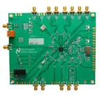


 工商网监
湘ICP备2023018690号
工商网监
湘ICP备2023018690号
