LMK04100, LMK04101, LMK04102, LMK04110
LMK04111, LMK04131, LMK04133
www.ti.com
SNAS516B – APRIL 2011 – REVISED NOVEMBER 2012
LMK04100 Family Clock Jitter Cleaner with Cascaded PLLs
Check for Samples: LMK04100, LMK04101, LMK04102, LMK04110, LMK04111, LMK04131, LMK04133
FEATURES
1
•
23
•
•
•
•
•
Cascaded PLLatinum™ PLL Architecture
– PLL1
– Redundant Reference Inputs
– Loss of Signal Detection
– Automatic and Manual Selection of
Reference Clock Input
– PLL2
– Phase Detector Rate up to 100 MHz
– Input Frequency-Doubler
– Integrated VCO
Outputs
– LVPECL/2VPECL, LVDS, and LVCMOS
Formats
– Support Clock Rates up to 1080 MHz
– Five Dedicated Channel Divider Blocks
– Common Output Frequencies Supported:
– 30.72 MHz, 61.44 MHz, 62.5 MHz, 74.25
MHz, 75 MHz, 77.76 MHz, 100 MHz,
106.25 MHz, 125 MHz, 122.88 MHz, 150
MHz, 155.52 MHz, 156.25 MHz, 159.375
MHz, 187.5 MHz, 200 MHz, 212.5 MHz,
245.76 MHz, 250 MHz, 311.04 MHz, 312.5
MHz, 368.64 MHz, 491.52 MHz, 622.08
MHz, 625 MHz, 983.04 MHz
MICROWIRE (SPI) Programming Interface
Industrial Temperature Range: -40 to 85 °C
3.15 V to 3.45 V Operation
Package: 48 Pin WQFN (7.0 x 7.0 x 0.8 mm)
APPLICATIONS
•
•
•
•
•
•
•
•
Multi-Carrier/Multi-Mode/Multi-Band 2G/3G/4G
Basestations
Cellular Repeaters
High Speed A/D clocking
SONET/SDH OC-48/OC-192/OC-768 Line Cards
GbE/10GbE, 1/2/4/8/10G Fibre Channel Line
Cards
Optical Transport Networks
Broadcast Video, HDTV
Serial ATA
DESCRIPTION
The LMK04100 family of precision clock conditioners
provides jitter cleaning, clock multiplication and
distribution without the need for high-performance
VCXO modules.
When connected to a recovered system reference
clock and a VCXO, the device generates 5 low jitter
clocks in LVCMOS, LVDS, or LVPECL formats.
External VCXO or
low cost crystal
OSCin (Single ended or differential)
Internal
VCO
CLKin0
CLKout4
PLL2
PLL1
CLKout3
CLKin1
CLKout2
CLK
DATA
CLKout1
PWire
Port
LE
CLKout0
GOE
SYNC*
1
2
3
Please be aware that an important notice concerning availability, standard warranty, and use in critical applications of
Texas Instruments semiconductor products and disclaimers thereto appears at the end of this data sheet.
PLLatinum is a trademark of Texas Instruments.
All other trademarks are the property of their respective owners.
PRODUCTION DATA information is current as of publication date.
Products conform to specifications per the terms of the Texas
Instruments standard warranty. Production processing does not
necessarily include testing of all parameters.
Copyright © 2011–2012, Texas Instruments Incorporated
�LMK04100, LMK04101, LMK04102, LMK04110
LMK04111, LMK04131, LMK04133
SNAS516B – APRIL 2011 – REVISED NOVEMBER 2012
www.ti.com
Table 1. Device Configuration Information
NSID
2VPECL / LVPECL
OUTPUTS
LMK04100SQ
LVDS OUTPUTS
LVCMOS OUTPUTS
VCO
3
4
1185 to 1296 MHz
LMK04101SQ
3
4
1430 to 1570 MHz
LMK04102SQ
3
4
1600 to 1750 MHz
LMK04110SQ
5
LMK04111SQ
5
LMK04131SQ
2
2
2
1430 to 1570 MHz
LMK04133SQ
2
2
2
1840 to 2160 MHz
1185 to 1296 MHz
1430 to 1570 MHz
Table 2. Device Output Format Information
NSID
CLKout0
CLKout1
CLKout2
CLKout3
CLKout4
LMK04100SQ
2VPECL / LVPECL
LVCMOS x 2
LVCMOS x 2
2VPECL / LVPECL
2VPECL / LVPECL
LMK04101SQ
2VPECL / LVPECL
LVCMOS x 2
LVCMOS x 2
2VPECL / LVPECL
2VPECL / LVPECL
LMK04102SQ
2VPECL / LVPECL
LVCMOS x 2
LVCMOS x 2
2VPECL / LVPECL
2VPECL / LVPECL
LMK04110SQ
2VPECL / LVPECL
2VPECL / LVPECL
2VPECL / LVPECL
2VPECL / LVPECL
2VPECL / LVPECL
LMK04111SQ
2VPECL / LVPECL
2VPECL / LVPECL
2VPECL / LVPECL
2VPECL / LVPECL
2VPECL / LVPECL
LMK04131SQ
LVDS
2VPECL / LVPECL
LVCMOS x 2
2VPECL / LVPECL
LVDS
LMK04133SQ
LVDS
2VPECL / LVPECL
LVCMOS x 2
2VPECL / LVPECL
LVDS
Table 3 shows a limited list of example frequencies. Multiple output frequencies can be programmed on a single
device provided that the VCO frequency and VCO divider values are the same.
2
Submit Documentation Feedback
Copyright © 2011–2012, Texas Instruments Incorporated
Product Folder Links: LMK04100 LMK04101 LMK04102 LMK04110 LMK04111 LMK04131 LMK04133
�LMK04100, LMK04101, LMK04102, LMK04110
LMK04111, LMK04131, LMK04133
www.ti.com
SNAS516B – APRIL 2011 – REVISED NOVEMBER 2012
Table 3. Example Configurations for Common Frequencies
(1)
OSCin (MHz)
VCO Divider
PLL2 N
25
2
30
VCO Frequency
(1)
Output Divider
Output
Frequency
Application
1500
12
62.5
GigE
25
2
30
1500
10
75
SATA
24.8832
2
25
1244.16
8
77.76
SONET
25
2
24
1200
6
100
PCI Express
26.5625
7
8
1487.5
2
106.25
Fibre Channel
25
2
30
1500
6
125
GigE
25
5
12
1500
2
150
SATA
24.8832
2
25
1244.16
4
155.52
SONET
25
2
25
1250
4
156.25
10 GigE
26.5625
2
25
1275
4
159.375
10-G Fibre
Channel
25
2
25
1500
4
187.5
12 GigE
25
3
16
1200
2
200
PCI Express
26.5625
3
16
1275
2
212.5
4-G Fibre
Channel
25
3
20
1500
2
250
GigE
24.8832
2
25
1244.16
2
311.04
SONET
25
2
25
1250
2
312.5
XGMII
24.8832
2
25
1244.16
1
622.08
SONET
25
2
25
1200
1
625
10 GigE
Use VCO Frequency to select proper device option
Copyright © 2011–2012, Texas Instruments Incorporated
Submit Documentation Feedback
Product Folder Links: LMK04100 LMK04101 LMK04102 LMK04110 LMK04111 LMK04131 LMK04133
3
�LMK04100, LMK04101, LMK04102, LMK04110
LMK04111, LMK04131, LMK04133
SNAS516B – APRIL 2011 – REVISED NOVEMBER 2012
www.ti.com
CPout1
Functional Block Diagram
LOS
CLKin0
CLKin0*
Mux
CLKin1
CLKin1*
R1 Divider
Phase
Detector
PLL1
N1 Divider
CPout2
LOS0
LOS
LOS1
2X
Mux
OSCin
OSCin*
R2 Divider
N2 Divider
Partially
Integrated
Loop Filter
Internal VCO
Phase
Detector
PLL2
Fout
VCO
Divider
Distribution
Path
Mux
CLKout4
CLKout4*
Divider
GOE
Device
Control
SYNC*
LD
CLKout3B
Mux
CLKout3A
Divider
CLKout2B
CLK
DATA
PWire
Port
Mux
Control
Registers
CLKout2A
Divider
LE
CLKout1
Mux
CLKout1*
Divider
CLKout0
Mux
Clock Buffers
4
Submit Documentation Feedback
CLKout0*
Divider
Copyright © 2011–2012, Texas Instruments Incorporated
Product Folder Links: LMK04100 LMK04101 LMK04102 LMK04110 LMK04111 LMK04131 LMK04133
�LMK04100, LMK04101, LMK04102, LMK04110
LMK04111, LMK04131, LMK04133
www.ti.com
SNAS516B – APRIL 2011 – REVISED NOVEMBER 2012
CLKout4*
CLKout4
Vcc14
CLKout3*
CLKout3
Vcc13
CLKout2*
CLKout2
Vcc12
CLKout1*
CLKout1
Vcc11
Connection Diagram
48
47
46
45
44
43
42
41
40
39
38
37
GND
1
36
Bias
Fout
2
35
CLKin1_LOS
Vcc1
3
34
CLKin0_LOS
CLKuWire
4
33
Vcc10
DATAuWire
5
32
CPout2
LEuWire
6
31
Vcc9
NC
7
30
Vcc8
Vcc2
8
29
OSCin*
LDObyp1
9
28
OSCin
LDObyp2
10
27
SYNC*
GOE
11
26
CLKin1*
LD
12
25
CLKin1
18
19
20
21
22
23
24
Vcc5
CLKin0
CLKin0*
Vcc6
CPout1
Vcc7
17
Vcc4
16
GND
CLKout0
15
DLD_BYP
14
CLKout0*
13
Vcc3
DAP
Figure 1. 48-Pin WQFN Package
Top Down View
PIN DESCRIPTIONS
Pin Number
Name(s)
1
GND
2
Fout
I/O
Type
Description
GND
Ground (For Fout Buffer)
O
ANLG
VCO Frequency Output Port
PWR
Power Supply for VCO Output Buffer
3
VCC1
4
CLKuWire
I
CMOS
Microwire Clock Input
5
DATAuWire
I
CMOS
Microwire Data Input
6
LEuWire
I
CMOS
Microwire Latch Enable Input
7
NC
8
VCC2
PWR
Power Supply for VCO
No Connection
9
LDObyp1
ANLG
LDO Bypass, bypassed to ground with a 10 µF capacitor
10
LDObyp2
ANLG
LDO Bypass, bypassed to ground with a 0.1 µF
capacitor
11
GOE
I
CMOS
Global Output Enable
12
LD
O
CMOS
Lock Detect and PLL multiplexer Output
13
VCC3
14
CLKout0
PWR
O
Copyright © 2011–2012, Texas Instruments Incorporated
LVDS/LVPECL
Power Supply for CLKout0
Clock Channel 0 Output
Submit Documentation Feedback
Product Folder Links: LMK04100 LMK04101 LMK04102 LMK04110 LMK04111 LMK04131 LMK04133
5
�LMK04100, LMK04101, LMK04102, LMK04110
LMK04111, LMK04131, LMK04133
SNAS516B – APRIL 2011 – REVISED NOVEMBER 2012
www.ti.com
PIN DESCRIPTIONS (continued)
(1)
(2)
Pin Number
Name(s)
I/O
Type
15
CLKout0*
O
LVDS/LVPECL
16
DLD_BYP
ANLG
DLD Bypass, bypassed to ground with a 0.47 µF
capacitor
17
GND
GND
Ground (Digital)
18
VCC4
PWR
Power Supply for Digital
19
VCC5
PWR
Power Supply for CLKin buffers and PLL1 R-divider
20
CLKin0
I
ANLG
Reference Clock Input Port for PLL1 - AC or DC
Coupled (1)
21
CLKin0*
I
ANLG
Reference Clock Input Port for PLL1 (complimentary) AC or DC Coupled (1)
22
VCC6
PWR
Power Supply for PLL1 Phase Detector and Charge
Pump
23
CPout1
ANLG
Charge Pump1 Output
24
VCC7
PWR
Power Supply for PLL1 N-Divider
25
CLKin1
I
ANLG
Reference Clock Input Port for PLL1 - AC or DC
Coupled (1)
26
CLKin1*
I
ANLG
Reference Clock Input Port for PLL1 (complimentary) AC or DC Coupled (2)
27
SYNC*
I
CMOS
Global Clock Output Synchronization
28
OSCin
I
ANLG
Reference oscillator Input for PLL2 - AC Coupled
29
OSCin*
I
ANLG
Reference oscillator Input for PLL2 - AC Coupled
30
VCC8
PWR
Power Supply for OSCin Buffer and PLL2 R-Divider
31
VCC9
PWR
Power Supply for PLL2 Phase Detector and Charge
Pump
32
CPout2
O
ANLG
Charge Pump2 Output
PWR
Power Supply for VCO Divider and PLL2 N-Divider
O
Description
Clock Channel 0* Output
33
VCC10
34
CLKin0_LOS
O
LVCMOS
Status of CLKin0 reference clock input
35
CLKin1_LOS
O
LVCMOS
Status of CLKin1 reference clock input
36
Bias
I
ANLG
Bias Bypass. AC coupled with 1 µF capacitor to Vcc1
37
VCC11
PWR
Power Supply for CLKout1
38
CLKout1
O
LVPECL/LVCMOS
Clock Channel 1 Output
39
CLKout1*
O
LVPECL/LVCMOS
Clock Channel 1* Output
40
VCC12
41
CLKout2
O
LVPECL/LVCMOS
PWR
Clock Channel 2 Output
42
CLKout2*
O
LVPECL/LVCMOS
Clock Channel 2* Output
PWR
Power Supply for CLKout2
43
VCC13
44
CLKout3
O
LVPECL
Clock Channel 3 Output
45
CLKout3*
O
LVPECL
Clock Channel 3* Output
PWR
Power Supply for CLKout3
46
VCC14
47
CLKout4
O
LVDS/LVPECL
Power Supply for CLKout4
Clock Channel 4 Output
48
CLKout4*
O
LVDS/LVPECL
Clock Channel 4* Output
DAP
DAP
DIE ATTACH PAD, connect to GND
The reference clock inputs may be either AC or DC coupled.
The reference clock inputs may be either AC or DC coupled.
These devices have limited built-in ESD protection. The leads should be shorted together or the device placed in conductive foam
during storage or handling to prevent electrostatic damage to the MOS gates.
6
Submit Documentation Feedback
Copyright © 2011–2012, Texas Instruments Incorporated
Product Folder Links: LMK04100 LMK04101 LMK04102 LMK04110 LMK04111 LMK04131 LMK04133
�LMK04100, LMK04101, LMK04102, LMK04110
LMK04111, LMK04131, LMK04133
www.ti.com
SNAS516B – APRIL 2011 – REVISED NOVEMBER 2012
Absolute Maximum Ratings (1) (2) (3) (4)
Parameter
Symbol
Ratings
Units
VCC
-0.3 to 3.6
V
VIN
-0.3 to (VCC + 0.3)
V
TSTG
-65 to 150
°C
Lead Temperature (solder 4 sec)
TL
+260
°C
Junction Temperature
TJ
125
°C
Differential Input Current (CLKinX/X*,
OSCin/OSCin*)
IIN
±5
mA
Supply Voltage
(5)
Input Voltage
Storage Temperature Range
(1)
(2)
(3)
(4)
(5)
"Absolute Maximum Ratings" indicate limits beyond which damage to the device may occur. Operating Ratings indicate conditions for
which the device is intended to be functional, but do not guarantee specific performance limits. For guaranteed specifications and test
conditions, see the Electrical Characteristics. The guaranteed specifications apply only to the test conditions listed.
This device is a high performance RF integrated circuit with an ESD rating up to 8 KV Human Body Model, up to 300 V Machine Model
and up to 1,250 V Charged Device Model and is ESD sensitive. Handling and assembly of this device should only be done at ESD-free
workstations.
Stresses in excess of the absolute maximum ratings can cause permanent or latent damage to the device. These are absolute stress
ratings only. Functional operation of the device is only implied at these or any other conditions in excess of those given in the operation
sections of the data sheet. Exposure to absolute maximum ratings for extended periods can adversely affect device reliability.
If Military/Aerospace specified devices are required, please contact the Texas Instruments Sales Office/Distributors for availability and
specifications.
Never to exceed 3.6 V.
Package Thermal Resistance
Package
48-Lead WQFN
(1)
(1)
θJA
θJ-PAD (Thermal Pad)
27.4° C/W
5.8° C/W
Specification assumes 16 thermal vias connect the die attach pad to the embedded copper plane on the 4-layer JEDEC board. These
vias play a key role in improving the thermal performance of the WQFN. It is recommended that the maximum number of vias be used in
the board layout.
Recommended Operating Conditions
Parameter
Ambient
Temperature
Supply Voltage
Symbol
Condition
Min
Typical
Max
Unit
TA
VCC = 3.3 V
-40
25
85
°C
3.15
3.3
3.45
V
VCC
Electrical Characteristics
(3.15 V ≤ VCC ≤ 3.45 V, -40 °C ≤ TA ≤ 85 °C. Typical values represent most likely parametric norms at VCC = 3.3 V, TA = 25
°C, at the Recommended Operating Conditions at the time of product characterization and are not guaranteed.)
Symbol
Parameter
Conditions
Min
Typ
Max
Units
Current Consumption
ICC_PD
Power Down Supply Current
0.7
LMK04100, LMK04101,
LMK04102
(2)
ICC_CLKS
Supply Current with all clocks
enabled, Fout disabled. (1)
LMK04110, LMK04111
(2)
LMK04131, LMK04133
(2)
(1)
(2)
mA
380
435
378
435
335
385
mA
Load conditions for output clocks: LVPECL: 50 Ω to VCC-2 V. 2VPECL: 50 Ω to VCC-2.36 V. LVDS: 100 Ω differential. LVCMOS: 10 pF.
Additional test conditions for ICC limits: CLKoutX_DIV = 510, PLL1 and PLL2 locked. (See Table 34 for more information)
Copyright © 2011–2012, Texas Instruments Incorporated
Submit Documentation Feedback
Product Folder Links: LMK04100 LMK04101 LMK04102 LMK04110 LMK04111 LMK04131 LMK04133
7
�LMK04100, LMK04101, LMK04102, LMK04110
LMK04111, LMK04131, LMK04133
SNAS516B – APRIL 2011 – REVISED NOVEMBER 2012
www.ti.com
Electrical Characteristics (continued)
(3.15 V ≤ VCC ≤ 3.45 V, -40 °C ≤ TA ≤ 85 °C. Typical values represent most likely parametric norms at VCC = 3.3 V, TA = 25
°C, at the Recommended Operating Conditions at the time of product characterization and are not guaranteed.)
Symbol
Parameter
Conditions
Min
Typ
Max
Units
CLKin0/0* and CLKin1/1* Input Clock Specifications
Clock Input Frequency
fCLKin
(3)
SLEWCLKin
Slew Rate on CLKin
(4)
VIDCLKin
VSSCLKin
Clock Input
Differential Input Voltage
(5)
VIDCLKin
Input Voltage Swing,
single-ended
VCLKin-offset
0.001
400
Auto-Switching mode
1
400
DC offset voltage between
CLKinX/CLKinX*
|CLKinX-CLKinX*|
0.5
MHz
20% to 80%
0.15
Each pin AC coupled
CLKinX_TYPE=0 (Bipolar)
0.25
1.55
|V|
CLKinX and CLKinX* are both
driven, AC coupled.
CLKinX_TYPE=0 (Bipolar)
0.5
3.1
Vpp
0.25
1.55
|V|
0.5
3.1
Vpp
AC coupled to CLKinX; CLKinX*
AC coupled to Ground
CLKinX_TYPE=0 (Bipolar)
0.25
2.0
Vpp
AC coupled to CLKinX; CLKinX*
AC coupled to Ground
CLKinX_TYPE=1 (MOS)
0.25
2.0
Vpp
CLKinX and CLKinX* are both
driven, AC coupled.
CLKinX_TYPE=1 (MOS)
VSSCLKin
VCLKin
Manual Select mode
V/ns
Each pin AC coupled
CLKinX_TYPE=0 (Bipolar)
44
mV
Each pin AC coupled
CLKinX_TYPE=1 (MOS)
294
mV
VCLKin-VIH
High Input Voltage
DC coupled to CLKinX; CLKinX*
AC coupled to Ground
CLKinX_TYPE=1 (MOS)
2.0
VCC
V
VCLKin-VIL
Low Input Voltage
DC coupled to CLKinX; CLKinX*
AC coupled to Ground
CLKinX_TYPE=1 (MOS)
0.0
0.4
V
(3)
(4)
(5)
8
CLKin0 and CLKin1 maximum of 400 MHz is guaranteed by characterization, production tested at 200 MHz.
In order to meet the jitter performance listed in the subsequent sections of this data sheet, the minimum recommended slew rate for all
input clocks is 0.5 V/ns. This is especially true for single-ended clocks. Phase noise performance will begin to degrade as the clock input
slew rate is reduced. However, the device will function at slew rates down to the minimum listed. When compared to single-ended
clocks, differential clocks (LVDS, LVPECL) will be less susceptible to degradation in phase noise performance at lower slew rates due to
their common mode noise rejection. However, it is also recommended to use the highest possible slew rate for differential clocks to
achieve optimal phase noise performance at the device outputs.
See Differential Voltage Measurement Terminology for definition of VID and VOD voltages.
Submit Documentation Feedback
Copyright © 2011–2012, Texas Instruments Incorporated
Product Folder Links: LMK04100 LMK04101 LMK04102 LMK04110 LMK04111 LMK04131 LMK04133
�LMK04100, LMK04101, LMK04102, LMK04110
LMK04111, LMK04131, LMK04133
www.ti.com
SNAS516B – APRIL 2011 – REVISED NOVEMBER 2012
Electrical Characteristics (continued)
(3.15 V ≤ VCC ≤ 3.45 V, -40 °C ≤ TA ≤ 85 °C. Typical values represent most likely parametric norms at VCC = 3.3 V, TA = 25
°C, at the Recommended Operating Conditions at the time of product characterization and are not guaranteed.)
Symbol
Parameter
Conditions
Min
Typ
Max
Units
40
MHz
PLL1 Specifications
fPD
PLL1 Phase Detector Frequency
ICPout1 SOURCE
ICPout1 SINK
PLL1 Charge Pump Source
Current (6)
PLL1 Charge Pump Sink Current
(6)
VCPout1 = VCC/2, PLL1_CP_GAIN
= 100b
25
VCPout1 = VCC/2, PLL1_CP_GAIN
= 101b
50
VCPout1 = VCC/2, PLL1_CP_GAIN
= 110b
100
VCPout1 = VCC/2, PLL1_CP_GAIN
= 111b
400
PLL1_CP_GAIN = 000b
NA
PLL1_CP_GAIN = 001b
NA
VCPout1=VCC/2, PLL1_CP_GAIN =
010b
20
VCPout1=VCC/2, PLL1_CP_GAIN =
011b
80
VCPout1=VCC/2, PLL1_CP_GAIN =
100b
-25
VCPout1=VCC/2, PLL1_CP_GAIN =
101b
-50
VCPout1=VCC/2, PLL1_CP_GAIN =
110b
-100
VCPout1=VCC/2, PLL1_CP_GAIN =
111b
-400
PLL1_CP_GAIN = 000b
NA
PLL1_CP_GAIN = 001b
NA
VCPout1=VCC/2, PLL1_CP_GAIN =
010b
-20
VCPout1=VCC/2, PLL1_CP_GAIN =
011b
-80
µA
µA
ICPout1 %MIS
Charge Pump Sink / Source
Mismatch
VCPout1 = VCC/2, T = 25 °C
3
ICPout1VTUNE
Magnitude of Charge Pump
Current vs. Charge Pump Voltage
Variation
0.5 V < VCPout1 < VCC - 0.5 V
TA = 25 °C
4
%
ICPout1 %TEMP
Charge Pump Current vs.
Temperature Variation
4
%
PLL1 ICPout1 TRI
Charge Pump TRI-STATE
Leakage Current
0.5 V < VCPout < VCC - 0.5 V
10
5
%
nA
PLL2 Reference Input (OSCin) Specifications
fOSCin
PLL2 Reference Input
EN_PLL2_REF 2X = 0
250
(8)
(7)
EN_PLL2_REF 2X = 1
SLEWOSCin
PLL2 Reference Clock minimum
slew rate on OSCin
VIDOSCin
Differential voltage swing
VSSOSCin
VOSCin
(6)
(7)
(8)
(9)
20% to 80%
(9)
AC coupled
Single-ended Input Voltage for
OSCin or OSCin*
AC coupled; Unused pin AC
coupled to GND
MHz
50
0.15
0.5
V/ns
0.2
1.55
|V|
0.4
3.1
Vpp
0.2
2.0
Vpp
This parameter is programmable
FOSCin maximum frequency guaranteed by characterization. Production tested at 200 MHz.
The EN_PLL2_REF2X bit (Register 13) enables/disables a frequency doubler mode for the PLL2 OSCin path.
See Differential Voltage Measurement Terminology for definition of VID and VOD voltages.
Copyright © 2011–2012, Texas Instruments Incorporated
Submit Documentation Feedback
Product Folder Links: LMK04100 LMK04101 LMK04102 LMK04110 LMK04111 LMK04131 LMK04133
9
�LMK04100, LMK04101, LMK04102, LMK04110
LMK04111, LMK04131, LMK04133
SNAS516B – APRIL 2011 – REVISED NOVEMBER 2012
www.ti.com
Electrical Characteristics (continued)
(3.15 V ≤ VCC ≤ 3.45 V, -40 °C ≤ TA ≤ 85 °C. Typical values represent most likely parametric norms at VCC = 3.3 V, TA = 25
°C, at the Recommended Operating Conditions at the time of product characterization and are not guaranteed.)
Symbol
Parameter
Conditions
Min
Typ
Max
Units
Crystal Oscillator Mode Specifications
fXTAL
Crystal Frequency Range
ESR
Crystal Effective Series Resistance 6 MHz < FXTAL < 20 MHz
6
PXTAL
Crystal Power Dissipation
CIN
Input Capacitance of LMK041xx
OSCin port
(10)
Vectron VXB1 crystal, 12.288
MHz, RESR < 40 Ω
-40 to +85 °C
20
MHz
100
Ohms
200
µW
6
pF
PLL2 Phase Detector and Charge Pump Specifications
fPD
Phase Detector Frequency
ICPoutSOURCE
ICPoutSINK
PLL2 Charge Pump Source
Current (6)
PLL2 Charge Pump Sink Current
(6)
100
VCPout2=VCC/2, PLL2_CP_GAIN =
00b
100
VCPout2=VCC/2, PLL2_CP_GAIN =
01b
400
VCPout2=VCC/2, PLL2_CP_GAIN =
10b
1600
VCPout2=VCC/2, PLL2_CP_GAIN =
11b
3200
VCPout2=VCC/2, PLL2_CP_GAIN =
00b
-100
VCPout2=VCC/2, PLL2_CP_GAIN =
01b
-400
VCPout2=VCC/2, PLL2_CP_GAIN =
10b
-1600
VCPout2=VCC/2, PLL2_CP_GAIN =
11b
-3200
MHz
µA
µA
ICPout2%MIS
Charge Pump Sink/Source
Mismatch
VCPout2=VCC/2, TA = 25 °C
3
ICPout2VTUNE
Magnitude of Charge Pump
Current vs. Charge Pump Voltage
Variation
0.5 V < VCPout2 < VCC - 0.5 V
TA = 25 °C
4
%
ICPout2%TEMP
Charge Pump Current vs.
Temperature Variation
4
%
ICPout2TRI
Charge Pump Leakage
0.5 V < VCPout2 < VCC - 0.5 V
10
10
%
nA
Internal VCO Specifications
fVCO
PVCO
VCO Tuning Range
VCO Output power to a
50 Ω load driven by Fout
LMK041x0
1185
1296
LMK041x1
1430
1570
LMK041x2
1600
1750
LMK041x3
1840
2160
LMK041x0, TA = 25 °C, singleended
3
LMK041x1, TA = 25 °C, singleended
3
LMK041x2, TA = 25 °C, singleended
2
LMK041x3, TA = 25 °C, singleended 1840 MHz
0
LMK041x3, TA = 25 °C, singleended 2160 MHz
-5
MHz
dBm
(10) See Application Section discussion of Crystal Power Dissipation.
10
Submit Documentation Feedback
Copyright © 2011–2012, Texas Instruments Incorporated
Product Folder Links: LMK04100 LMK04101 LMK04102 LMK04110 LMK04111 LMK04131 LMK04133
�LMK04100, LMK04101, LMK04102, LMK04110
LMK04111, LMK04131, LMK04133
www.ti.com
SNAS516B – APRIL 2011 – REVISED NOVEMBER 2012
Electrical Characteristics (continued)
(3.15 V ≤ VCC ≤ 3.45 V, -40 °C ≤ TA ≤ 85 °C. Typical values represent most likely parametric norms at VCC = 3.3 V, TA = 25
°C, at the Recommended Operating Conditions at the time of product characterization and are not guaranteed.)
Symbol
KVCO
|ΔTCL|
Parameter
Conditions
Fine Tuning Sensitivity
(The range displayed in the typical
column indicates the lower
sensitivity is typical at the lower
end of the tuning range, and the
higher tuning sensitivity is typical
at the higher end of the tuning
range).
Min
Typ
LMK041x0
7 to 9
LMK041x1
8 to 11
LMK041x2
9 to 14
LMK041x3
14 to 26
After programming R15 for lock,
no changes to output configuration
are permitted to guarantee
continuous lock
Allowable Temperature Drift for
Continuous Lock
(11)
Max
Units
MHz/V
125
°C
CLKout's Internal VCO Closed Loop Jitter Specifications using a Commercial Quality VCXO
JCLKout
12 kHz–20MHz
LMK041x0/
LMK041x1/
LMK041x2/
fCLKout = 122.88 MHz
Integrated RMS Jitter
LMK041x3
fCLKout = 122.88 MHz
Integrated RMS Jitter
JCLKout
1.875–20MHz
LMK041x0/
LMK041x1/
LMK041x3/
fCLKout = 153.6 MHz
Integrated RMS Jitter
LVDS
160
LVPECL 1600 mVpp
150
LVCMOS
140
LVDS
170
LVPECL 1600 mVpp
160
LVCMOS
150
LVDS
90
LVPECL 1600 mVpp
80
LVCMOS
75
fs
fs
fs
Digital Inputs (CLKuWire, DATAuWire, LEuWire)
VIH
High-Level Input Voltage
1.6
VIL
Low-Level Input Voltage
IIH
High-Level Input Current
VIH = VCC
IIL
Low-Level Input Current
VIL = 0
VIH
High-Level Input Voltage
VIL
Low-Level Input Voltage
IIH
High-Level Input Current
VIH = VCC
IIL
Low-Level Input Current
VIL = 0
VCC
V
0.4
V
-5
25
µA
-5.0
5.0
µA
1.6
VCC
V
0.4
V
-5.0
5.0
µA
-40.0
5.0
µA
Digital Inputs (GOE, SYNC*)
Digital Outputs (CLKinX_LOS, LD)
VOH
High-Level Output Voltage
IOH = -500 µA
VOL
Low-Level Output Voltage
IOL = 500 µA
VCC - 0.4
V
0.4
V
Default Power On Reset Clock Output Frequency
fCLKout-startup
Default output clock frequency at
device power on
CLKout2, LM041x0
50
CLKout2, LM041x1
62
CLKout2, LM041x2
68
CLKout2, LM041x3
81
MHz
(11) Maximum Allowable Temperature Drift for Continuous Lock is how far the temperature can drift in either direction from the value it was
at the time that the R0 register was last programmed, and still have the part stay in lock. The action of programming the R0 register,
even to the same value, activates a frequency calibration routine. This implies the part will work over the entire frequency range, but if
the temperature drifts more than the maximum allowable drift for continuous lock, then it will be necessary to reload the R0 register to
ensure it stays in lock. Regardless of what temperature the part was initially programmed at, the temperature can never drift outside the
frequency range of -40 °C to 85 °C without violating specifications.
Copyright © 2011–2012, Texas Instruments Incorporated
Submit Documentation Feedback
Product Folder Links: LMK04100 LMK04101 LMK04102 LMK04110 LMK04111 LMK04131 LMK04133
11
�LMK04100, LMK04101, LMK04102, LMK04110
LMK04111, LMK04131, LMK04133
SNAS516B – APRIL 2011 – REVISED NOVEMBER 2012
www.ti.com
Electrical Characteristics (continued)
(3.15 V ≤ VCC ≤ 3.45 V, -40 °C ≤ TA ≤ 85 °C. Typical values represent most likely parametric norms at VCC = 3.3 V, TA = 25
°C, at the Recommended Operating Conditions at the time of product characterization and are not guaranteed.)
Symbol
Parameter
Conditions
Min
Typ
Max
Units
LVDS Clock Outputs (CLKoutX)
fCLKout
TSKEW
VOD
VSS
Maximum Frequency
RL = 100 Ω
CLKoutX to CLKoutY
LVDS-LVDS, T = 25 °C,
FCLK = 800 MHz, RL= 100 Ω
(12)
1080
Differential Output Voltage
(13)
R = 100 Ω differential termination,
AC coupled to receiver input,
FCLK = 800 MHz,
T = 25 °C
MHz
30
ps
250
350
450
|mV|
500
700
900
mVpp
50
mV
1.375
V
35
|mV|
ΔVOD
Change in Magnitude of VOD for
complementary output states
VOS
Output Offset Voltage
ΔVOS
Change in VOS for complementary
output states
ISA
ISB
Output short circuit current - single Single-ended output shorted to
ended
GND, T = 25 °C
-24
24
mA
ISAB
Output short circuit current differential
-12
12
mA
TSKEW
CLKoutX to CLKoutY
(12)
Output High Voltage
VOL
Output Low Voltage
VOD
Output Voltage
(13)
1.25
(14)
Maximum Frequency
VOH
VSS
1.125
Complimentary outputs tied
together
LVPECL Clock Outputs (CLKoutX)
fCLKout
-50
1080
MHz
LVPECL-to-LVPECL,
T = 25 °C, FCLK = 800 MHz,
each output terminated with 120 Ω
to GND.
FCLK = 100 MHz, T = 25 °C
Termination = 50 Ω to
VCC - 2 V
40
ps
VCC 0.93
V
VCC 1.82
V
660
890
965
|mV|
1320
1780
1930
mVpp
(12) Equal loading and identical channel configuration on each channel is required for specification to be valid.
(13) See Differential Voltage Measurement Terminology for definition of VID and VOD voltages.
(14) LVPECL/2VPECL is programmable for all NSIDs.
12
Submit Documentation Feedback
Copyright © 2011–2012, Texas Instruments Incorporated
Product Folder Links: LMK04100 LMK04101 LMK04102 LMK04110 LMK04111 LMK04131 LMK04133
�LMK04100, LMK04101, LMK04102, LMK04110
LMK04111, LMK04131, LMK04133
www.ti.com
SNAS516B – APRIL 2011 – REVISED NOVEMBER 2012
Electrical Characteristics (continued)
(3.15 V ≤ VCC ≤ 3.45 V, -40 °C ≤ TA ≤ 85 °C. Typical values represent most likely parametric norms at VCC = 3.3 V, TA = 25
°C, at the Recommended Operating Conditions at the time of product characterization and are not guaranteed.)
Symbol
Parameter
Conditions
Min
Typ
Max
Units
2VPECL Clock Outputs (CLKoutX)
fCLKout
TSKEW
Maximum Frequency
CLKoutX to CLKoutY
(15)
VOH
Output High Voltage
VOL
Output Low Voltage
VOD
Output Voltage
VSS
1080
MHz
2VPECL-2VPECL, T=25 °C, FCLK
= 800 MHz, each output
terminated with 120 Ω to GND.
FCLK = 100 MHz, T = 25 °C
Termination = 50 Ω to
VCC - 2 V
(16)
40
ps
VCC 0.95
V
VCC 1.98
V
800
1030
1200
|mV|
1600
2060
2400
mVpp
LVCMOS Clock Outputs (CLKoutX)
fCLKout
Maximum Frequency
5 pF Load
250
VOH
Output High Voltage
1 mA Load
VCC - 0.1
MHz
VOL
Output Low Voltage
1 mA Load
IOH
Output High Current (Source)
VCC = 3.3 V, VO = 1.65 V
28
mA
IOL
Output Low Current (Sink)
VCC = 3.3 V, VO = 1.65 V
28
mA
TSKEW
Skew between any two LVCMOS
outputs, same channel or different
channel
RL = 50 Ω, CL = 10 pF,
T = 25 °C, FCLK = 100 MHz.
DUTYCLK
Output Duty Cycle
VCC/2 to VCC/2, FCLK = 100 MHz,
T = 25 °C (17)
TR
Output Rise Time
20% to 80%, RL = 50 Ω,
CL = 5 pF
400
ps
TF
Output Fall Time
80% to 20%, RL = 50 Ω,
CL = 5 pF
400
ps
LVPECL to LVDS skew
Same device, T = 25 °C,
250 MHz
-230
ps
LVDS to LVCMOS skew
Same device, T = 25 °C,
250 MHz
770
ps
LVCMOS to LVPECL skew
Same device, T = 25 °C,
250 MHz
-540
ps
V
0.1
(15)
45
50
V
100
ps
55
%
Mixed Clock Skew
TSKEW ChanX ChanY
Microwire Interface Timing
TCS
Data to Clock Setup Time
See MICROWIRE Input Timing
25
ns
TCH
Data to Clock Hold Time
See MICROWIRE Input Timing
8
ns
TCWH
Clock Pulse Width High
See MICROWIRE Input Timing
25
ns
TCWL
Clock Pulse Width Low
See MICROWIRE Input Timing
25
ns
TES
Clock to Latch Enable
Setup Time
See MICROWIRE Input Timing
25
ns
TCES
Enable to Clock Setup
See MICROWIRE Input Timing
25
ns
TEW
Load Enable Pulse Width
See MICROWIRE Input Timing
25
ns
(15) Equal loading and identical channel configuration on each channel is required for specification to be valid.
(16) See Differential Voltage Measurement Terminology for definition of VID and VOD voltages.
(17) Guaranteed by characterization.
Copyright © 2011–2012, Texas Instruments Incorporated
Submit Documentation Feedback
Product Folder Links: LMK04100 LMK04101 LMK04102 LMK04110 LMK04111 LMK04131 LMK04133
13
�LMK04100, LMK04101, LMK04102, LMK04110
LMK04111, LMK04131, LMK04133
SNAS516B – APRIL 2011 – REVISED NOVEMBER 2012
www.ti.com
Serial Data Timing Diagram
MSB
DATAuWire
D27
LSB
D26
D25
D24
D23
D0
A3
A2
A1
A0
CLKuWire
tCES
tCS
tCH
tCWH
tES
tCWL
LEuWire
tEWH
Register programming information on the DATAuWire pin is clocked into a shift register on each rising edge of
the CLKuWire signal. On the rising edge of the LEuWire signal, the register is sent from the shift register to the
register addressed. A slew rate of at least 30 V/µs is recommended for these signals. After programming is
complete the CLKuWire, DATAuWire, and LEuWire signals should be returned to a low state. If the CLKuWire or
DATAuWire lines are toggled while the VCO is in lock, as is sometimes the case when these lines are shared
with other parts, the phase noise may be degraded during this programming.
Figure 2. Charge Pump Current Specification Definitions
I1 = Charge Pump Sink Current at VCPout = VCC - ΔV
I2 = Charge Pump Sink Current at VCPout = VCC/2
I3 = Charge Pump Sink Current at VCPout = ΔV
I4 = Charge Pump Source Current at VCPout = VCC - ΔV
I5 = Charge Pump Source Current at VCPout = VCC/2
I6 = Charge Pump Source Current at VCPout = ΔV
ΔV = Voltage offset from the positive and negative supply rails. Defined to be 0.5 V for this device.
14
Submit Documentation Feedback
Copyright © 2011–2012, Texas Instruments Incorporated
Product Folder Links: LMK04100 LMK04101 LMK04102 LMK04110 LMK04111 LMK04131 LMK04133
�LMK04100, LMK04101, LMK04102, LMK04110
LMK04111, LMK04131, LMK04133
www.ti.com
SNAS516B – APRIL 2011 – REVISED NOVEMBER 2012
CHARGE PUMP OUTPUT CURRENT MAGNITUDE VARIATION VS. CHARGE PUMP OUTPUT
VOLTAGE
CHARGE PUMP SINK CURRENT VS. CHARGE PUMP OUTPUT SOURCE CURRENT MISMATCH
CHARGE PUMP OUTPUT CURRENT MAGNITUDE VARIATION VS. TEMPERATURE
Differential Voltage Measurement Terminology
The differential voltage of a differential signal can be described by two different definitions causing confusion
when reading datasheets or communicating with other engineers. This section will address the measurement and
description of a differential signal so that the reader will be able to understand and discern between the two
different definitions when used.
The first definition used to describe a differential signal is the absolute value of the voltage potential between the
inverting and non-inverting signal. The symbol for this first measurement is typically VID or VOD depending on if
an input or output voltage is being described.
The second definition used to describe a differential signal is to measure the potential of the non-inverting signal
with respect to the inverting signal. The symbol for this second measurement is VSS and is a calculated
parameter. Nowhere in the IC does this signal exist with respect to ground, it only exists in reference to its
differential pair. VSS can be measured directly by oscilloscopes with floating references, otherwise this value can
be calculated as twice the value of VOD as described in the first description.
Figure 11 illustrates the two different definitions side-by-side for inputs and Figure 12 illustrates the two different
definitions side-by-side for outputs. The VID and VOD definitions show VA and VB DC levels that the non-inverting
and inverting signals toggle between with respect to ground. VSS input and output definitions show that if the
inverting signal is considered the voltage potential reference, the non-inverting signal voltage potential is now
increasing and decreasing above and below the non-inverting reference. Thus the peak-to-peak voltage of the
differential signal can be measured.
VID and VOD are often defined as volts (V) and VSS is often defined as volts peak-to-peak (VPP).
VID Definition
VSS Definition for Input
Non-Inverting Clock
VA
2· VID
VID
VB
Inverting Clock
VID = | VA - VB |
VSS = 2· VID
GND
Figure 3. Two Different Definitions for Differential Input Signals
Copyright © 2011–2012, Texas Instruments Incorporated
Submit Documentation Feedback
Product Folder Links: LMK04100 LMK04101 LMK04102 LMK04110 LMK04111 LMK04131 LMK04133
15
�LMK04100, LMK04101, LMK04102, LMK04110
LMK04111, LMK04131, LMK04133
SNAS516B – APRIL 2011 – REVISED NOVEMBER 2012
www.ti.com
VOD Definition
VSS Definition for Output
Non-Inverting Clock
VA
2· VOD
VOD
VB
Inverting Clock
VOD = | VA - VB |
VSS = 2· VOD
GND
Refer to application note AN-912 Common Data Transmission Parameters and their Definitions (SNLA036) for more
information.
Figure 4. Two Different Definitions for Differential Output Signals
16
Submit Documentation Feedback
Copyright © 2011–2012, Texas Instruments Incorporated
Product Folder Links: LMK04100 LMK04101 LMK04102 LMK04110 LMK04111 LMK04131 LMK04133
�LMK04100, LMK04101, LMK04102, LMK04110
LMK04111, LMK04131, LMK04133
www.ti.com
SNAS516B – APRIL 2011 – REVISED NOVEMBER 2012
Typical Performance Characteristics
CLOCK OUTPUT AC CHARACTERISTICS
LVPECL VOD
vs.
Frequency
DIFFERENTIAL P-P VOLTAGE (mV)
DIFFERENTIAL P-P VOLTAGE (mV)
LVDS VOD
vs.
Frequency
1.0
0.9
0.8
0.7
0.6
0.5
0.4
0.3
0.2
0.1
0.0
0
300
600
900
1.2k
1.5k
2.5
2.0
LV2PECL Mode
1.5
1.0
NORMAL Mode
0.5
0.0
0
1.8k
400
5
1.2k
1.6k
2k
Figure 5.
Figure 6.
LVCMOS Vpp
vs.
Frequency
Typical Dynamic ICC, LVCMOS Driver, VCC = 3.3 V,
Temp = 25 °C, CL= 5 pF
No Load
10 pF Load
22 pF Load
4
3
2
47 pF Load
1
800
FREQUENCY (MHz)
ICC (mA)
SINGLE-ENDED P-P VOLTAGE (V)
FREQUENCY (MHz)
40
35
30
25
20
15
10
5
0
100 pF Load
0
0
100
200
300
400
500
0
FREQUENCY (MHz)
50
100 150 200 250 300 350 400
FREQUENCY (MHz)
Figure 7.
Figure 8.
NOISE FLOOR (dBc/Hz)
Clock Output Noise Floor
vs.
Frequency
-130
-135
-140
LVPECL (differential)
-145
-150 LVDS (differential)
-155
-160
-165
-170
LVCMOS
10
100
1000
FREQUENCY (MHz)
To estimate this noise, only the output frequency is required. Divide value and input frequency are not relevant.
Figure 9.
Copyright © 2011–2012, Texas Instruments Incorporated
Submit Documentation Feedback
Product Folder Links: LMK04100 LMK04101 LMK04102 LMK04110 LMK04111 LMK04131 LMK04133
17
�LMK04100, LMK04101, LMK04102, LMK04110
LMK04111, LMK04131, LMK04133
SNAS516B – APRIL 2011 – REVISED NOVEMBER 2012
www.ti.com
FEATURES
SYSTEM ARCHITECTURE
The cascaded PLL architecture of the LMK041xx was chosen to provide the lowest jitter performance over the
widest range of output frequencies and phase noise offset frequencies. The first stage PLL (PLL1) is used in
conjunction with an external reference clock and an external VCXO to provide a frequency accurate, low phase
noise reference clock for the second stage frequency multiplication PLL (PLL2). PLL1 typically uses a narrow
loop bandwidth (10 Hz to 200 Hz) to retain the frequency accuracy of the reference clock input signal while at the
same time suppressing the higher offset frequency phase noise that the reference clock may have accumulated
along its path or from other circuits. The “cleaned” reference clock frequency accuracy is combined with the low
phase noise of an external VCXO to provide the reference input to PLL2. The low phase noise reference
provided to PLL2 allows it to use wider loop bandwidths (50 kHz to 200 kHz). The chosen loop bandwidth for
PLL2 should take best advantage of the superior high offset frequency phase noise profile of the internal VCO
and the good low offset frequency phase noise of the reference VCXO for PLL2. Low jitter is achieved by
allowing the external VCXO’s phase noise to dominate the final output phase noise at low offset frequencies and
the internal VCO’s phase noise to dominate the final output phase noise at high offset frequencies. This results in
best overall phase noise and jitter performance.
REDUNDANT REFERENCE INPUTS (CLKin0/CLKin0*, CLKin1/CLKin1*)
The LMK041xx has two LVDS/LVPECL/LVCMOS compatible reference clock inputs for PLL1, CLKin0 and
CLKin1. The selection of the preferred input may be fixed to either CLKin0 or CLKin1, or may be configured to
employ one of two automatic switching modes when redundant clock signals are present. The PLL1 reference
clock input buffers may also be individually configured as either a CMOS buffered input or a bipolar buffered
input.
PLL1 CLKinX (X=0,1) LOSS OF SIGNAL (LOS)
When either of the two auto-switching modes is selected for the reference clock input mode, the signal status of
the selected reference clock input is indicated by the state of the CLKinX_LOS (loss-of-signal) output. These
outputs may be configured as either CMOS (active HIGH on loss-of-signal), NMOS open-drain or PMOS opendrain. If PLL1 was originally locked and then both reference clocks go away, then the frequency accuracy of the
LMK04100 device will be set by the absolute tuning range of the VCXO used on PLL1. The absolute tuning
range of the VCXO can be determined by multiplying its' tuning constant by the charge pump voltage.
INTEGRATED LOOP FILTER POLES
The LMK041xx features programmable 3rd and 4th order loop filter poles for PLL2. When enabled, internal
resistors and capacitor values may be selected from a fixed range of values to achieve either 3rd or 4th order
loop filter response. These programmable components compliment external components mounted near the chip.
CLOCK DISTRIBUTION
The LMK041xx features a clock distribution block with a minimum of five outputs that are a mixture of LVPECL,
2VPECL, LVDS, and LVCMOS. The exact combination is determined by the part number. The 2VPECL is a
Texas Instruments proprietary configuration that produces a 2 Vpp differential swing for compatibility with many
data converters. More than five outputs may be available for device versions that offer dual LVCMOS outputs.
CLKout DIVIDE (CLKoutX_DIV, X = 0 to 4)
Each individual clock distribution channel includes a channel divider. The range of divide values is 2 to 510, in
steps of 2. “Bypass” mode operates as a divide-by-1.
GLOBAL CLOCK OUTPUT SYNCHRONIZATION (SYNC*)
The SYNC* input is used to synchronize the active clock outputs. When SYNC* is held in a logic low state, the
outputs are also held in a logic low state. When SYNC* goes high, the clock outputs are activated and will
transition to a high state simultaneously with one another.
18
Submit Documentation Feedback
Copyright © 2011–2012, Texas Instruments Incorporated
Product Folder Links: LMK04100 LMK04101 LMK04102 LMK04110 LMK04111 LMK04131 LMK04133
�LMK04100, LMK04101, LMK04102, LMK04110
LMK04111, LMK04131, LMK04133
www.ti.com
SNAS516B – APRIL 2011 – REVISED NOVEMBER 2012
SYNC* must be held low for greater than one clock cycle of the Clock Distribution Path. After this low event has
been registered, the outputs will not reflect the low state for four more cycles. Similarly after SYNC* becomes
high, the outputs will simultaneously transition high after four Clock Distribution Path cycles have passed. See
Figure 10 for further detail.
Distribution
Path
SYNC*
CLKout0
CLKout1
CLKout2
Figure 10. Clock Output synchronization using the SYNC* pin
GLOBAL OUTPUT ENABLE AND LOCK DETECT
Each Clock Output Channel may be either enabled or put into a high impedance state via the Clock Output
Enable control bit (one for each channel). Each output enable control bit is gated with the Global Output Enable
input pin (GOE). The GOE pin provides an internal pull-up so that if it is un-terminated externally, then the clock
output states are determined by the Clock Channel Output Enable Register bits. All clock outputs can be
disabled simultaneously if the GOE pin is pulled low by an external signal.
Table 4. Clock Output Control
CLKoutX
_EN bit
EN_CLKout
_Global bit
GOE pin
CLKoutX Output State
1
1
Low
Low
Don't care
0
Don't care
Off
0
Don't care
Don't care
Off
1
1
High / No Connect
Enabled
The Lock Detect (LD) signal can be connected to the GOE pin in which case all outputs are disabled
automatically if the synthesizer is not locked. See EN_CLKoutX: Clock Channel Output Enable and also
SYSTEM LEVEL DIAGRAM for actual implementation details.
The Lock Detect (LD) pin can be programmed to output a ‘High’ when both PLL1 and PLL2 are locked, or only
when PLL1 is locked or only when PLL2 is locked.
Functional Description
ARCHITECTURAL OVERVIEW
The LMK041xx chip consists of two high performance synthesizer blocks (Phase Locked Loop, internal
VCO/VCO Divider, and loop filter), source selection, distribution system, and independent clock output channels.
The Phase Frequency Detector in PLL1 compares the divided (R Divider 1) system clock signal from the
selected CLKinX and CLKinX* input with the divided (N Divider 1) output of the external VCXO attached to the
PLL2 OSCin port. The external loop filter for PLL1 should be narrow to provide an clean reference clock from the
external VCXO to the OSCin/OSCin* pins for PLL2.
Copyright © 2011–2012, Texas Instruments Incorporated
Submit Documentation Feedback
Product Folder Links: LMK04100 LMK04101 LMK04102 LMK04110 LMK04111 LMK04131 LMK04133
19
�LMK04100, LMK04101, LMK04102, LMK04110
LMK04111, LMK04131, LMK04133
SNAS516B – APRIL 2011 – REVISED NOVEMBER 2012
www.ti.com
The Phase Frequency Detector in PLL2 then compares the divided (R Divider 2) reference signal from the PLL2
OSCin port with the divided (N Divider 2 and VCO Divider) output of the internal VCO. The bandwidth of the
external loop filter for PLL2 should be designed to be wide enough to take advantage of the low in-band phase
noise of PLL2 and the low high offset phase noise of the internal VCO. The VCO output is passed through a
common VCO divider block and placed on a distribution path for the clock distribution section. It is also routed to
the PLL2_N counter. Each clock output channel allows the user to select a path with a programmable divider
block, a phase synchronization circuit, and LVDS/LVPECL/2VPECL/LVCMOS compatible output buffers.
PHASE DETECTOR 1 (PD1)
Phase Detector 1 in PLL1 (PD1) can operate up to 40 MHz. Since a narrow loop bandwidth should be used for
PLL1, the need to operate at high phase detector rate to lower the in-band phase noise becomes unnecessary.
PHASE DETECTOR 2 (PD2)
Phase Detector 2 in PLL2 (PD2) supports a maximum comparison rate of 100 MHz, though the actual maximum
frequency at the input port (PLL2 OSCin/OSCin*) is 250 MHz. Operating at highest possible phase detector rate
will ensure low in-band phase noise for PLL2 which in turn produces lower total jitter, as the in-band phase noise
from the reference input and PLL are proportional to N2.
PLL2 FREQUENCY DOUBLER
The PLL2 reference input at the OSCin port may be optionally routed through a frequency doubler function rather
than through the PLL2_R counter. The maximum phase comparison frequency of the PLL2 phase detector is 100
MHz, so the input to the frequency doubler is limited to a maximum of 50 MHz. The frequency doubler feature
allows the phase comparison frequency to be increased when a relative low frequency oscillator is driving the
OSCin port. By doubling the PLL2 phase comparison frequency, the in-band PLL2 noise is reduced by about 3
dB.
INPUTS / OUTPUTS
PLL1 Reference Inputs (CLKin0 / CLKin0*, CLKin1 / CLKin1*)
The reference clock inputs for PLL1 may be selected from either CLKin0 and CLKin1. The user has the capability
to manually select one of the two inputs or to configure an automatic switching mode operation. A detailed
description of this function is described in the uWire programming section of this data sheet.
PLL2 OSCin / OSCin* Port
The feedback from the external oscillator being locked with PLL1 is injected to the PLL2 OSCin/OSCin* pins.
This input may be driven with either an AC coupled single-ended or AC coupled differential signal. If operated in
single ended mode, the unused input should be tied to GND with a 0.1 µF capacitor. Internal to the chip, this
signal is routed to the PLL1_N Counter and to the reference input for PLL2. The internal circuitry of the OSCin
port also supports the optional implementation of a crystal based oscillator circuit. A crystal, varactor diode and a
small number of other external components may be used to implement the oscillator. The internal oscillator
circuit is enabled by setting the EN_PLL2_XTAL bit.
CPout1 / CPout2
The CPout1 pin provides the charge pump current output to drive the loop filter for PLL1. This loop filter should
be configured so that the total loop bandwidth for PLL1 is less than 200 Hz. When combined with an external
oscillator that has low phase noise at offsets close to the carrier, PLL1 generates a reference for PLL2 that is
frequency locked to the PLL1 reference clock but has the phase noise performance of the oscillator. The CPout2
pin provides the charge pump current output to drive the loop filter for PLL2. This loop filter should be configured
so that the total loop bandwidth for PLL2 is in the range of 50 kHz to 200 kHz. See the section on uWire device
control for a description of the charge pump current gain control.
Fout
The buffered output of the internal VCO is available at the Fout pin. This is a single-ended output (sinusoid).
Each time the PLL2_N counter value is updated via the uWire interface, an internal algorithm is triggered that
optimizes the VCO performance.
20
Submit Documentation Feedback
Copyright © 2011–2012, Texas Instruments Incorporated
Product Folder Links: LMK04100 LMK04101 LMK04102 LMK04110 LMK04111 LMK04131 LMK04133
�LMK04100, LMK04101, LMK04102, LMK04110
LMK04111, LMK04131, LMK04133
www.ti.com
SNAS516B – APRIL 2011 – REVISED NOVEMBER 2012
Digital Lock Detect 1 Bypass
The VCO coarse tuning algorithm requires a stable OSCin clock (reference clock to PLL2) to frequency calibrate
the internal VCO correctly. In order to ensure a stable OSCin clock, the first PLL must achieve lock status. A
digital lock detect is used in PLL1 to monitor its lock status. After lock is achieved by PLL1, the coarse tuning
circuitry is enabled and frequency calibration for the internal VCO begins.
The (DLD_BYP) pin is provided to allow an external bypass cap to be connected to the digital lock detect 1. This
capacitor will eliminate potential glitches at initial startup of PLL1 due to unknown phase relationships between
the Ncntr1 and Rcntr1.
Bias
Proper bypassing of this pin by a 1 µF capacitor connected to VCC is important for low noise performance.
General Programming Information
LMK041xx devices are programmed using several 32-bit registers. Each register consists of a 4-bit address field
and 28-bit data field. The address field is formed by bits 0 through 3 (LSBs) and the data field is formed by bits 4
through 31 (MSBs). The contents of each register are clocked in MSB first (bit 31), and the LSB (bit 0) last.
During programming, the LE signal should be held LOW. The serial data is clocked in on the rising edge of the
CLK signal. After the LSB (bit 0) is clocked in the LE signal should be toggled LOW-to-HIGH-to-LOW to latch the
contents into the register selected in the address field. Registers R0-R4, R7, and R8-R15 must be programmed
in order to achieve proper device operation. Figure 11 illustrates the serial data timing sequence.
MSB
DATAuWire
D27
LSB
D26
D25
D24
D23
D0
A3
A2
A1
A0
CLKuWire
tCES
tCS
tCH
tCWH
tCWL
tES
LEuWire
tEWH
Figure 11. uWire Timing Diagram
To achieve proper frequency calibration, the OSCin port must be driven with a valid signal before programming
Register 15. Changes to PLL2_R Counter or the OSCin port signal require Register 15 to be reloaded in order to
activate the frequency calibration process.
RECOMMENDED PROGRAMMING SEQUENCE
The recommended programming sequence involves programming R7 with the reset bit set to 1 (Reg. 7, bit 4) to
ensure the device is in a default state. If R7 is programmed again, the reset bit should be set to 0. Registers are
programmed in order with R15 being the last register programmed. An example programming sequence is
shown below:
• Program R7 with the RESET bit = 1 (b4 = 1). This ensures that the device is configured with default settings.
When RESET = 1, all other R7 bits are ignored.
– If R7 is programmed again during the initial configuration of the device, the RESET bit should be cleared
(b4 = 0)
• Program R0 through R4 as necessary to configure the clock outputs as desired. These registers configure
clock channel functions such as the channel multiplexer output selection, divide value, and enable/disable bit.
• Program R5 and R6 with the default values shown in the register map on the following pages.
• Program R7 with RESET = 0.
• Program R8 through R10 with the default values shown in the register map on the following pages.
• Program R11 to configure the reference clock inputs (CLKin0 and CLKin1).
– type, LOS timeout, LOS type, and mode (manual or auto-switching)
• Program R12 to configure PLL1.
Copyright © 2011–2012, Texas Instruments Incorporated
Submit Documentation Feedback
Product Folder Links: LMK04100 LMK04101 LMK04102 LMK04110 LMK04111 LMK04131 LMK04133
21
�LMK04100, LMK04101, LMK04102, LMK04110
LMK04111, LMK04131, LMK04133
SNAS516B – APRIL 2011 – REVISED NOVEMBER 2012
•
www.ti.com
– Charge pump gain, polarity, R counter and N counter
Program R13 through R15 to configure PLL2 parameters, crystal mode options, and certain globally asserted
functions.
The following table provides the register map for device programming:
22
Submit Documentation Feedback
Copyright © 2011–2012, Texas Instruments Incorporated
Product Folder Links: LMK04100 LMK04101 LMK04102 LMK04110 LMK04111 LMK04131 LMK04133
�LMK04100, LMK04101, LMK04102, LMK04110
LMK04111, LMK04131, LMK04133
www.ti.com
SNAS516B – APRIL 2011 – REVISED NOVEMBER 2012
Table 5. Register Map
Register
31
30
29
28
27
26
25
24
23
22
21
20
19
18
17
16
15
14
13
12
11
10
9
8
7
6
5
4
1
CLKout0_PECL_LVL
R1
0
0
0
0
0
0
0
1
CLKout1_PECL_LVL
R2
0
0
0
0
0
0
0
1
CLKout2_PECL_LVL
R3
0
0
0
0
0
0
0
1
R4
0
0
0
0
0
0
0
1
R5
0
0
0
0
0
0
0
0
R6
0
0
0
0
1
0
0
0
0
0
0
0
CLKout0_
MUX
CLKout1_
MUX [1:0]
CLKout2_
MUX [1:0]
CLKout3_
MUX [1:0]
CLKout4_
MUX [1:0]
EN_CLKout0
0
CLKout0_DIV [7:0]
0
0
0
0
0
0
0
0
EN_CLKout1
0
0
A
0
CLKout1_DIV [7:0]
0
0
0
0
0
0
0
1
EN_CLKout2
0
1
A
1
CLKout2_DIV [7:0]
0
0
0
0
0
0
1
0
EN_CLKout3
0
2
A
2
CLKout3_DIV [7:0]
0
0
0
0
0
0
1
1
EN_CLKout4
0
CLKout3A_STATE [1:0] CLKout2A_STATE [1:0] CLKout1A_STATE [1:0]
0
CLKout3B_STATE [1:0] CLKout2B_STATE [1:0] CLKout1B_STATE [1:0]
0
3
A
3
CLKout4_DIV [7:0]
0
0
0
0
0
1
0
0
CLKout4_PECL_LVL
R0
CLKout3_PECL_LVL
Data [31:4]
0
0
0
0
0
0
0
0
0
0
0
0
0
0
0
0
0
0
0
0
0
0
0
0
0
1
0
1
0
0
0
0
0
0
0
0
0
0
0
0
0
0
0
0
0
1
1
1
0
1
1
0
Copyright © 2011–2012, Texas Instruments Incorporated
Product Folder Links: LMK04100 LMK04101 LMK04102 LMK04110 LMK04111 LMK04131 LMK04133
Submit Documentation Feedback
23
�LMK04100, LMK04101, LMK04102, LMK04110
LMK04111, LMK04131, LMK04133
SNAS516B – APRIL 2011 – REVISED NOVEMBER 2012
www.ti.com
28
27
26
25
24
23
22
21
20
19
18
17
16
15
14
13
12
11
10
9
8
7
6
5
4
3
2
1
0
R7
0
0
0
0
0
0
0
0
0
0
0
0
0
0
0
0
0
0
0
0
0
0
0
0
0
0
0
RESET
0
1
1
1
R8
0
0
0
0
0
0
0
0
0
0
0
0
0
0
0
0
0
0
0
0
0
0
0
0
0
0
0
0
1
0
0
0
R9
0
0
0
0
0
0
0
0
1
0
1
0
0
0
1
0
0
0
1
0
1
0
1
0
0
0
0
0
1
0
0
1
R10
0
0
RC_DLD1_Start
0
0
0
0
1
0
1
0
1
0
0
0
0
0
0
0
0
0
0
0
0
0
0
0
0
1
0
1
0
R11
0
0
0
0
0
0
0
0
0
1
1
0
0
1
0
1
0
0
0
0
CLKin1_BUFTYPE
CLKin0_BUFTYPE
1
0
1
1
R12
1
1
0
0
R13
0
0
0
1
1
0
1
R14
0
0
0
1
1
1
0
R15
0
0
0
1
1
1
1
24
PLL1_CP_
GAIN [2:0]
1
PLL2_CP_GAIN [1:0]
OSCin_FREQ [7:0]
Submit Documentation Feedback
VCO_DIV [3:0]
0
0
PLL_MUX [4:0]
PLL1 CP TRI-STATE
0
PLL2 CP TRI-STATE
0
EN_PLL2_REF2X
1
POWER DOWN, default = 0
0
PLL1_N Counter [11:0]
EN_CLKout_Global, default=1
1
EN_Fout
0
EN_PLL2_XTAL
PLL1_R Counter [11:0]
CLKin_SEL [1:0]
29
LOS_TYPE [1:0]
30
LOS_TIMEOUT [1:0]
31
PLL1_CP_POL
Table 5. Register Map (continued)
Register
PLL2_R4_LF [2:0] PLL2_R3_LF [2:0]
PLL2_R Counter [11:0]
PLL2_N Counter [17:0]
PLL2_C3_C4_LF [3:0]
Copyright © 2011–2012, Texas Instruments Incorporated
Product Folder Links: LMK04100 LMK04101 LMK04102 LMK04110 LMK04111 LMK04131 LMK04133
�LMK04100, LMK04101, LMK04102, LMK04110
LMK04111, LMK04131, LMK04133
www.ti.com
SNAS516B – APRIL 2011 – REVISED NOVEMBER 2012
DEFAULT DEVICE REGISTER SETTINGS AFTER POWER ON/RESET
Table 6 illustrates the default register settings programmed in silicon for the LMK041xx after power on or
asserting the reset bit.
Table 6. Default Device Register Settings after Power On/Reset
Field Name
Default
Value
(decimal)
Default State
Field Description
Register
Bit Location
(MSB:LSB)
CLKoutX_PECL_LVL
0
2VPECL disabled
This bit sets LVPECL clock level. Valid when
the clock channel is configured as
LVPECL/2VPECL; otherwise, not relevant.
R0 to R4
23
CLKoutXB_STATE
0
Inverted
This field sets the state of output B of an
LVCMOS Clock channel.
R1 to R3
22:21
CLKoutXA_STATE
1
Non-Inverted
This field sets the state of output A of an
LVCMOS Clock channel.
R1 to R3
20:19
EN_CLKoutX
0
OFF
Clock Channel enable bit. Note: The state of
CLKout2 is ON by default.
R0 to R4
16
R5,R6,R8
R9,R10
NA
Forces the VCO tuning algorithm state
machine to wait until PLL1 is locked.
R10
29
(1)
Reserved Registers
(1)
RC_DLD1_Start
1
Enabled
CLKin1_BUFTYPE
1
MOS mode
CLKin1 Input Buffer Type
R11
11
CLKin0_BUFTYPE
1
MOS mode
CLKin0 Input Buffer Type
R11
10
LOS_TIMEOUT
1
3 MHz (min.)
Selects Lower Reference Clock input
frequency for LOS Detection.
R11
9:8
LOS_TYPE
3
CMOS
Selects LOS output type
R11
7:6
CLKin_SEL
0
CLKin0
Selects Reference Clock source
R11
5:4
PLL1 CP Polarity
1
Positive polarity
Selects the charge pump output polarity, i.e.,
the tuning slope of the external VCXO
R12
31
PLL1_CP_GAIN
6
100 µA
Sets the PLL1 Charge Pump Gain
R12
30:28
PLL1_R Counter
1
Divide = 1
Sets divide value for PLL1_R Counter
R12
27:16
PLL1_N Counter
1
Divide = 1
Sets divide value for PLL1_N Counter
R12
15:4
EN_PLL2_REF2X
0
Disabled
Enables or disables the OSCin frequency
doubler path for the PLL2 reference input
R13
16
EN_PLL2_XTAL
0
OFF
Enables or Disables internal circuits that
support an external crystal driving the OSCin
pins
R13
21
EN_Fout
0
OFF
Enables or disables the VCO output buffer
R13
20
CLK Global Enable
1
Enabled
Global enable or disable for output clocks
R13
18
POWER DOWN
0
R13
17
PLL2 CP TRI-STATE
0
TRI-STATE
disabled
Enables or disables TRI-STATE for PLL2
Charge Pump
R13
15
PLL1 CP TRI-STATE
0
TRI-STATE
disabled
Enables or disables TRI-STATE for PLL1
Charge Pump
R13
14
(2)
Disabled (device is Device power down control
active)
OSCin_FREQ
200
200 MHz
Source frequency driving OSCin port
R14
28:21
PLL_MUX
31
Reserved
Selects output routed to LD pin
R14
20:16
PLL2_R Counter
1
Divide = 1
Sets Divide value for PLL2_R Counter
R14
15:4
PLL2_CP_GAIN
2
1600 µA
Sets PLL2 Charge Pump Gain
R15
27:26
VCO_DIV
2
Divide = 2
Sets divide value for VCO output divider
R15
25:22
PLL2_N Counter
1
Divide = 1
Sets PLL2_N Counter value
R15
21:4
(1)
(2)
These registers are reserved. The Power On/Reset values for these registers are shown in the register map and should not be changed
during programming.
If the CLKin_SEL value is set to either [0,0] or [0,1], the LOS_TYPE field should be set to [0,0].
Copyright © 2011–2012, Texas Instruments Incorporated
Submit Documentation Feedback
Product Folder Links: LMK04100 LMK04101 LMK04102 LMK04110 LMK04111 LMK04131 LMK04133
25
�LMK04100, LMK04101, LMK04102, LMK04110
LMK04111, LMK04131, LMK04133
SNAS516B – APRIL 2011 – REVISED NOVEMBER 2012
www.ti.com
REGISTER R0 TO R4
Registers R0 through R4 control the five clock outputs. Register R0 controls CLKout0, Register R1 controls
CLKout1, and so on. Aside from this, the functions of the bits in these registers are identical. The X in
CLKoutX_MUX, CLKoutX_DIV, and CLKoutX_EN denote the actual clock output which may be from 0 to 4.
CLKoutX_DIV: Clock Channel Divide Registers
Each of the five clock output channels (0 though 4) has a dedicated 8-bit divider followed by a fixed divide by 2
that is used to generate even integer related versions of the distribution path clock frequency (VCO Divider
output). If the VCO Divider value is even then the Channel Divider may be bypassed (See CLK Output Mux),
giving an effective divisor of 1 while preserving a 50% duty cycle output waveform.
Table 7. CLKoutX_DIV: Clock Channel Divide Values
CLKoutX_DIV [ 7:0 ]
Total Divide Value
b7
b6
b5
b4
b3
b2
b1
b0
0
0
0
0
0
0
0
0
invalid
0
0
0
0
0
0
0
1
2
0
0
0
0
0
0
1
0
4
0
0
0
0
0
0
1
1
6
0
0
0
0
0
1
0
0
8
0
0
0
0
0
1
0
1
10
-
-
-
-
--
-
-
-
-
1
1
1
1
1
1
1
1
510
EN_CLKoutX: Clock Channel Output Enable
Each Clock Output Channel may be either enabled or disabled via the Clock Output Enable control bits. Each
output enable control bit is gated with the Global Output Enable input pin (GOE) and Global Output Enable bit
(EN_CLKout_Global). The GOE pin provides an internal pull-up so that if it is unterminated externally, the clock
output states are determined by the Clock Output Enable Register bits. All clock outputs can be set to the low
state simultaneously if the GOE pin is pulled low by an external signal. If EN_CLKout_Global is programmed to 0
all outputs are turned off. If both GOE and EN_CLKout_Global are low the clock outputs are turned off.
Table 8. EN_CLKoutX: Clock Channel Output Enable Control Bits
BIT NAME
BIT = 1
BIT = 0
DEFAULT
EN_CLKout0
ON
OFF
OFF
EN_CLKout1
ON
OFF
OFF
EN_CLKout2
ON
OFF
ON
EN_CLKout3
ON
OFF
OFF
EN_CLKout4
ON
OFF
OFF
EN_CLKout_Global
According to individual channel
settings
All EN_CLKout X = OFF
-
Note the default state of CLKout2 is ON after power on or RESET assertion. The nominal frequency is 62 MHz
(LMK041x1) or 81 MHz (LMK041x3). This is based on a channel divide value of 12 and default VCO_DIV value
of 2. If an active CLKout2 at power on is inappropriate for the user’s application, the following method can be
employed to shut off CLKout2 during system initialization:
When the device is powered on, holding the GOE pin LOW will disable all clock outputs. The device can be
programmed while the GOE is held LOW. The state of CLKout2 can be altered during device programming
according to the user’s specific application needs. After device configuration is complete, the GOE pin should
be set HIGH to enable the active clock channels.
26
Submit Documentation Feedback
Copyright © 2011–2012, Texas Instruments Incorporated
Product Folder Links: LMK04100 LMK04101 LMK04102 LMK04110 LMK04111 LMK04131 LMK04133
�LMK04100, LMK04101, LMK04102, LMK04110
LMK04111, LMK04131, LMK04133
www.ti.com
SNAS516B – APRIL 2011 – REVISED NOVEMBER 2012
CLKoutX/CLKoutX* LVCMOS Mode Control
For clock outputs that are configured as LVCMOS, the LVCMOS CLKoutX/CLKoutX* outputs can be
independently configured by uWire CLKoutXA_STATE and CLKoutXB_STATE bits. The following choices are
available for LVCMOS outputs:
Table 9. CLKoutXA_STATE, CLKoutXB_STATE Control Bits for LVCMOS Modes
CLKoutXA_STATE
CLKoutXB_STATE
LVCMOS Modes
b1
b0
b1
b0
0
0
0
0
Inverted
0
1
0
1
Normal
1
0
1
0
Low
1
1
1
1
TRI-STATE
CLKoutX/CLKoutX* LVPECL Mode Control
Clock outputs designated as LVPECL can be configured in one of two possible output levels. The default mode
is the common LVPECL swing of 800 mVp-p single-ended (1.6 Vp-p differential). A second mode, 2VPECL, can
be enabled in which the swing is increased to 1000 mVp-p single-ended (2 Vp-p differential).
Table 10. LVPECL Output Format Control
CLKoutX_PECL_LVL
Output Format
0
LVPECL (800 mVpp)
1
2VPECL (1000 mVpp)
CLKoutX_MUX: Clock Output Mux
The output of each CLKoutX channel pair is controlled by its' channel multiplexer (mux). The mux can select
between several signals: bypassed, divided only.
Table 11. CLKoutX_MUX: Clock Channel Multiplexer Control Bits
CLKout_MUX
Clock Mode
0
Bypassed
1
Divided
REGISTERS 5, 6
These registers are reserved. These register values should not be modified from the values shown in the register
map.
REGISTER 7
RESET bit
This bit is only in register R7. The use of this bit is optional and it should be set to '0' if not used. Setting this bit
to a '1' forces all registers to their power on reset condition and therefore automatically clears this bit.
REGISTERS 8, 9
These registers are reserved. These register values should not be modified from the values shown in the register
map.
REGISTER 10
RC_DLD1_Start: PLL1 Digital Lock Detect Run Control bit
This bit is used to control the state machine for the PLL2 VCO tuning algorithm. The following table describes the
function of this bit.
Copyright © 2011–2012, Texas Instruments Incorporated
Submit Documentation Feedback
Product Folder Links: LMK04100 LMK04101 LMK04102 LMK04110 LMK04111 LMK04131 LMK04133
27
�LMK04100, LMK04101, LMK04102, LMK04110
LMK04111, LMK04131, LMK04133
SNAS516B – APRIL 2011 – REVISED NOVEMBER 2012
www.ti.com
Table 12. RC_DLD1_Start bit states
RC_DLD1_Start
Description
1
The PLL2 VCO tuning algorithm trigger is delayed until PLL1 Digital Lock Detect is valid.
0
The PLL2 VCO tuning algorithm runs immediately after any PLL2_N counter update, despite the state of PLL1
Digital Lock Detect.
If the user is unsure of the state of the reference clock input at startup of the LMK041xx device, setting
RC_DLD1_Start = 0 will allow PLL2 to tune and lock the internal VCO to the oscillator attached to the OSCin
port. This ensures that the active clock outputs will start up at frequencies close to their desired values. The error
in clock output frequency will depend on the open loop accuracy of the oscillator driving the OSCin port. The
frequency of an active clock output is normally given by:
FCLK =
N
R
FOSCin
À
(VCO_DIV À CLK_DIV)
If the open loop frequency accuracy of the external oscillator (either a VCXO or crystal based oscillator) is "X"
ppm, then the error in the output clock frequency (FCLK error) will be:
FCLK error =
N
R
X À FOSCin
À
(VCO_DIV À CLK_DIV)
Setting this bit to 0 does not prevent PLL1 from locking the external oscillator to the reference clock input after
the latter input becomes valid.
REGISTER 11
CLKinX_BUFTYPE: PLL1 CLKinX/CLKinX* Buffer Mode Control
The user may choose between one of two input buffer modes for the PLL1 reference clock inputs: either bipolar
junction differential or MOS. Both CLKinX and CLKinX* input pins must be AC coupled when driven differentially.
In single ended mode, the CLKinX* pin must be coupled to ground through a capacitor. The active CLKinX buffer
mode is selected by the CLKinX_TYPE bits programmed via the uWire interface.
Table 13. PLL1 CLKinX_BUFTYPE Mode Control Bits
b1
b0
CLKin1_TYPE
CLKin0_TYPE
0
0
BJT Differential
BJT Differential
0
1
BJT Differential
MOS
1
0
MOS
BJT Differential
1
1
MOS
MOS
CLKin_SEL: PLL1 Reference Clock Selection and Revertive Mode Control Bits
This register allows the user to set the reference clock input that is used to lock PLL1, or to select an autoswitching mode. The automatic switching modes are revertive or non-revertive. In either revertive or nonrevertive mode, CLKin0 is the initial default reference source for the auto-switching mode. When revertive mode
is active, the switching control logic will always select CLKin0 as the reference if it is active, otherwise it selects
CLKin1. When non-revertive mode is active, the switching logic will only switch the reference input if the currently
selected input fails.
Table 14 illustrates the control modes. Modes [1,0] and [1,1] are the auto-switching modes. The behavior of both
modes is tied to the state of the LOS signals for the respective reference clock inputs.
28
Submit Documentation Feedback
Copyright © 2011–2012, Texas Instruments Incorporated
Product Folder Links: LMK04100 LMK04101 LMK04102 LMK04110 LMK04111 LMK04131 LMK04133
�LMK04100, LMK04101, LMK04102, LMK04110
LMK04111, LMK04131, LMK04133
www.ti.com
SNAS516B – APRIL 2011 – REVISED NOVEMBER 2012
If the reference clock inputs are active prior to configuration of the device, then the normal programming
sequence described under General Programming Information can be used without modification. If it cannot be
guaranteed that the reference clocks are active prior to device programming, then the device programming
sequence should be modified in order to ensure that CLKin0 is selected as the default. Under this scenario, the
device should be programmed as described in "General Programming Information", with CLKin_SEL bits
programmed to [0,0] in register R11. The other R11 fields for clock type and LOS timeout should be programmed
with the appropriate values for the given application. After the reference clock inputs have started, register R11
should be programmed a second time with the CLKin_SEL field modified to the set the desired mode. The clock
type field and LOS field values should remain the same.
Table 14. CLKin_SEL: Reference Clock Selection Bits
CLKin_SEL [1:0]
Function
b1
b0
0
0
Force CLKin0 / CLKin0* as PLL1 reference
0
1
Force CLKin1 / CLKin1* as PLL1 reference
1
0
Non-revertive. Auto-switching. CLKin0 is the default reference clock. If CLKin0 fails, CLKin1
is automatically selected if active. If CLKin0 restarts, CLKin1 remains as the selected
reference clock unless it fails, then CLKin0 is re-selected.
1
1
Revertive. Auto-switching. CLKin0 is the preferred reference clock and is selected when
active.
CLKinX_LOS
The CLKin0_LOS and CLKin1_LOS pins indicate the state of the respective PLL1 CLKinX reference input when
the CLKin_SEL bits are set set to either [1,0] or [1,1]. The detection logic that determines the state of the
reference inputs is sensitive to the frequency of the reference inputs and must be configured to operate with the
appropriate frequency range of the reference inputs, as described in the next section.
PLL1 Reference Clock LOS Timeout Control
This register is used to tune the LOS timeout based upon the frequency of the reference clock input(s). The
register value controls the timeout setting for both CLKin0 and CLKin1. The value programmed in the
LOS_TIMEOUT register represents the minimum input frequency for which loss of signal can be detected. For
example, if the reference input frequency is 12.288 MHz, then either register values (0,0) or (0,1) will result in
valid loss of signal detection. If the reference input frequency is 1 MHz, then only the register value (0,0) will
result in valid detection of signal loss.
Table 15. Reference Clock LOS Timeout Control Bits
b1
b0
0
0
Corresponding Minimum Input Frequency
1 MHz
0
1
3.0 MHz
1
0
13 MHz
1
1
32 MHz
LOS Output Type Control
The output format of the LOS pins may be selected as active CMOS, open drain NMOS and open drain PMOS,
as shown in the following table.
Table 16. Loss of Signal (LOS) Output Pin Format Type
LOS_TYPE [1:0]
Functional Description
b1
b0
0
0
Reserved
0
1
NMOS open drain
1
0
PMOS open drain
1
1
Active CMOS
Copyright © 2011–2012, Texas Instruments Incorporated
Submit Documentation Feedback
Product Folder Links: LMK04100 LMK04101 LMK04102 LMK04110 LMK04111 LMK04131 LMK04133
29
�LMK04100, LMK04101, LMK04102, LMK04110
LMK04111, LMK04131, LMK04133
SNAS516B – APRIL 2011 – REVISED NOVEMBER 2012
www.ti.com
The LOS output signal is valid only when CLKin_SEL bits are set to either [1,0] or [1,1]. If the CLKin_SEL field is
programmed to either of the fixed inputs, [0,0] or [0,1], the LOS_TYPE bits should be set to [0,0].
REGISTER 12
PLL1_N: PLL1_N Counter
The size of the PLL1_N counter is 12 bits. This counter will support a maximum divide ratio of 4095 and
minimum divide ratio of 1. The 12 bit resolution is sufficient to support minimum phase detector frequency
resolution of approximately 50 kHz when the VCXO frequency is 200 MHz.
For a 200 MHz external VCXO, the minimum phase detector rate will be PDmin = 200 MHz/4095 = 48.84 kHz
Table 17. PLL1_N Counter Values
N [17:0]
b11
b10
0
VALUE
b6
b5
b4
b3
b2
b1
b0
0
0
0
0
0
0
0
0
Not Valid
0
0
0
0
0
0
0
0
1
1
0
0
0
0
0
0
0
1
0
2
.
.
.
.
.
.
.
...
1
...
1
1
4095
PLL1_R: PLL1_R Counter
The size of the PLL1_R counter is 12 bits. This counter will support a maximum divide ratio of 4095 and
minimum divide ratio of 1.
Table 18. PLL1_R Counter Values
R [11:0]
VALUE
b11
b10
b9
b8
b7
b6
b5
b4
b3
b2
b1
b0
0
0
0
0
0
0
0
0
0
0
0
0
0
0
0
0
0
0
0
0
0
0
0
1
1
.
.
.
.
.
.
.
.
.
.
.
.
...
1
1
1
1
1
1
1
1
1
1
1
1
4095
Not Valid
PLL1 Charge Pump Current Gain (PLL1_CP_GAIN) and Polarity Control (PLL1_CP_POL)
The Loop Band Width (LBW) on PLL1 should be narrow to suppress the noise from the system or input clocks at
CLKinX/CLKinX* port. This configuration allows the noise of the external VCXO to dominate at low offset
frequencies. Given that the noise of the external VCXO is far superior than the noise of PLL1, this setting
produces a very clean reference clock to PLL2 at the OSCin port.
In order to achieve a LBW as low as 10 Hz at the supported VCXO frequency (1 MHz to 200 MHz), a range of
charge pump currents in PLL1 is provided. The table below shows the available current gains. A small charge
pump current is required to obtain a narrow LBW at high phase detector rate (small N value).
30
Submit Documentation Feedback
Copyright © 2011–2012, Texas Instruments Incorporated
Product Folder Links: LMK04100 LMK04101 LMK04102 LMK04110 LMK04111 LMK04131 LMK04133
�LMK04100, LMK04101, LMK04102, LMK04110
LMK04111, LMK04131, LMK04133
www.ti.com
SNAS516B – APRIL 2011 – REVISED NOVEMBER 2012
Table 19. PLL1 Charge Pump Current Selections (PLL1_CP_GAIN)
PLL1_CP_GAIN [2:0]
PLL1 Charge Pump Current Magnitude (µA)
b2
b1
b0
0
0
0
RESERVED
0
0
1
RESERVED
0
1
0
20
0
1
1
80
1
0
0
25
1
0
1
50
1
1
0
100
1
1
1
400
The PLL1_CP_POL bit sets the PLL1 charge pump for operation with a positive or negative slope VCO/VCXO. A
positive slope VCO/VCXO increases frequency with increased tuning voltage. A negative slope VCO/VCXO
increases frequency with decreased tuning voltage.
Table 20. PLL1 Charge Pump Polarity Control Bits (PLL1_CP_POL)
PLL1_CP_POL
DESCRIPTION
0
Negative Slope VCO/VCXO
1
Positive Slope VCO/VCXO
REGISTER 13
EN_PLL2_XTAL: Crystal Oscillator Option Enable
If an external crystal is being used to implement a discrete VCXO, the internal feedback amplifier must be
enabled in order to complete the oscillator circuit.
Table 21. EN_PLL2_XTAL: External Crystal Option
EN_PLL2_XTAL
Oscillator Amplifier State
0
OFF
1
ON
EN_Fout: Fout Power Down Bit
The EN_Fout bit allows the Fout port to be enabled or disabled. By default EN_Fout = 0.
CLK Global Enable: Clock Global enable bit
In addition to the external GOE pin, an internal Register 13 bit (b18) can be used to globally enable/disable the
clock outputs via the uWire programming interface. The default value is 1. When CLK Global Enable = 1, the
active output clocks are enabled. The active output clocks are disabled if this bit is 0.
POWERDOWN Bit -- Device Power Down
This bit can power down the entire device. Enabling this bit powers down the entire device and all functional
blocks, regardless of the state of any of the other bits or pins.
Table 22. Power Down Bit Values
POWERDOWN Bit
Mode
0
Normal Operation
1
Entire device powered down
Copyright © 2011–2012, Texas Instruments Incorporated
Submit Documentation Feedback
Product Folder Links: LMK04100 LMK04101 LMK04102 LMK04110 LMK04111 LMK04131 LMK04133
31
�LMK04100, LMK04101, LMK04102, LMK04110
LMK04111, LMK04131, LMK04133
SNAS516B – APRIL 2011 – REVISED NOVEMBER 2012
www.ti.com
EN_PLL2 REF2X: PLL2 Frequency Doubler control bit
When FOSCin is below 50 MHz, the PLL2 frequency doubler can be enabled by setting EN_PLL2_REF2X = 1. The
default value is 0. When EN_PLL2_REF2X = 1, the signal at the OSCin port bypasses the PLL2_R counter and
is passed through a frequency doubler circuit. The output of this circuit is then input to the PLL2 phase
comparator block. This feature allows the phase comparison frequency to be increased for lower frequency
OSCin sources (< 50 MHz), and can be used with either VXCOs or crystals. For instance, when using a pullable
crystal of 12.288 MHz to drive the OSCin port, the PLL2 phase comparison frequency is 24.576 MHz when
EN_PLL2_REF2X = 1. A higher PLL phase comparison frequency reduces PLL2 in-band phase noise and RMS
jitter. The PLL in-band phase noise can be reduced by approximately 2 to 3 dB. The on-chip loop filter typically is
enabled to reduce PLL2 reference spurs when EN_PLL2_REF2X is enabled. Suggested values in this case are:
R3 = 600 Ω, C3 = 50 pF, R4 = 10 kΩ, C4 = 60 pF.
PLL2 Internal Loop Filter Component Values
Internal loop filter components are available for PLL2, enabling the user to implement either 3rd or 4th order loop
filters without requiring external components. The user may select from a fixed set of values for both the resistors
and capacitors. Internal loop filter resistance values for R3 and R4 can be set individually according to Table 20
and Table 21.
32
Submit Documentation Feedback
Copyright © 2011–2012, Texas Instruments Incorporated
Product Folder Links: LMK04100 LMK04101 LMK04102 LMK04110 LMK04111 LMK04131 LMK04133
�LMK04100, LMK04101, LMK04102, LMK04110
LMK04111, LMK04131, LMK04133
www.ti.com
SNAS516B – APRIL 2011 – REVISED NOVEMBER 2012
Table 23. PLL2 Internal Loop Filter Resistor Values, PLL2_R3_LF
PLL2_R3_LF [2:0]
RESISTANCE
b2
b1
b0
0
0
0
< 600 Ω
0
0
1
10 kΩ
0
1
0
20 kΩ
0
1
1
30 kΩ
1
0
0
40 kΩ
1
0
1
Invalid
1
1
0
Invalid
1
1
1
Invalid
Table 24. PLL2 Internal Loop Filter Resistor Values, PLL2_R4_LF
PLL2_R4_LF [2:0]
RESISTANCE
b2
b1
b0
0
0
0
< 200 Ω
0
0
1
10 kΩ
0
1
0
20 kΩ
0
1
1
30 kΩ
1
0
0
40 kΩ
1
0
1
Invalid
1
1
0
Invalid
1
1
1
Invalid
Internal loop filter capacitors for C3 and C4 can be set individually according to the following table.
Table 25. PLL2 Internal Loop Filter Capacitor Values
PLL2_C3_C4_LF [3:0]
Loop Filter Capacitance(pF)
b3
b2
b1
b0
0
0
0
0
0
0
0
1
C3 = 0, C4 = 60
0
0
1
0
C3 = 50, C4 = 10
0
0
1
1
C3 = 0, C4 = 110
0
1
0
0
C3 = 50, C4 = 110
0
1
0
1
C3 = 100, C4 = 110
0
1
1
0
C3 = 0, C4 = 160
0
1
1
1
C3 = 50, C4 = 160
1
0
0
0
C3 = 100, C4 = 10
1
0
0
1
C3 = 100, C4 = 60
1
0
1
0
C3 = 150, C4 = 110
1
0
1
1
C3 = 150, C4 = 60
1
1
0
0
Reserved
1
1
0
1
Reserved
1
1
1
0
Reserved
1
1
1
1
Reserved
Copyright © 2011–2012, Texas Instruments Incorporated
C3 = 0, C4 = 10
Submit Documentation Feedback
Product Folder Links: LMK04100 LMK04101 LMK04102 LMK04110 LMK04111 LMK04131 LMK04133
33
�LMK04100, LMK04101, LMK04102, LMK04110
LMK04111, LMK04131, LMK04133
SNAS516B – APRIL 2011 – REVISED NOVEMBER 2012
www.ti.com
PLL1 CP TRI-STATE and PLL2 CP TRI-STATE
The charge pump output of either CPout1 or CPout2 may be placed in a TRI-STATE mode by setting the
appropriate PLLx CP TRI-STATE bit.
Table 26. PLL1 Charge Pump TRI-STATE bit values
PLL1 CP TRI-STATE
Description
1
PLL1 CPout1 is at TRI-STATE
0
PLL1 CPout1 is active
Table 27. PLL2 Charge Pump TRI-STATE bit values
PLL2 CP TRI-STATE
Description
1
PLL2 CPout2 is at TRI-STATE
0
PLL2 CPout2 is active
REGISTER 14
OSCin_FREQ: PLL2 Oscillator Input Frequency Register
The frequency of the PLL2 reference input to the PLL2 Phase Detector (OSCin/OSCin* port) must be
programmed in order to support proper operation of the internal VCO tuning algorithm. This is an 8-bit register
that sets the frequency to the nearest 1-MHz increment.
Table 28. OSCin_FREQ Register Values
OSCin_FREQ [7:0]
VALUE
b7
b6
b5
b4
b3
b2
b1
b0
0
0
0
0
0
0
0
0
Not Valid
0
0
0
0
0
0
0
1
1 MHz
0
0
0
0
0
0
1
0
2 MHz
.
.
.
.
.
.
.
...
1
1
1
1
1
0
1
0
250 MHz
1
1
0
0
1
0
0
1
Not Valid
.
.
.
.
.
.
.
.
.
1
1
1
1
1
1
1
1
Not Valid
PLL2_R: PLL2_R Counter
The PLL2 R Counter is 12 bits wide. It divides the PLL2 OSCin/OSCin* clock and is connected to the PLL2
Phase Detector.
Table 29. PLL2_R: PLL2_R Counter Values
R [11:0]
VALUE
b11
b10
b9
b8
b7
b6
b5
b4
b3
b2
b1
b0
0
0
0
0
0
0
0
0
0
0
0
0
0
0
0
0
0
0
0
0
0
0
0
1
1
.
.
.
.
.
.
.
.
.
.
...
1
1
1
1
1
1
1
1
1
1
4095
1
1
Not Valid
PLL_MUX: LD Pin Selectable Output
The signal appearing on the LD pin is programmable via the uWire interface and provides access to several
internal signals which may be valuable for either status monitoring during normal operation or for debugging
during the hardware development phase. This pin may be forced to either a HIGH or LOW state, and may also
be configured as specified in Table 27.
34
Submit Documentation Feedback
Copyright © 2011–2012, Texas Instruments Incorporated
Product Folder Links: LMK04100 LMK04101 LMK04102 LMK04110 LMK04111 LMK04131 LMK04133
�LMK04100, LMK04101, LMK04102, LMK04110
LMK04111, LMK04131, LMK04133
www.ti.com
SNAS516B – APRIL 2011 – REVISED NOVEMBER 2012
Table 30. PLL_MUX: LD Pin Selectable Outputs
PLL_MUX [4:0]
LD Output
b4
b3
b2
b1
b0
0
0
0
0
0
HiZ
0
0
0
0
1
Logic High
0
0
0
1
0
Logic Low
0
0
0
1
1
PLL2 Digital Lock Detect Active High
0
0
1
0
0
PLL2 Digital Lock Detect Active Low
0
0
1
0
1
PLL2 Analog Lock Detect Push Pull
0
0
1
1
0
PLL2 Analog Lock Detect Open Drain NMOS
0
0
1
1
1
PLL2 Analog Lock Detect Open Drain PMOS
0
1
0
0
0
Reserved
0
1
0
0
1
PLL2_N Divider Output / 2
0
1
0
1
0
Reserved
0
1
0
1
1
PLL2_R Divider Output / 2
0
1
1
0
0
Reserved
0
1
1
0
1
Reserved
0
1
1
1
0
PLL1 Digital Lock Detect Active HIGH
0
1
1
1
1
PLL1 Digital Lock Detect Active LOW
1
0
0
0
0
Reserved
1
0
0
0
1
Reserved
1
0
0
1
0
Reserved
1
0
0
1
1
Reserved
1
0
1
0
0
PLL1_N Divider Output / 2
1
0
1
0
1
Reserved
1
0
1
1
0
PLL1_R Divider Output / 2
1
0
1
1
1
PLL1 and PLL2 Digital Lock Detect
1
1
0
0
0
Inverted PLL1 and PLL2 Digital Lock Detect
1
1
0
0
1
Reserved
1
1
0
1
0
Reserved
1
1
0
1
1
Reserved
1
1
1
0
0
Reserved
1
1
1
0
1
Reserved
1
1
1
1
0
Reserved
1
1
1
1
1
Reserved
Copyright © 2011–2012, Texas Instruments Incorporated
Submit Documentation Feedback
Product Folder Links: LMK04100 LMK04101 LMK04102 LMK04110 LMK04111 LMK04131 LMK04133
35
�LMK04100, LMK04101, LMK04102, LMK04110
LMK04111, LMK04131, LMK04133
SNAS516B – APRIL 2011 – REVISED NOVEMBER 2012
www.ti.com
REGISTER 15
PLL2_N: PLL2_N Counter
The PLL2_N Counter is 18 bits wide. It divides the output of the VCO Divider and is connected to the PLL2
Phase Detector. Each time the PLL2_N Counter value is updated via the uWire interface, an internal algorithm is
triggered that optimizes the VCO performance.
Table 31. PLL2_N: PLL2_N Counter Values
N [17:0]
VALUE
b17
b16
...
b6
b5
b4
b3
b2
b1
b0
0
0
...
0
0
0
0
0
0
0
Not Valid
0
0
0
0
0
0
0
0
1
1
0
0
0
0
0
0
0
1
0
2
.
.
.
.
.
.
.
...
1
1
1
1
1
1
1
262143
1
1
PLL2_CP_GAIN: PLL2 Charge Pump Current and Output Control
The PLL2 charge pump output current level is controlled with the PLL2_CP_GAIN register. The following table
presents the charge pump current control values.
Table 32. PLL2_CP_GAIN: PLL2 Charge Pump Current Selections
PLL2_CP_GAIN [1:0]
CP_TRI
Charge Pump Current (µA)
X
1
Hi-Z
0
0
100
0
1
0
400
1
0
0
1600
1
1
0
3200
b1
b0
X
0
VCO_DIV: PLL2 VCO Divide Register
A divider is provided on the output of the PLL2 VCO to enable a wide range of output clock frequencies. The
output of this divider is placed on the input path for the clock distribution section, which feeds each of the
individual clock channels. The divider provides integer divide ratios from 2 to 8.
Table 33. VCO_DIV: PLL2 VCO Divider Values
VCO_DIV [3:0]
36
Divide Value
b3
b2
b1
b0
0
0
0
0
Invalid
0
0
0
1
Invalid
0
0
1
0
2
0
0
1
1
3
0
1
0
0
4
0
1
0
1
5
0
1
1
0
6
0
1
1
1
7
1
0
0
0
8
Submit Documentation Feedback
Copyright © 2011–2012, Texas Instruments Incorporated
Product Folder Links: LMK04100 LMK04101 LMK04102 LMK04110 LMK04111 LMK04131 LMK04133
�LMK04100, LMK04101, LMK04102, LMK04110
LMK04111, LMK04131, LMK04133
www.ti.com
SNAS516B – APRIL 2011 – REVISED NOVEMBER 2012
APPLICATION INFORMATION
SYSTEM LEVEL DIAGRAM
The following diagram illustrates the typical interconnection of the LMK041xx in a clocking application.
0.1 PF
120:
To
System
To
System
0.1 PF
120Ö
120:
0.1 PF
To
System
100 pF
100 pF
To
System
CLKout1*
CLKout1
CLKout2B
CLKout2A
CLKout3*
CLKout3
CLKout4*
CLKout4
To
System
0.1 PF
120:
Vcc
1 PF
Fout
Bias
PLL2 Loop Filter
CPout2
51:
LD
(optional)
GOE
To Host
0.1 PF
OSCin*
LEuWire
OSCin
LMK041xx
CLKuWire
0.1 PF
33 pF
33 pF
33 pF
DATAuWire
VCXO
SYNC*
To Host
CLKin1*
LDObyp1
CLKin1
Rterm
0.1 PF
100:
LDObyp2
CPout1
CLKin0*
DLD_BYP
CLKout0
CLKout0*
0.1 PF
CLKin0
0.1 PF
10 PF
Reference Clock #2
(Secondary)
PLL1 Loop Filter
0.1 PF
0.1 PF
0.47 PF
100:
To
System
Reference Clock #1
(Primary)
Figure 12. Typical Application
Figure 12 shows an LMK04100 family device with external circuitry. The primary reference clock input is at
CLKin0/0*. A secondary reference clock is driving CLKin1/1*. Both clocks are depicted as AC coupled differential
drivers. The VCXO attached to the OSCin/OSCin* port is configured as an AC coupled single-ended driver. Any
of the input ports (CLKin0/0*, CLKin1/1*, or OSCin/OSCin*) may be configured as either differential or singleended. These options are discussed later in the data sheet.
Copyright © 2011–2012, Texas Instruments Incorporated
Submit Documentation Feedback
Product Folder Links: LMK04100 LMK04101 LMK04102 LMK04110 LMK04111 LMK04131 LMK04133
37
�LMK04100, LMK04101, LMK04102, LMK04110
LMK04111, LMK04131, LMK04133
SNAS516B – APRIL 2011 – REVISED NOVEMBER 2012
www.ti.com
The diagram shows an optional connection between the LD pin and GOE. With this arrangement, the LD pin can
be programmed to output a lock detect signal that is active HIGH (see Table 27 for optional LD pin outputs). If
lock is lost, the LD pin will transition to a LOW, pulling GOE low and causing all clock outputs to be disabled.
This scheme should be used only if disabling the clock outputs is desirable when lock is lost.
The loop filter for PLL2 consists of three external components that implement two lower order poles, plus optional
internal integrated components if 3rd or 4th order poles are needed. The loop filter components for PLL1 must be
external components.
The VCO output buffer signal that appears at the Fout pin when enabled (EN_Fout = 1) should be AC coupled
using a 100 pF capacitor. This output is a single-ended signal by default. If a differential signal is required, a 50
Ω balun may be connected to this pin to convert it to differential.
The clock outputs are all AC coupled with 0.1 µF capacitors. CLKout1 and CLKout3 are depicted as LVPECL,
with 120 Ω emitter resistors as source termination. However, the output format of the clock channels will vary by
device part number, so the designer should use the appropriate source termination for each channel. Later
sections of this data sheet illustrate alternative methods for AC coupling, DC coupling and terminating the clock
outputs.
LDO BYPASS AND BIAS PIN
The LDObyp1 and LDObyp2 pins should be connected to GND through external capacitors, as shown in the
diagram. Furthermore, the Bias pin should be connected to VCC through a 1 µF capacitor in series.
LOOP FILTER
Each PLL of the LMK04100 family requires a dedicated loop filter. The loop filter for PLL1 must be connected to
the CPout1 pin. Figure 13 shows a simple 2-pole loop filter. The output of the filter drives an external VCXO
module or discrete implementation of a VCXO using a crystal resonator. Higher order loop filters may be
implemented using additional external R and C components. It is recommended the loop filter for PLL1 result in a
total closed loop bandwidth in the range of 10 Hz to 200 Hz. The design of the loop filter is application specific
and highly dependent on parameters such as the phase noise of the reference clock, VCXO phase noise, and
phase detector frequency for PLL1. TI's Clock Conditioner Owner’s Manual covers this topic in detail and TI's
Clock Design Tool can be used to simulate loop filter designs for both PLLs. These resources may be found:
http://www.ti.com/lsds/ti/analog/clocksandtimers/clocks_and_timers.page.
As shown in the diagram, the charge pump for PLL2 is directly connected to the optional internal loop filter
components, which are normally used only if either a third or fourth pole is needed. The first and second poles
are implemented with external components. The loop must be designed to be stable over the entire applicationspecific tuning range of the VCO. The designer should note the range of KVCO listed in the table of Electrical
Characteristics and how this value can change over the expected range of VCO tuning frequencies. Because
loop bandwidth is directly proportional to KVCO, the designer should model and simulate the loop at the expected
extremes of the desired tuning range, using the appropriate values for KVCO.
When designing with the integrated loop filter of the LMK04100 family, considerations for minimum resistor
thermal noise often lead one to the decision to design for the minimum value for integrated resistors, R3 and R4.
Both the integrated loop filter resistors and capacitors (C3 and C4) also restrict the maximum loop bandwidth.
However, these integrated components do have the advantage that they are closer to the VCO and can therefore
filter out some noise and spurs better than external components. For this reason, a common strategy is to
minimize the internal loop filter resistors and then design for the largest internal capacitor values that permit a
wide enough loop bandwidth. In situations where spurs requirements are very stringent and there is margin on
phase noise, it might make sense to design for a loop filter with integrated resistor values larger than their
minimum value.
38
Submit Documentation Feedback
Copyright © 2011–2012, Texas Instruments Incorporated
Product Folder Links: LMK04100 LMK04101 LMK04102 LMK04110 LMK04111 LMK04131 LMK04133
�LMK04100, LMK04101, LMK04102, LMK04110
LMK04111, LMK04131, LMK04133
www.ti.com
SNAS516B – APRIL 2011 – REVISED NOVEMBER 2012
LMK041xx
PLL2 Internal Loop Filter
R3
R4
PLL2
Phase
Detector
C4
CPout2
C3
Internal VCO
C2
PLL2 External Loop
Filter
C1
R2
LMK041xx
External VCXO
PLL1
Phase
Detector
CPout1
C2
C1
R2
PLL1 External Loop
Filter
Figure 13. Loop Filter
Table 34. Typical Current Consumption for Selected Functional Blocks
Typical ICC
(Temp = 25 °C,
VCC = 3.3 V)
(mA)
Power
Dissipated in
device
(mW)
Power
Dissipated in
LVPECL/2VPECL
Emitter
Resistors
(mW)
Block
Condition
Entire device, core
current
Single input clock (CLKIN_SEL = 0 or 1); LOS
disabled; PLL1 and PLL2 locked; All CLKouts are off;
No LVPECL emitter resistors connected
115
380
-
REFMUX
Enable auto-switch mode (CLKIN_SEL = 2 or 3)
4.3
14
-
LOS
Enable LOS (LOS_TYPE = 1, or 2, or 3)
3.6
12
-
Low Channel Internal
Buffer
The low channel internal buffer is enabled when
CLKout0 is enabled
10
33
-
High Channel Internal
Buffer
The high channel internal buffer is enabled when one
of CLKout1 through CLKout4 is enabled
10
33
-
Divider bypassed (CLKout_MUX = 0, 2)
0
0
-
Divider enabled, divide = 2 (CLKout_MUX = 1, 3)
5.3
17
-
Divider enabled, divide > 2 (CLKout_MUX = 1, 3)
8.5
28
-
Divide circuitry per
output
Copyright © 2011–2012, Texas Instruments Incorporated
Submit Documentation Feedback
Product Folder Links: LMK04100 LMK04101 LMK04102 LMK04110 LMK04111 LMK04131 LMK04133
39
�LMK04100, LMK04101, LMK04102, LMK04110
LMK04111, LMK04131, LMK04133
SNAS516B – APRIL 2011 – REVISED NOVEMBER 2012
www.ti.com
Table 34. Typical Current Consumption for Selected Functional Blocks (continued)
Typical ICC
(Temp = 25 °C,
VCC = 3.3 V)
(mA)
Power
Dissipated in
device
(mW)
Power
Dissipated in
LVPECL/2VPECL
Emitter
Resistors
(mW)
Block
Condition
Fout Buffer
EN_Fout = 1
14.5
48
-
LVDS Buffer
LVDS buffer, enabled
19.3
64
-
LVPECL/2VPECL buffer (enabled and with 120 Ω
emitter resistors)
40
82
50
LVPECL/2VPECL buffer (disabled and with 120 Ω
emitter resistors)
21.7
47
25
0
0
-
LVPECL/2VPECL
Buffer
LVPECL/2VPECL (disabled and with no emitter
resistors)
LVCMOS buffer static ICC, CL = 5 pF
4.5
15
-
(1)
LVCMOS buffer dynamic ICC, CL = 5 pF, CLKout = 100
MHz
16
53
-
Entire device (Single
input clock
(CLKIN_SEL = 0 or
1); LOS disabled;
PLL1 and PLL2
locked; Fout disabled;
All CLKouts are on);
Divide > 2 on each
output.
LMK0410x
(2) (3)
379.5
1102
150
LMK0411x
(2) (3)
377.5
996
250
LMK0413x
(2) (3)
337.1
1012
100
LVCMOS Buffer
(1)
(2)
(3)
Dynamic power dissipation of LVCMOS buffer varies with output frequency and can be found in the LVCMOS dynamic ICC vs frequency
plot, as shown in CLOCK OUTPUT AC CHARACTERISTICS. Total power dissipation of the LVCMOS buffer is the sum of static and
dynamic power dissipation. CLKoutXa and CLKoutXb are each considered an LVCMOS buffer.
Assuming ThetaJ = 27.4 °C/W, the total power dissipated on chip must be less than 40/27.4 = 1450 mW to guarantee a junction
temperature is less than 125 °C.
Worst case power dissipation can be estimated by multiplying typical power dissipation with a factor of 1.2.
CURRENT CONSUMPTION / POWER DISSIPATION CALCULATIONS
Due to the myriad of possible configurations the following table serves to provide enough information to allow the
user to calculate estimated current consumption of the device. Unless otherwise noted VCC = 3.3 V, TA = 25 °C.
From Table 34 the current consumption can be calculated in any configuration. For example, the current for the
entire device with 1 LVDS (CLKout0) & 1 LVPECL (CLKout1) output in bypassed mode can be calculated by
adding up the following blocks: core current, clock buffer, one LVDS output buffer current, and one LVPECL
output buffer current. There will also be one LVPECL output drawing emitter current, but some of the power from
the current draw is dissipated in the external 120 Ω resistors which doesn't add to the power dissipation budget
for the device. If divides are switched in, then the additional current for these stages needs to be added as well.
For power dissipated by the device, the total current entering the device is multiplied by the voltage at the device
minus the power dissipated in any emitter resistors connected to any of the LVPECL outputs. If no emitter
resistors are connected to the LVPECL outputs, this power will be 0 watts. For example, in the case of 1 LVDS
(CLKout0) & 1 LVPECL (CLKout1) operating at 3.3 V, we calculate 3.3 V × (115 + 10 + 10 + 19.3 + 40) mA = 3.3
V × 194.3 mA = 641.2 mW. Because the LVPECL output (CLKout1) has the emitter resistors hooked up and the
power dissipated by these resistors is 50 mW, the total device power dissipation is 641.2 mW - 50 mW = 591.2
mW.
When the LVPECL output is active, ~1.7 V is the average voltage on each output as calculated from the LVPECL
VOH & VOL typical specification. Therefore the power dissipated in each emitter resistor is approximately (1.7 V)2 /
120 Ω = 25 mW. When the LVPECL output is disabled, the emitter resistor voltage is ~1.07 V. Therefore the
power dissipated in each emitter resistor is approximately (1.07 V)2 / 120 Ω = 9.5 mW.
40
Submit Documentation Feedback
Copyright © 2011–2012, Texas Instruments Incorporated
Product Folder Links: LMK04100 LMK04101 LMK04102 LMK04110 LMK04111 LMK04131 LMK04133
�LMK04100, LMK04101, LMK04102, LMK04110
LMK04111, LMK04131, LMK04133
www.ti.com
SNAS516B – APRIL 2011 – REVISED NOVEMBER 2012
POWER SUPPLY CONDITIONING
The recommended technique for power supply management is to connect the power pins for the clock outputs
(pins 13, 37, 40, 43, and 46) to a dedicated power plane and connect all other power pins on the device (pins 3,
8, 18, 19, 22, 24, 30, 31, and 33) to a second power plane. Note: the LMK04100 family has internal voltage
regulators for the PLL and VCO blocks to provide noise immunity.
THERMAL MANAGEMENT
Power consumption of the LMK04100 family of devices can be high enough to require attention to thermal
management. For reliability and performance reasons the die temperature should be limited to a maximum of
125 °C. That is, as an estimate, TA (ambient temperature) plus device power consumption times θJA should not
exceed 125 °C.
The package of the device has an exposed pad that provides the primary heat removal path as well as excellent
electrical grounding to a printed circuit board. To maximize the removal of heat from the package a thermal land
pattern including multiple vias to a ground plane must be incorporated on the PCB within the footprint of the
package. The exposed pad must be soldered down to ensure adequate heat conduction out of the package. A
recommended land and via pattern is shown in Figure 14. More information on soldering WQFN packages can
be obtained: http://www.ti.com/packaging.
5.0 mm, min
0.33 mm, typ
1.2 mm, typ
Figure 14. Recommended Land and Via Pattern
To minimize junction temperature it is recommended that a simple heat sink be built into the PCB (if the ground
plane layer is not exposed). This is done by including a copper area of about 2 square inches on the opposite
side of the PCB from the device. This copper area may be plated or solder coated to prevent corrosion but
should not have conformal coating (if possible), which could provide thermal insulation. The vias shown in
Figure 14 should connect these top and bottom copper layers and to the ground layer. These vias act as “heat
pipes” to carry the thermal energy away from the device side of the board to where it can be more effectively
dissipated.
Copyright © 2011–2012, Texas Instruments Incorporated
Submit Documentation Feedback
Product Folder Links: LMK04100 LMK04101 LMK04102 LMK04110 LMK04111 LMK04131 LMK04133
41
�LMK04100, LMK04101, LMK04102, LMK04110
LMK04111, LMK04131, LMK04133
SNAS516B – APRIL 2011 – REVISED NOVEMBER 2012
www.ti.com
OSCin*
Copt
CC1 = 2.2 nF
R1 = 4.7k
SMV1249-074LF
R3 = 10k
LMK041xx
XTAL
1 nF
R2 = 4.7k
CC2 = 2.2 nF
OSCin
CPout1
Copt
PLL1 Loop Filter
Figure 15. Reference Design Circuit for Crystal Oscillator Option
OPTIONAL CRYSTAL OSCILLATOR IMPLEMENTATION (OSCin/OSCin*)
The LMK04100 family features supporting circuitry for a discretely implemented oscillator driving the OSCin port
pins. Figure 15 illustrates a reference design circuit for a crystal oscillator:
This circuit topology represents a parallel resonant mode oscillator design. When selecting a crystal for parallel
resonance, the total load capacitance, CL, must be specified. The load capacitance is the sum of the tuning
capacitance (CTUNE), the capacitance seen looking into the OSCin port (CIN), and stray capacitance due to PCB
parasitics (CSTRAY), and is given by:
CSTRAY
CL = CTUNE + CIN +
(1)
2
CTUNE is provided by the varactor diode shown in Figure 15, Skyworks model SMV1249-074. A dual diode
package with common cathode provides the variable capacitance for tuning. The single diode capacitance
ranges from approximately 31 pF at 0.3 V to 3.4 pF at 3 V. The capacitance range of the dual package (anode to
anode) is approximately 15.5 pF at 3 V to 1.7 pF at 0.3 V. The desired value of VTUNE applied to the diode should
be VCC/2, or 1.65 V for VCC = 3.3 V. The typical performance curve from the data sheet for the SMV1249-074
indicates that the capacitance at this voltage is approximately 6 pF (12 pF/2).
42
Submit Documentation Feedback
Copyright © 2011–2012, Texas Instruments Incorporated
Product Folder Links: LMK04100 LMK04101 LMK04102 LMK04110 LMK04111 LMK04131 LMK04133
�LMK04100, LMK04101, LMK04102, LMK04110
LMK04111, LMK04131, LMK04133
www.ti.com
SNAS516B – APRIL 2011 – REVISED NOVEMBER 2012
The nominal input capacitance (CIN) of the LMK04100 family OSCin pins is 6 pF. The stray capacitance (CSTRAY)
of the PCB should be minimized by arranging the oscillator circuit layout to achieve trace lengths as short as
possible and as narrow as possible trace width (50 Ω characteristic impedance is not required). As an example,
assume that CSTRAY is 4 pF. The total load capacitance is nominally:
4
CL = 6 + 6 + = 14 pF
2
(2)
Consequently the load capacitance specification for the crystal in this case should be nominally 14 pF.
The 2.2 nF capacitors shown in the circuit are coupling capacitors that block the DC tuning voltage applied by the
4.7 k and 10 k resistors. The value of these coupling capacitors should be large, relative to the value of CTUNE
(CC1 = CC2 >> CTUNE), so that CTUNE becomes the dominant capacitance.
For a specific value of CL, the corresponding resonant frequency (FL) of the parallel resonant mode circuit is:
1
FL = FS À
C1
2(C0 + CL1)
+ 1 = FS À
§C0
2¨
© C1
+
CL ·
+1
¸
C1 ¹
(3)
FS = Series resonant frequency
C1 = Motional capacitance of the crystal
CL = Load capacitance
C0 = Shunt capacitance of the crystal, specified on the crystal datasheet
The normalized tuning range of the circuit is closely approximated by:
1
'F
=
F
FCL1 - FCL2
FFCL1
=
C1
2
À
1
1
1
=
(C0 + CL1) (C0 + CL2)
2
À
§C0
¨ C1
©
+
1
-
§C0
¨
¸
C1 ¹ © C1
CL1·
+
CL2·
¸
C1 ¹
(4)
CL1, CL2 = The endpoints of the circuit’s load capacitance range, assuming a variable capacitance element is one
component of the load. FCL1, FCL2 = parallel resonant frequencies at the extremes of the circuit’s load
capacitance range.
A common range for the pullability ratio, C0/C1, is 250 to 280. The ratio of the load capacitance to the shunt
capacitance is ~(n * 1000), n < 10. Hence, picking a crystal with a smaller pullability ratio supports a wider tuning
range because this allows the scale factors related to the load capacitance to dominate.
Example crystal specifications are presented in Table 35.
Table 35. Example Crystal Specifications
Parameter
Value
Nominal Frequency (MHz)
12.288
Frequency Stability, T = 25 °C
± 10 ppm
Operating temperature range
-40 °C to +85 °C
Frequency Stability, -40 °C to +85 °C
± 15 ppm
Load Capacitance
14 pF
Shunt Capacitance (C0)
5 pF Maximum
Motional Capacitance (C1)
20 fF ± 30%
Equivalent Series Resistance
25 Ω Maximum
Drive level
2 mWatts Maximum
C0/C1 ratio
225 typical, 250 Maximum
Copyright © 2011–2012, Texas Instruments Incorporated
Submit Documentation Feedback
Product Folder Links: LMK04100 LMK04101 LMK04102 LMK04110 LMK04111 LMK04131 LMK04133
43
�LMK04100, LMK04101, LMK04102, LMK04110
LMK04111, LMK04131, LMK04133
SNAS516B – APRIL 2011 – REVISED NOVEMBER 2012
www.ti.com
ppm
See Figure 16 for a representative tuning curve.
180
140
100
60
20
-20
-60
-100
-140
-180
0.0 0.3 0.6 0.9 1.2 1.5 1.8 2.1 2.4 2.7 3.0 3.3
VTUNE (VDC)
Figure 16. Example Tuning Curve, 12.288 MHz Crystal
The tuning curve achieved in the user's application may differ from the curve shown above due to differences in
PCB layout and component selection.
This data is measured on the bench with the crystal integrated with the LMK04100 family. Using a voltmeter to
monitor the VTUNE node for the crystal, the PLL1 reference clock input frequency is swept in frequency and the
resulting tuning voltage generated by PLL1 is measured at each frequency. At each value of the reference clock
frequency, the lock state of PLL1 should be monitored to ensure that the tuning voltage applied to the crystal is
valid.
The curve shows over the tuning voltage range of 0.17 VDC to 3.0 VDC, the frequency range is ± 163 ppm; or
equivalently, a tuning range of ± 2000 Hz. The measured tuning voltage at the nominal crystal frequency (12.288
MHz) is 1.4 V. Using the diode data sheet tuning characteristics, this voltage results in a tuning capacitance of
approximately 6.5 pF.
The tuning curve data can be used to calculate the gain of the oscillator (KVCO). The data used in the calculations
is taken from the most linear portion of the curve, a region centered on the crossover point at the nominal
frequency (12.288 MHz). For a well designed circuit, this is the most likely operating range. In this case, the
tuning range used for the calculations is ± 1000 Hz (± 0.001 MHz), or ± 81.4 ppm. The simplest method is to
calculate the ratio:
KVCO =
'F
=
'V
§ 'F2 - 'F1 · MHz
¨ VTUNE2 - VTUNE1¸ , V
©
¹
(5)
ΔF2 and ΔF1 are in units of MHz. Using data from the curve this becomes:
0.001 - (-0.001)
MHz
= 0.00164
2.03 - 0.814
V
(6)
A second method uses the tuning data in units of ppm:
FNOM À ('ppm2 - 'ppm1)
KVCO =
6
'V À 10
(7)
FNOM is the nominal frequency of the crystal and is in units of MHz. Using the data, this becomes:
12.288 À (81.4 - (-81.4))
(2.03 - 0.814) À 10
44
6
= 0.00164,
Submit Documentation Feedback
MHz
V
(8)
Copyright © 2011–2012, Texas Instruments Incorporated
Product Folder Links: LMK04100 LMK04101 LMK04102 LMK04110 LMK04111 LMK04131 LMK04133
�LMK04100, LMK04101, LMK04102, LMK04110
LMK04111, LMK04131, LMK04133
www.ti.com
SNAS516B – APRIL 2011 – REVISED NOVEMBER 2012
In order to ensure startup of the oscillator circuit, the equivalent series resistance (ESR) of the selected crystal
should conform to the specifications listed in the table of Electrical Characteristics. It is also important to select a
crystal with adequate power dissipation capability, or drive level. If the drive level supplied by the oscillator
exceeds the maximum specified by the crystal manufacturer, the crystal will undergo excessive aging and
possibly become damaged. Drive level is directly proportional to resonant frequency, capacitive load seen by the
crystal, voltage and equivalent series resistance (ESR).
For more complete coverage of crystal oscillator design, see Application Note AN-1939: SNAA065.
ADDITIONAL OUTPUTS WITH AN LMK04100 FAMILY DEVICE
The number of outputs on a LMK04100 family device can be expanded in many ways. The first method is to use
the differential outputs as two single-ended outputs. For CMOS outputs, both the positive and negative outputs
can be programmed to be in phase, or 180 degrees out of phase. LVDS/LVPECL positive and negative outputs
are always 180 degrees out of phase. LVDS single-ended is not recommended.
In addition to this technique, the number of outputs can be expanded with a LMK01000 family device. To do this,
one of the clock outputs of a LMK04100 can drive the LMK01000 device.
For more information on phase synchronization with multiple devices, please refer to application note AN-1864:
SNAA060.
Copyright © 2011–2012, Texas Instruments Incorporated
Submit Documentation Feedback
Product Folder Links: LMK04100 LMK04101 LMK04102 LMK04110 LMK04111 LMK04131 LMK04133
45
�PACKAGE OPTION ADDENDUM
www.ti.com
10-Dec-2020
PACKAGING INFORMATION
Orderable Device
Status
(1)
Package Type Package Pins Package
Drawing
Qty
Eco Plan
(2)
Lead finish/
Ball material
MSL Peak Temp
Op Temp (°C)
Device Marking
(3)
(4/5)
(6)
LMK04100SQ/NOPB
ACTIVE
WQFN
RHS
48
1000
RoHS & Green
SN
Level-3-260C-168 HR
-40 to 85
LMK04100
LMK04100SQE/NOPB
ACTIVE
WQFN
RHS
48
250
RoHS & Green
SN
Level-3-260C-168 HR
-40 to 85
LMK04100
LMK04100SQX/NOPB
ACTIVE
WQFN
RHS
48
2500
RoHS & Green
SN
Level-3-260C-168 HR
-40 to 85
LMK04100
LMK04101SQ/NOPB
ACTIVE
WQFN
RHS
48
1000
RoHS & Green
SN
Level-3-260C-168 HR
-40 to 85
LMK04101
LMK04101SQE/NOPB
ACTIVE
WQFN
RHS
48
250
RoHS & Green
SN
Level-3-260C-168 HR
-40 to 85
LMK04101
LMK04101SQX/NOPB
ACTIVE
WQFN
RHS
48
2500
RoHS & Green
SN
Level-3-260C-168 HR
-40 to 85
LMK04101
LMK04102SQ/NOPB
ACTIVE
WQFN
RHS
48
1000
RoHS & Green
SN
Level-3-260C-168 HR
-40 to 85
LMK04102
LMK04102SQE/NOPB
ACTIVE
WQFN
RHS
48
250
RoHS & Green
SN
Level-3-260C-168 HR
-40 to 85
LMK04102
LMK04102SQX/NOPB
ACTIVE
WQFN
RHS
48
2500
RoHS & Green
SN
Level-3-260C-168 HR
-40 to 85
LMK04102
LMK04110SQ/NOPB
ACTIVE
WQFN
RHS
48
1000
RoHS & Green
SN
Level-3-260C-168 HR
-40 to 85
LMK04110
LMK04110SQE/NOPB
ACTIVE
WQFN
RHS
48
250
RoHS & Green
SN
Level-3-260C-168 HR
-40 to 85
LMK04110
LMK04110SQX/NOPB
ACTIVE
WQFN
RHS
48
2500
RoHS & Green
SN
Level-3-260C-168 HR
-40 to 85
LMK04110
LMK04111SQ/NOPB
ACTIVE
WQFN
RHS
48
1000
RoHS & Green
SN
Level-3-260C-168 HR
-40 to 85
LMK04111
LMK04111SQE/NOPB
ACTIVE
WQFN
RHS
48
250
RoHS & Green
SN
Level-3-260C-168 HR
-40 to 85
LMK04111
LMK04111SQX/NOPB
ACTIVE
WQFN
RHS
48
2500
RoHS & Green
SN
Level-3-260C-168 HR
-40 to 85
LMK04111
LMK04131SQ/NOPB
ACTIVE
WQFN
RHS
48
1000
RoHS & Green
SN
Level-3-260C-168 HR
-40 to 85
LMK04131
LMK04131SQE/NOPB
ACTIVE
WQFN
RHS
48
250
RoHS & Green
SN
Level-3-260C-168 HR
-40 to 85
LMK04131
LMK04131SQX/NOPB
ACTIVE
WQFN
RHS
48
2500
RoHS & Green
SN
Level-3-260C-168 HR
-40 to 85
LMK04131
LMK04133SQ/NOPB
ACTIVE
WQFN
RHS
48
1000
RoHS & Green
SN
Level-3-260C-168 HR
-40 to 85
LMK04133
LMK04133SQE/NOPB
ACTIVE
WQFN
RHS
48
250
RoHS & Green
SN
Level-3-260C-168 HR
-40 to 85
LMK04133
Addendum-Page 1
Samples
�PACKAGE OPTION ADDENDUM
www.ti.com
Orderable Device
10-Dec-2020
Status
(1)
Package Type Package Pins Package
Drawing
Qty
Eco Plan
(2)
Lead finish/
Ball material
RoHS & Green
SN
MSL Peak Temp
Op Temp (°C)
Device Marking
(3)
(4/5)
(6)
LMK04133SQX/NOPB
ACTIVE
WQFN
RHS
48
2500
Level-3-260C-168 HR
-40 to 85
LMK04133
(1)
The marketing status values are defined as follows:
ACTIVE: Product device recommended for new designs.
LIFEBUY: TI has announced that the device will be discontinued, and a lifetime-buy period is in effect.
NRND: Not recommended for new designs. Device is in production to support existing customers, but TI does not recommend using this part in a new design.
PREVIEW: Device has been announced but is not in production. Samples may or may not be available.
OBSOLETE: TI has discontinued the production of the device.
(2)
RoHS: TI defines "RoHS" to mean semiconductor products that are compliant with the current EU RoHS requirements for all 10 RoHS substances, including the requirement that RoHS substance
do not exceed 0.1% by weight in homogeneous materials. Where designed to be soldered at high temperatures, "RoHS" products are suitable for use in specified lead-free processes. TI may
reference these types of products as "Pb-Free".
RoHS Exempt: TI defines "RoHS Exempt" to mean products that contain lead but are compliant with EU RoHS pursuant to a specific EU RoHS exemption.
Green: TI defines "Green" to mean the content of Chlorine (Cl) and Bromine (Br) based flame retardants meet JS709B low halogen requirements of
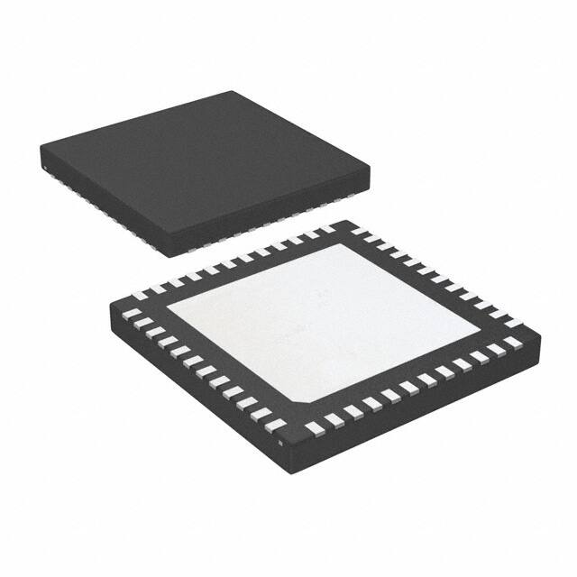


 工商网监
湘ICP备2023018690号
工商网监
湘ICP备2023018690号
