Order
Now
Product
Folder
Support &
Community
Tools &
Software
Technical
Documents
LMK60E2-100M, LMK60E2-125M, LMK60E2-156M, LMK60E0-156M
LMK60E0-212M, LMK60I2-100M, LMK60I2-322M
SNAS718C – DECEMBER 2016 – REVISED DECEMBER 2017
LMK60XX High Performance Low Jitter Oscillator
1 Features
3 Description
•
The LMK60EX is a family of low jitter oscillators that
generate a commonly used reference clock. The
device is pre-programmed in factory to support any
reference clock frequency; supported output formats
are LVPECL, LVDS, and HCSL up to 400 MHz.
Internal power conditioning provide excellent power
supply ripple rejection (PSRR), reducing the cost and
complexity of the power delivery network. The device
operates from a single 3.3-V ±5% supply.
1
•
•
•
•
•
Low Noise, High Performance
– Jitter: 150 fs RMS Typical Fout > 100 MHz
– PSRR: –60 dBc, Robust Supply Noise
Immunity
Supported Output Format
– LVPECL, LVDS and HCSL up to 400 MHz
Total Frequency Tolerance of ±50 ppm
(LMK60X2) and ±25 ppm (LMK60X0)
3.3-V Operating Voltage
Industrial Temperature Range (–40ºC to +85ºC)
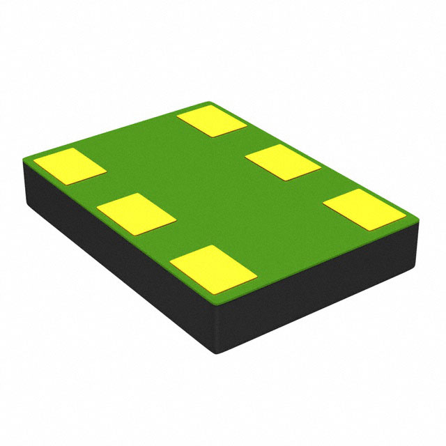
7-mm × 5-mm 6-pin Package That is PinCompatible With Industry Standard 7050 XO
Package
Device Information(1)
PART NUMBER
PACKAGE
SIZE
LMK60E2-100M
QFM (6)
7.00 mm × 5.00 mm
LMK60E2-125M
QFM (6)
7.00 mm × 5.00 mm
LMK60E2-156M
QFM (6)
7.00 mm × 5.00 mm
LMK60E0-156M
QFM (6)
7.00 mm × 5.00 mm
2 Applications
LMK60E0-212M
QFM (6)
7.00 mm × 5.00 mm
•
LMK60I2-100M
QFM (6)
7.00 mm × 5.00 mm
LMK60I2-322M
QFM (6)
7.00 mm × 5.00 mm
•
•
•
•
High-Performance Replacement for Crystal-,
SAW-, or Silicon-Based Oscillators
Switches, Routers, Network Line Cards, Base
Band Units (BBU), Servers, Storage/SAN
Test and Measurement
Medical Imaging
FPGA, Processor Attach
(1) For all available packages, see the orderable addendum at
the end of the data sheet.
Output Frequency Options
OUTPUT FREQ
(MHz) AND FORMAT
TOTAL FREQ
STABILITY (ppm)
LMK60E2-100M
100 LVPECL
±50
LMK60E2-125M
125 LVPECL
±50
LMK60E2-156M
156.25 LVPECL
±50
LMK60E0-156M
156.25 LVPECL
±25
LMK60E0-212M
212.5 LVPECL
±25
LMK60I2-100M
100 HCSL
±50
LMK60I2-322M
322.265625 HCSL
±50
PART NUMBER
Pinout
6
OE
1
6
VDD
NC
2
5
OUTN
GND
3
4
OUTP
1
2
5
4
3
1
An IMPORTANT NOTICE at the end of this data sheet addresses availability, warranty, changes, use in safety-critical applications,
intellectual property matters and other important disclaimers. PRODUCTION DATA.
�LMK60E2-100M, LMK60E2-125M, LMK60E2-156M, LMK60E0-156M
LMK60E0-212M, LMK60I2-100M, LMK60I2-322M
SNAS718C – DECEMBER 2016 – REVISED DECEMBER 2017
www.ti.com
Table of Contents
1
2
3
4
5
6
Features ..................................................................
Applications ...........................................................
Description .............................................................
Revision History.....................................................
Pin Configuration and Functions .........................
Specifications.........................................................
1
1
1
2
3
3
6.1
6.2
6.3
6.4
6.5
6.6
6.7
6.8
6.9
6.10
3
3
4
4
4
4
5
5
5
5
Absolute Maximum Ratings ......................................
ESD Ratings ............................................................
Recommended Operating Conditions.......................
Thermal Information ..................................................
Electrical Characteristics - Power Supply .................
LVPECL Output Characteristics................................
LVDS Output Characteristics ....................................
HCSL Output Characteristics....................................
OE Input Characteristics ...........................................
Frequency Tolerance Characteristics .....................
6.11
6.12
6.13
6.14
Power-On/Reset Characteristics (VDD)..................
PSRR Characteristics .............................................
PLL Clock Output Jitter Characteristics ..................
Additional Reliability and Qualification ....................
6
6
6
6
7
Parameter Measurement Information .................. 7
8
9
Power Supply Recommendations........................ 9
Layout ..................................................................... 9
7.1 Device Output Configurations ................................... 7
9.1 Layout Guidelines ..................................................... 9
10 Device and Documentation Support ................. 11
10.1
10.2
10.3
10.4
10.5
Receiving Notification of Documentation Updates
Community Resources..........................................
Trademarks ...........................................................
Electrostatic Discharge Caution ............................
Glossary ................................................................
11
11
11
11
11
11 Mechanical, Packaging, and Orderable
Information ........................................................... 11
4 Revision History
Changes from Revision B (November 2017) to Revision C
•
Page
New release of LMK60E2-100M............................................................................................................................................. 1
Changes from Revision A (June 2017) to Revision B
Page
•
New release of LMK60E2-125M............................................................................................................................................. 1
•
New release of LMK60I2-100M .............................................................................................................................................. 1
•
New release of LMK60I2-322M ............................................................................................................................................. 1
Changes from Original (December 2016) to Revision A
•
2
Page
Added LMK60E0-156M and LMK60E0-212M ....................................................................................................................... 1
Submit Documentation Feedback
Copyright © 2016–2017, Texas Instruments Incorporated
Product Folder Links: LMK60E2-100M LMK60E2-125M LMK60E2-156M LMK60E0-156M LMK60E0-212M LMK60I2100M LMK60I2-322M
�LMK60E2-100M, LMK60E2-125M, LMK60E2-156M, LMK60E0-156M
LMK60E0-212M, LMK60I2-100M, LMK60I2-322M
www.ti.com
SNAS718C – DECEMBER 2016 – REVISED DECEMBER 2017
5 Pin Configuration and Functions
SIA Package
6-pin QFM
Top View
OE
1
6
VDD
NC
2
5
OUTN
GND
3
4
OUTP
Pin Functions
PIN
NAME
I/O
NO.
DESCRIPTION
POWER
GND
3
Ground
Device ground
VDD
6
Analog
3.3-V power supply
4, 5
Universal
OUTPUT BLOCK
OUTP,
OUTN
Differential output pair (LVPECL, LVDS or HCSL).
DIGITAL CONTROL / INTERFACES
NC
2
N/A
OE
1
LVCMOS
No connect
Output enable (internal pullup). When set to low, output pair is disabled and set at high
impedance.
6 Specifications
6.1 Absolute Maximum Ratings
over operating free-air temperature range (unless otherwise noted) (1)
MIN
MAX
UNIT
VDD
Device supply voltage
–0.3
3.6
V
VIN
Output voltage for logic inputs
–0.3
VDD + 0.3
V
VOUT
Output voltage for clock outputs
–0.3
VDD + 0.3
V
TJ
Junction temperature
150
°C
TSTG
Storage temperature
125
°C
(1)
–40
Stresses beyond those listed under Absolute Maximum Ratings may cause permanent damage to the device. These are stress ratings
only, which do not imply functional operation of the device at these or any other conditions beyond those indicated under Recommended
Operating Conditions. Exposure to absolute maximum-rated conditions for extended periods may affect device reliability.
6.2 ESD Ratings
VALUE
V(ESD)
(1)
(2)
Electrostatic discharge
Human-body model (HBM), per ANSI/ESDA/JEDEC JS-001 (1)
±2000
Charged-device model (CDM), per JEDEC specification JESD22-C101 (2)
±500
UNIT
V
JEDEC document JEP155 states that 500 V HBM allows safe manufacturing with a standard ESD control process.
JEDEC document JEP157 states that 250 V CDM allows safe manufacturing with a standard ESD control process.
Copyright © 2016–2017, Texas Instruments Incorporated
Submit Documentation Feedback
Product Folder Links: LMK60E2-100M LMK60E2-125M LMK60E2-156M LMK60E0-156M LMK60E0-212M LMK60I2100M LMK60I2-322M
3
�LMK60E2-100M, LMK60E2-125M, LMK60E2-156M, LMK60E0-156M
LMK60E0-212M, LMK60I2-100M, LMK60I2-322M
SNAS718C – DECEMBER 2016 – REVISED DECEMBER 2017
www.ti.com
6.3 Recommended Operating Conditions
over operating free-air temperature range (unless otherwise noted)
VDD
Device supply voltage
TA
Ambient temperature
TJ
Junction temperature
tRAMP
VDD power-up ramp time
MIN
NOM
MAX
3.135
3.3
3.465
V
–40
25
85
°C
0.1
UNIT
105
°C
100
ms
6.4 Thermal Information
(2) (3) (4)
LMK60EX
SIA (QFM)
THERMAL METRIC (1)
UNIT
6 PINS
Airflow (LFM) 0
RθJA
Junction-to-ambient thermal resistance
74.8
°C/W
RθJC(top)
Junction-to-case (top) thermal resistance
46.7
°C/W
RθJB
Junction-to-board thermal resistance
49.0
°C/W
ψJT
Junction-to-top characterization parameter
14.8
°C/W
ψJB
Junction-to-board characterization parameter
48.7
°C/W
RθJC(bot)
Junction-to-case (bottom) thermal resistance
n/a
°C/W
(1)
(2)
(3)
(4)
For more information about traditional and new thermal metrics, see the Semiconductor and IC Package Thermal Metrics application
report.
The package thermal resistance is calculated on a 4 layer JEDEC board.
Connected to GND with 2 thermal vias (0.3-mm diameter).
ψJB (junction to board) is used when the main heat flow is from the junction to the GND pad. Please refer to Thermal Considerations
section for more information on ensuring good system reliability and quality.
6.5 Electrical Characteristics - Power Supply (1)
VDD = 3.3 V ± 5%, TA = -40C to 85°C
PARAMETER
IDD
Device current consumption
Device current consumption
when output is disabled
IDD-PD
(1)
(2)
(3)
TEST CONDITIONS
TYP
MAX
LVPECL (2)
MIN
95
110
LVDS
85
100
HCSL (3)
90
105
OE = GND
70
UNIT
mA
mA
Refer to Parameter Measurement Information for relevant test conditions.
On-chip power dissipation should exclude 40 mW, dissipated in the 150 Ω termination resistors, from total power dissipation.
Excludes load current.
6.6 LVPECL Output Characteristics (1)
VDD = 3.3 V ± 5%, TA = -40C to 85°C
PARAMETER
fOUT
Output frequency (2)
VOD
Output voltage swing (VOH – VOL) (2)
VOUT, DIFF, PP
Differential output peak-to-peak swing
VOS
Output common-mode voltage
tR / tF
Output rise/fall time (20% to 80%) (3)
ODC
Output duty cycle (3)
(1)
(2)
(3)
4
TEST CONDITIONS
MIN
TYP
700
950
MAX
UNIT
400
MHz
1200
mV
2 × |VOD|
V
VDD – 1.45
260
45%
V
350
ps
55%
Refer to Parameter Measurement Information for relevant test conditions.
An output frequency over fOUT max spec is possible, but output swing may be less than VOD min spec.
Ensured by characterization.
Submit Documentation Feedback
Copyright © 2016–2017, Texas Instruments Incorporated
Product Folder Links: LMK60E2-100M LMK60E2-125M LMK60E2-156M LMK60E0-156M LMK60E0-212M LMK60I2100M LMK60I2-322M
�LMK60E2-100M, LMK60E2-125M, LMK60E2-156M, LMK60E0-156M
LMK60E0-212M, LMK60I2-100M, LMK60I2-322M
www.ti.com
SNAS718C – DECEMBER 2016 – REVISED DECEMBER 2017
6.7 LVDS Output Characteristics (1)
VDD = 3.3 V ± 5%, TA = -40°C to 85°C
PARAMETER
TEST CONDITIONS
fOUT
Output frequency
VOD
Output voltage swing (VOH – VOL) (1)
VOUT, DIFF, PP
Differential output peak-to-peak swing
VOS
Output common-mode voltage
tR / tF
Output rise/fall time (20% to 80%)
ODC
Output duty cycle (2)
ROUT
Differential output impedance
(1)
(2)
MIN
TYP
300
390
(1)
MAX
UNIT
400
MHz
480
mV
2 x |VOD|
V
1.2
V
(2)
260
350
45%
ps
55%
107
Ω
An output frequency over fOUT max spec is possible, but output swing may be less than VOD min spec.
Ensured by characterization.
6.8 HCSL Output Characteristics (1)
VDD = 3.3 V ± 5%, TA = -40°C to 85°C
PARAMETER
TEST CONDITIONS
MIN
TYP
MAX
UNIT
fOUT
Output frequency
400
MHz
VOH
Output high voltage
660
900
mV
VOL
Output low voltage
–100
100
mV
250
475
mV
0
140
mV
1
3
V/ns
45%
55%
VCROSS
Absolute crossing voltage
(2) (3)
VCROSS-DELTA Variation of VCROSS (2) (3)
dV/dt
Slew rate (4)
ODC
Output duty cycle (4)
(1)
(2)
(3)
(4)
Refer to Parameter Measurement Information for relevant test conditions.
Measured from –150 mV to +150 mV on the differential waveform with the 300 mVpp measurement window centered on the differential
zero crossing.
Ensured by design.
Ensured by characterization.
6.9 OE Input Characteristics
VDD = 3.3 V ± 5%, TA = -40°C to 85°C
PARAMETER
TEST CONDITIONS
MIN
VIH
Input high voltage
VIL
Input low voltage
IIH
Input high current
VIH = VDD
–40
IIL
Input low current
VIL = GND
–40
CIN
Input capacitance
TYP
MAX
UNIT
1.4
V
0.6
V
40
µA
40
µA
2
pF
6.10 Frequency Tolerance Characteristics (1)
VDD = 3.3 V ± 5%, TA = -40°C to 85°C
PARAMETER
fT
(1)
Total frequency tolerance
TEST CONDITIONS
MIN
LMK60X2: All output formats, frequency
bands and device junction temperature up to
105°C; includes initial freq tolerance,
temperature & supply voltage variation, solder
reflow and 5-year aging at 40°C
LMK60X0: All output formats, frequency
bands and device junction temperature up to
105°C; includes initial freq tolerance,
temperature & supply voltage variation, solder
reflow and 5-year aging at 40°C
TYP
MAX
UNIT
–50
50
ppm
–25
25
ppm
Ensured by characterization.
Copyright © 2016–2017, Texas Instruments Incorporated
Submit Documentation Feedback
Product Folder Links: LMK60E2-100M LMK60E2-125M LMK60E2-156M LMK60E0-156M LMK60E0-212M LMK60I2100M LMK60I2-322M
5
�LMK60E2-100M, LMK60E2-125M, LMK60E2-156M, LMK60E0-156M
LMK60E0-212M, LMK60I2-100M, LMK60I2-322M
SNAS718C – DECEMBER 2016 – REVISED DECEMBER 2017
www.ti.com
6.11 Power-On/Reset Characteristics (VDD)
VDD = 3.3 V ± 5%, TA = -40°C to 85°C
PARAMETER
TEST CONDITIONS
MIN
(1)
VTHRESH
Threshold voltage
VDROOP
Allowable voltage droop (2)
(1)
TYP
MAX
2.85
UNIT
3
V
0.1
V
Time elapsed from VDD at 3.135 V to output
enabled
10
ms
tSTARTUP
Start-up time
tOE-EN
Output enable time (2)
Time elapsed from OE at VIH to output enabled
50
µs
tOE-DIS
Output disable time (2)
Time elapsed from OE at VIL to output disabled
50
µs
(1)
(2)
Ensured by characterization.
Ensured by design.
6.12 PSRR Characteristics (1)
VDD = 3.3 V, TA = 25°C
PARAMETER
PSRR
(1)
(2)
(3)
Spurs induced by 50-mV
power supply ripple (2) (3) at
156.25-MHz output, all
output types
TEST CONDITIONS
MIN
TYP
Sine wave at 50 kHz
–60
Sine wave at 100 kHz
–60
Sine wave at 500 kHz
–60
Sine wave at 1 MHz
–60
MAX
UNIT
dBc
Refer to Parameter Measurement Information for relevant test conditions.
Measured max spur level with 50 mVpp sinusoidal signal between 50 kHz and 1 MHz applied on VDD pin
DJSPUR (ps, pk-pk) = [2*10(SPUR/20) / (π*fOUT)]*1e6, where PSRR or SPUR in dBc and fOUT in MHz.
6.13 PLL Clock Output Jitter Characteristics (1) (2)
VDD = 3.3 V ± 5%, TA = -40°C to 85°C
PARAMETER
RJ
(1)
(2)
(3)
RMS phase jitter (3)
(12 kHz – 20 MHz)
TEST CONDITIONS
fOUT ≥ 100 MHz, all output types
MIN
TYP
MAX
UNIT
150
250
fs RMS
Refer to Parameter Measurement Information for relevant test conditions.
Phase jitter measured with Agilent E5052 signal source analyzer using a differential-to-single ended converter (balun or buffer).
Ensured by characterization.
6.14 Additional Reliability and Qualification
6
PARAMETER
CONDITION / TEST METHOD
Mechanical Shock
MIL-STD-202, Method 213
Mechanical Vibration
MIL-STD-202, Method 204
Moisture Sensitivity Level
J-STD-020, MSL3
Submit Documentation Feedback
Copyright © 2016–2017, Texas Instruments Incorporated
Product Folder Links: LMK60E2-100M LMK60E2-125M LMK60E2-156M LMK60E0-156M LMK60E0-212M LMK60I2100M LMK60I2-322M
�LMK60E2-100M, LMK60E2-125M, LMK60E2-156M, LMK60E0-156M
LMK60E0-212M, LMK60I2-100M, LMK60I2-322M
www.ti.com
SNAS718C – DECEMBER 2016 – REVISED DECEMBER 2017
7 Parameter Measurement Information
7.1 Device Output Configurations
High impedance differential probe
LMK60XX
LVPECL
150
Oscilloscope
150
Figure 1. LVPECL Output DC Configuration During Device Test
High impedance differential probe
LMK60XX
LVDS
Oscilloscope
Figure 2. LVDS Output DC Configuration During Device Test
High impedance differential probe
HCSL
LMK60XX
50
Oscilloscope
50
Figure 3. HCSL Output DC Configuration During Device Test
LMK60XX
Balun/
Buffer
LVPECL
150
(1)
Phase Noise/
Spectrum
Analyzer
150
Figure 4. LVPECL Output AC Configuration During Device Test
(1)
Also compatible with 85 Ω termination
Copyright © 2016–2017, Texas Instruments Incorporated
Submit Documentation Feedback
Product Folder Links: LMK60E2-100M LMK60E2-125M LMK60E2-156M LMK60E0-156M LMK60E0-212M LMK60I2100M LMK60I2-322M
7
�LMK60E2-100M, LMK60E2-125M, LMK60E2-156M, LMK60E0-156M
LMK60E0-212M, LMK60I2-100M, LMK60I2-322M
SNAS718C – DECEMBER 2016 – REVISED DECEMBER 2017
www.ti.com
Device Output Configurations (continued)
LMK60XX
Balun/
Buffer
LVDS
Phase Noise/
Spectrum
Analyzer
Figure 5. LVDS Output AC Configuration During Device Test
LMK60XX
Balun/
Buffer
HCSL
50
Phase Noise/
Spectrum
Analyzer
50
Figure 6. HCSL Output AC Configuration During Device Test
Sine wave
Modulator
Power Supply
LMK60XX
Balun
150 (LVPECL)
Open (LVDS)
50 (HCSL)
Phase Noise/
Spectrum
Analyzer
150 (LVPECL)
Open (LVDS)
50 (HCSL)
Figure 7. PSRR Test Setup
OUT_P
VOD
OUT_N
80%
VOUT,DIFF,PP = 2 x VOD
0V
20%
tR
tF
Figure 8. Differential Output Voltage and Rise/Fall Time
8
Submit Documentation Feedback
Copyright © 2016–2017, Texas Instruments Incorporated
Product Folder Links: LMK60E2-100M LMK60E2-125M LMK60E2-156M LMK60E0-156M LMK60E0-212M LMK60I2100M LMK60I2-322M
�LMK60E2-100M, LMK60E2-125M, LMK60E2-156M, LMK60E0-156M
LMK60E0-212M, LMK60I2-100M, LMK60I2-322M
www.ti.com
SNAS718C – DECEMBER 2016 – REVISED DECEMBER 2017
8 Power Supply Recommendations
For best electrical performance of LMK60EX, TI recommends using a combination of 10 µF, 1 µF, and 0.1 µF on
its power-supply bypass network. TI also recommends using component side mounting of the power-supply
bypass capacitors and it is best to use 0201 or 0402 body size capacitors to facilitate signal routing. Keep the
connections between the bypass capacitors and the power supply on the device as short as possible. Ground the
other side of the capacitor using a low impedance connection to the ground plane. Figure 9 shows the layout
recommendation for power supply decoupling of LMK60EX.
9 Layout
9.1 Layout Guidelines
The following sections provides recommendations for board layout, solder reflow profile, and power supply
bypassing when using LMK60EX to ensure good thermal and electrical performance, along with overall signal
integrity of entire system.
9.1.1 Ensuring Thermal Reliability
The LMK60EX is a high-performance device. Therefore, pay careful attention to device configuration and the
printed-circuit board (PCB) layout with respect to power consumption. The ground pin must be connected to the
ground plane of the PCB through three vias or more, as shown in Figure 9, to maximize thermal dissipation out
of the package.
Equation 1 describes the relationship between the PCB temperature around the LMK60EX and its junction
temperature.
TB = TJ – ΨJB * P
where
•
•
•
•
TB: PCB temperature around the LMK60EX
TJ: Junction temperature of LMK60EX
ΨJB: Junction-to-board thermal resistance parameter of LMK60EX (48.7°C/W without airflow)
P: On-chip power dissipation of LMK60EX
(1)
To ensure that the maximum junction temperature of LMK60EX is below 105°C, it can be calculated that the
maximum PCB temperature without airflow should be at 87°C or below when the device is optimized for best
performance resulting in maximum on-chip power dissipation of 0.36 W.
9.1.2 Best Practices for Signal Integrity
For best electrical performance and signal integrity of entire system with LMK60EX, TI recommends routing vias
into decoupling capacitors and then into the LMK60EX. TI also recommends increasing the via count and width
of the traces wherever possible. These steps ensure lowest impedance and shortest path for high frequency
current flow. Figure 9 shows the layout recommendation for LMK60EX.
Copyright © 2016–2017, Texas Instruments Incorporated
Submit Documentation Feedback
Product Folder Links: LMK60E2-100M LMK60E2-125M LMK60E2-156M LMK60E0-156M LMK60E0-212M LMK60I2100M LMK60I2-322M
9
�LMK60E2-100M, LMK60E2-125M, LMK60E2-156M, LMK60E0-156M
LMK60E0-212M, LMK60I2-100M, LMK60I2-322M
SNAS718C – DECEMBER 2016 – REVISED DECEMBER 2017
www.ti.com
Layout Guidelines (continued)
Figure 9. LMK60EX Layout Recommendation for Power Supply and Ground
9.1.3 Recommended Solder Reflow Profile
TI recommends following the recommendations of the solder paste supplier to optimize flux activity and to
achieve proper melting temperatures of the alloy within the guidelines of J-STD-20. Processing the LMK60EX to
be processed with the lowest peak temperature possible while also remaining below the components peak
temperature rating as listed on the MSL label is preferred. The exact temperature profile would depend on
several factors including maximum peak temperature for the component as rated on the MSL label, board
thickness, PCB material type, PCB geometries, component locations, sizes, densities within PCB, as well as the
recommended soldering profile from the manufacturer and capability of the reflow equipment to as confirmed by
the SMT assembly operation.
10
Submit Documentation Feedback
Copyright © 2016–2017, Texas Instruments Incorporated
Product Folder Links: LMK60E2-100M LMK60E2-125M LMK60E2-156M LMK60E0-156M LMK60E0-212M LMK60I2100M LMK60I2-322M
�LMK60E2-100M, LMK60E2-125M, LMK60E2-156M, LMK60E0-156M
LMK60E0-212M, LMK60I2-100M, LMK60I2-322M
www.ti.com
SNAS718C – DECEMBER 2016 – REVISED DECEMBER 2017
10 Device and Documentation Support
10.1 Receiving Notification of Documentation Updates
To receive notification of documentation updates, navigate to the device product folder on ti.com. In the upper
right corner, click on Alert me to register and receive a weekly digest of any product information that has
changed. For change details, review the revision history included in any revised document.
10.2 Community Resources
The following links connect to TI community resources. Linked contents are provided "AS IS" by the respective
contributors. They do not constitute TI specifications and do not necessarily reflect TI's views; see TI's Terms of
Use.
TI E2E™ Online Community TI's Engineer-to-Engineer (E2E) Community. Created to foster collaboration
among engineers. At e2e.ti.com, you can ask questions, share knowledge, explore ideas and help
solve problems with fellow engineers.
Design Support TI's Design Support Quickly find helpful E2E forums along with design support tools and
contact information for technical support.
10.3 Trademarks
E2E is a trademark of Texas Instruments.
All other trademarks are the property of their respective owners.
10.4 Electrostatic Discharge Caution
These devices have limited built-in ESD protection. The leads should be shorted together or the device placed in conductive foam
during storage or handling to prevent electrostatic damage to the MOS gates.
10.5 Glossary
SLYZ022 — TI Glossary.
This glossary lists and explains terms, acronyms, and definitions.
11 Mechanical, Packaging, and Orderable Information
The following pages include mechanical, packaging, and orderable information. This information is the most
current data available for the designated devices. This data is subject to change without notice and revision of
this document. For browser-based versions of this data sheet, refer to the left-hand navigation.
Copyright © 2016–2017, Texas Instruments Incorporated
Submit Documentation Feedback
Product Folder Links: LMK60E2-100M LMK60E2-125M LMK60E2-156M LMK60E0-156M LMK60E0-212M LMK60I2100M LMK60I2-322M
11
�LMK60E2-100M, LMK60E2-125M, LMK60E2-156M, LMK60E0-156M
LMK60E0-212M, LMK60I2-100M, LMK60I2-322M
SNAS718C – DECEMBER 2016 – REVISED DECEMBER 2017
www.ti.com
PACKAGE OUTLINE
SIA0006A
QFM - 1.15 mm max height
SCALE 2.200
QUAD FLAT MODULE
5.1
4.9
A
B
PIN 1 INDEX
AREA
7.1
6.9
C
1.15 MAX
0.1 C
3X 3.7
6X (0.15)
3
4
4X (0.26)
SYMM
2X
5.08
4X
2.54
6X
0.1
0.05
6
1
SYMM
1.43
1.37
6X
C A
C
B
1.03
0.97
4222361/B 10/2015
NOTES:
1. All linear dimensions are in millimeters. Any dimensions in parenthesis are for reference only. Dimensioning and tolerancing
per ASME Y14.5M.
2. This drawing is subject to change without notice.
www.ti.com
12
Submit Documentation Feedback
Copyright © 2016–2017, Texas Instruments Incorporated
Product Folder Links: LMK60E2-100M LMK60E2-125M LMK60E2-156M LMK60E0-156M LMK60E0-212M LMK60I2100M LMK60I2-322M
�LMK60E2-100M, LMK60E2-125M, LMK60E2-156M, LMK60E0-156M
LMK60E0-212M, LMK60I2-100M, LMK60I2-322M
www.ti.com
SNAS718C – DECEMBER 2016 – REVISED DECEMBER 2017
EXAMPLE BOARD LAYOUT
SIA0006A
QFM - 1.15 mm max height
QUAD FLAT MODULE
SYMM
6X (1)
1
6
6X (1.4)
SYMM
4X (2.54)
4
3
(R0.05) TYP
(3.7)
LAND PATTERN EXAMPLE
1:1 RATIO WITH PACKAGE SOLDER PADS
SCALE:8X
0.07 MIN
ALL AROUND
METAL
SOLDER MASK
OPENING
SOLDER MASK
OPENING
METAL UNDER
SOLDER MASK
SOLDER MASK
DEFINED
NON SOLDER MASK
DEFINED
SOLDER MASK DETAILS
NOT TO SCALE
4222361/B 10/2015
NOTES: (continued)
3. For more information, see Texas Instruments literature number SLUA271 (www.ti.com/lit/slua271).
www.ti.com
Copyright © 2016–2017, Texas Instruments Incorporated
Submit Documentation Feedback
Product Folder Links: LMK60E2-100M LMK60E2-125M LMK60E2-156M LMK60E0-156M LMK60E0-212M LMK60I2100M LMK60I2-322M
13
�LMK60E2-100M, LMK60E2-125M, LMK60E2-156M, LMK60E0-156M
LMK60E0-212M, LMK60I2-100M, LMK60I2-322M
SNAS718C – DECEMBER 2016 – REVISED DECEMBER 2017
www.ti.com
EXAMPLE STENCIL DESIGN
SIA0006A
QFM - 1.15 mm max height
QUAD FLAT MODULE
SYMM
12X (1)
1
6
12X (0.6)
METAL TYP
(R0.05)
SYMM
4X (2.54)
4
3
(0.4) TYP
(3.7)
SOLDER PASTE EXAMPLE
BASED ON 0.125 mm THICK STENCIL
PRINTED SOLDER COVERAGE BY AREA
ALL PADS: 86%
SCALE:10X
4222361/B 10/2015
NOTES: (continued)
4. Laser cutting apertures with trapezoidal walls and rounded corners may offer better paste release. IPC-7525 may have alternate
design recommendations.
www.ti.com
14
Submit Documentation Feedback
Copyright © 2016–2017, Texas Instruments Incorporated
Product Folder Links: LMK60E2-100M LMK60E2-125M LMK60E2-156M LMK60E0-156M LMK60E0-212M LMK60I2100M LMK60I2-322M
�PACKAGE OPTION ADDENDUM
www.ti.com
10-Dec-2020
PACKAGING INFORMATION
Orderable Device
Status
(1)
Package Type Package Pins Package
Drawing
Qty
Eco Plan
(2)
Lead finish/
Ball material
MSL Peak Temp
Op Temp (°C)
Device Marking
(3)
(4/5)
(6)
LMK60E0-156M25SIAR
ACTIVE
QFM
SIA
6
2500
RoHS & Green
NIAU
Level-3-260C-168 HR
-40 to 85
LMK60E0
156M25
LMK60E0-156M25SIAT
ACTIVE
QFM
SIA
6
250
RoHS & Green
NIAU
Level-3-260C-168 HR
-40 to 85
LMK60E0
156M25
LMK60E0-212M50SIAR
ACTIVE
QFM
SIA
6
2500
RoHS & Green
NIAU
Level-3-260C-168 HR
-40 to 85
LMK60E0
212M50
LMK60E0-212M50SIAT
ACTIVE
QFM
SIA
6
250
RoHS & Green
NIAU
Level-3-260C-168 HR
-40 to 85
LMK60E0
212M50
LMK60E2-100M00SIAR
ACTIVE
QFM
SIA
6
2500
RoHS & Green
NIAU
Level-3-260C-168 HR
-40 to 85
LMK60E2
100M00
LMK60E2-100M00SIAT
ACTIVE
QFM
SIA
6
250
RoHS & Green
NIAU
Level-3-260C-168 HR
-40 to 85
LMK60E2
100M00
LMK60E2-125M00SIAR
ACTIVE
QFM
SIA
6
2500
RoHS & Green
NIAU
Level-3-260C-168 HR
-40 to 85
LMK60E2
125M00
LMK60E2-125M00SIAT
ACTIVE
QFM
SIA
6
250
RoHS & Green
NIAU
Level-3-260C-168 HR
-40 to 85
LMK60E2
125M00
LMK60E2-156M25SIAR
ACTIVE
QFM
SIA
6
2500
RoHS & Green
NIAU
Level-3-260C-168 HR
-40 to 85
LMK60E2
156M25
LMK60E2-156M25SIAT
ACTIVE
QFM
SIA
6
250
RoHS & Green
NIAU
Level-3-260C-168 HR
-40 to 85
LMK60E2
156M25
LMK60I2-100M00SIAR
ACTIVE
QFM
SIA
6
2500
RoHS & Green
NIAU
Level-3-260C-168 HR
-40 to 85
LMK60I2
100M00
LMK60I2-100M00SIAT
ACTIVE
QFM
SIA
6
250
RoHS & Green
NIAU
Level-3-260C-168 HR
-40 to 85
LMK60I2
100M00
LMK60I2-322M26SIAR
ACTIVE
QFM
SIA
6
2500
RoHS & Green
NIAU
Level-3-260C-168 HR
-40 to 85
LMK60I2
322M26
LMK60I2-322M26SIAT
ACTIVE
QFM
SIA
6
250
RoHS & Green
NIAU
Level-3-260C-168 HR
-40 to 85
LMK60I2
322M26
(1)
The marketing status values are defined as follows:
ACTIVE: Product device recommended for new designs.
LIFEBUY: TI has announced that the device will be discontinued, and a lifetime-buy period is in effect.
NRND: Not recommended for new designs. Device is in production to support existing customers, but TI does not recommend using this part in a new design.
PREVIEW: Device has been announced but is not in production. Samples may or may not be available.
OBSOLETE: TI has discontinued the production of the device.
Addendum-Page 1
Samples
�PACKAGE OPTION ADDENDUM
www.ti.com
10-Dec-2020
(2)
RoHS: TI defines "RoHS" to mean semiconductor products that are compliant with the current EU RoHS requirements for all 10 RoHS substances, including the requirement that RoHS substance
do not exceed 0.1% by weight in homogeneous materials. Where designed to be soldered at high temperatures, "RoHS" products are suitable for use in specified lead-free processes. TI may
reference these types of products as "Pb-Free".
RoHS Exempt: TI defines "RoHS Exempt" to mean products that contain lead but are compliant with EU RoHS pursuant to a specific EU RoHS exemption.
Green: TI defines "Green" to mean the content of Chlorine (Cl) and Bromine (Br) based flame retardants meet JS709B low halogen requirements of


 工商网监
湘ICP备2023018690号
工商网监
湘ICP备2023018690号
