www.ti.com
Table of Contents
User’s Guide
LMX2594 EVM Instructions – 15-GHz Wideband Low Noise
PLL With Integrated VCO
Noel Fung, Julian Di Matteo
ABSTRACT
This Evaluation Module is for the LMX2594, which is the first PLL with integrated VCO in industry to get
fundamental VCO output up to 15 GHz. The industry leading PLL FOM is –236 dBc/Hz with 1/f of –129 dBc/Hz.
This device supports the JESD204B standard (as in the LMX2594 can generate or repeat the SYSREF signal),
and is designed for clock high-speed data converters. The integrated jitter from the EVM measurements is less
than 50 fs at 9-GHz carrier frequency. By providing a SYNC signal, the user can synchronize the output phase
across multiple LMX2594 devices. The LMX2594 can also generate a frequency ramp as demonstrated in this
evaluation module. With an on-board oscillator, the setup process only requires a 3.3-V power supply and a
Reference Pro module (included for SPI Programming interface). The software is simple with an intuitive and
user-friendly GUI.
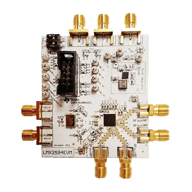
Figure 1-1. LMX2594EVM
Table of Contents
1 Evaluation Board Setup......................................................................................................................................................... 3
2 EVM Description..................................................................................................................................................................... 3
SNAU210B – MARCH 2020 – REVISED JULY 2021
Submit Document Feedback
LMX2594 EVM Instructions – 15-GHz Wideband Low Noise PLL With
Integrated VCO
Copyright © 2021 Texas Instruments Incorporated
1
�Trademarks
www.ti.com
2.1 Installing the Software........................................................................................................................................................4
3 Bringing LMX2594 to a Lock State........................................................................................................................................5
4 Loop Filter Configuration.......................................................................................................................................................5
5 Key Results to Expect............................................................................................................................................................ 6
A Schematic............................................................................................................................................................................... 7
B Bill of Materials.......................................................................................................................................................................8
C Board Layers Stack-Up..........................................................................................................................................................9
D Changing Reference Oscillator and Setup.........................................................................................................................11
E Connecting Reference Pro.................................................................................................................................................. 12
F Ramping Feature.................................................................................................................................................................. 14
G SYSREF Feature...................................................................................................................................................................15
H Enabling Onboard DC-DC Buck Converter (TPS62150)................................................................................................... 16
Revision History.......................................................................................................................................................................16
List of Figures
Figure 1-1. LMX2594EVM........................................................................................................................................................... 1
Figure 1-1. LMX2594EVM Setup.................................................................................................................................................3
Figure 2-1. LMX2594EVM Description........................................................................................................................................ 3
Figure 2-2. Search for LMX2594 on TICS Pro.............................................................................................................................4
Figure 2-3. USB Communications on TICS Pro.......................................................................................................................... 4
Figure 2-4. USB Communication Between TICS Pro and Reference Pro................................................................................... 4
Figure 3-1. TICS Pro GUI LMX2594 Default Configuration......................................................................................................... 5
Figure 4-1. Loop Filter Configuration........................................................................................................................................... 6
Figure 5-1. Phase Noise Plot at 14-GHz Output Frequency........................................................................................................6
Figure A-1. Schematic................................................................................................................................................................. 7
Figure C-1. Board Layer Stack-Up.............................................................................................................................................. 9
Figure C-2. Top Layer.................................................................................................................................................................. 9
Figure C-3. GND Layer................................................................................................................................................................9
Figure C-4. Power Layer............................................................................................................................................................10
Figure C-5. Bottom Layer.......................................................................................................................................................... 10
Figure E-1. LMX2594EVM Setup With Reference Pro.............................................................................................................. 12
Figure E-2. LMK61PD0A2 Output Termination..........................................................................................................................13
Figure F-1. Ramping Example...................................................................................................................................................14
Figure F-2. Ramping Example...................................................................................................................................................14
Figure G-1. SYSREF Example.................................................................................................................................................. 15
Figure H-1. Resistor Configuration to Enable DC-DC............................................................................................................... 16
List of Tables
Table 2-1. Serial Interface Connector Description....................................................................................................................... 4
Table 4-1. Loop Filter Configuration.............................................................................................................................................5
Table B-1. Bill of Materials........................................................................................................................................................... 8
Table D-1. Reference Oscillator Requirements..........................................................................................................................11
Table D-2. Reference Clock Input Configuration........................................................................................................................11
Table E-1. Output Frequency of LMK61PD0A2 (Reference Pro).............................................................................................. 12
Table E-2. Output Type of LMK61PD0A2 (Reference Pro)........................................................................................................12
Table E-3. Output Termination Schemes................................................................................................................................... 13
Table G-1. SYSREF Modes....................................................................................................................................................... 15
Trademarks
PLLATINUM™ is a trademark of Texas Instruments.
All trademarks are the property of their respective owners.
2
LMX2594 EVM Instructions – 15-GHz Wideband Low Noise PLL With
Integrated VCO
Copyright © 2021 Texas Instruments Incorporated
SNAU210B – MARCH 2020 – REVISED JULY 2021
Submit Document Feedback
�www.ti.com
Evaluation Board Setup
1 Evaluation Board Setup
Reference Pro
board
Clean 100 MHz
clock source
3.3 V supply
LMX2594EVM
board
Connect to
a PC
RFoutAP
Connect to
an analyzer
oth
ect b e
Connl interfac
seria gether
to
OSCinM can be left
open
(Optional)
Add a XO here
50
termination
Figure 1-1. LMX2594EVM Setup
1. Power:
a. Set power supply to 3.3 V with 600-mA current limit and connect to VCC SMA.
2. Input Signal:
a. Connect a clean 100-MHz clock source to the OSCinP SMA.
3. Programming Interface:
• Reference Pro will provide SPI interface to program LMX2594.
a. Connect USB cable from laptop or PC to USB port in Reference Pro. This provides power to Reference
Pro board and communication with TICS GUI.
b. Connect 10 pin ribbon cable from Reference Pro to LMX2594EVM as shown above.
4. Output:
a. Connect RFoutAM or RFoutAP to a phase noise analyzer. Connect a 50-Ω resistor on the unused pin if
you are using a single-ended output. Use a balun if you are using a differential output.
2 EVM Description
The LMX2594 is populated on a 4-layer PCB. This brief description should help you use the EVM:
Power supply
3.3 Volt
Loop filter
components
(*_LF)
Diff. RF
Output A
Diff. RF
Output B
SYNC
Serial Interface Pin-out
SYSREF
2
4
6
8
10
1
3
5
7
9
LMX2594
1: SPI read block
2: Lock indicator
Upper position = ON
Lower position = OFF
Lock
indicator
LED
Reference input
SE or Diff
Figure 2-1. LMX2594EVM Description
SNAU210B – MARCH 2020 – REVISED JULY 2021
Submit Document Feedback
LMX2594 EVM Instructions – 15-GHz Wideband Low Noise PLL With
Integrated VCO
Copyright © 2021 Texas Instruments Incorporated
3
�EVM Description
www.ti.com
The serial interface pin description is shown in Table 2-1.
Table 2-1. Serial Interface Connector Description
NO.
NAME
1
RAMPDIR and CE (Choose with Resistors on
Board)
2
CSB
3
MUXout
4
SDI
5
Not Used
6
GND
7
RampCLK
8
SCK
9
SysRefReq
10
SYNC
2.1 Installing the Software
1. Download TICS Pro from the TI Website at www.ti.com/tool/TICSPRO-SW.
2. Install the software by following the wizard.
3. Search for the LMX2594. In the menu bar, search Select Device → PLL + VCO → LMX2594
Figure 2-2. Search for LMX2594 on TICS Pro
4. You are now ready to use this software. Verify that you can communicate with Reference Pro. Select
Interface under USB communications.
Figure 2-3. USB Communications on TICS Pro
5. Click on Identify and you will see the LED (MSP430 Supplied) blinks on Reference Pro.
Figure 2-4. USB Communication Between TICS Pro and Reference Pro
4
LMX2594 EVM Instructions – 15-GHz Wideband Low Noise PLL With
Integrated VCO
Copyright © 2021 Texas Instruments Incorporated
SNAU210B – MARCH 2020 – REVISED JULY 2021
Submit Document Feedback
�www.ti.com
Bringing LMX2594 to a Lock State
3 Bringing LMX2594 to a Lock State
1. Load the default mode by clicking on Default configuration → Default Mode xxxx-xx-xx.
2. From the menu bar, select USB communications → Write All Registers, to write all the registers to LMX2594.
Figure 3-1. TICS Pro GUI LMX2594 Default Configuration
4 Loop Filter Configuration
The parameters for the loop filters are:
Table 4-1. Loop Filter Configuration
PARAMETER
VALUE
VCO Gain
132 MHz/V
Loop Bandwidth
285 kHz
Phase Margin
65 deg
C1_LF
390 pF
C2_LF
68 nF
C3_LF
Open
C4_LF
1800 pF
R2
68 Ω
R3_LF
0Ω
R4_LF
18 Ω
Effective Charge Pump Gain
15 mA
Phase Detector Frequency (MHz)
200 MHz
VCO Frequency
Designed for 15 GHz, but works
over the whole frequency range
SNAU210B – MARCH 2020 – REVISED JULY 2021
Submit Document Feedback
LMX2594 EVM Instructions – 15-GHz Wideband Low Noise PLL With
Integrated VCO
Copyright © 2021 Texas Instruments Incorporated
5
�Key Results to Expect
www.ti.com
Figure 4-1. Loop Filter Configuration
For detailed design and simulation of TI's PLLATINUM™ integrated circuits, see the PLLatinum Sim Tool.
For application notes, blogs, or videos on TI PLL products, see http://www.ti.com/pll.
5 Key Results to Expect
Figure 5-1. Phase Noise Plot at 14-GHz Output Frequency
This assumes that the input reference is very clean, such as a 100-MHz Wenzel oscillator. A signal generator is
NOT sufficiently clean.
6
LMX2594 EVM Instructions – 15-GHz Wideband Low Noise PLL With
Integrated VCO
Copyright © 2021 Texas Instruments Incorporated
SNAU210B – MARCH 2020 – REVISED JULY 2021
Submit Document Feedback
�www.ti.com
Schematic
A Schematic
Figure A-1. Schematic
SNAU210B – MARCH 2020 – REVISED JULY 2021
Submit Document Feedback
LMX2594 EVM Instructions – 15-GHz Wideband Low Noise PLL With
Integrated VCO
Copyright © 2021 Texas Instruments Incorporated
7
�Bill of Materials
www.ti.com
B Bill of Materials
Table B-1. Bill of Materials
8
DESIGNATOR
DESCRIPTION
MANUFACTURER
PART NUMBER
QUANTITY
C1, C3, C9, C14, C15, C17, C30
CAP, CERM, 0.1 µF, 16 V, ±5%, X7R, 0603
AVX
0603YC104JAT2A
7
C1_LF
CAP, CERM, 390 pF, 50 V, ±5%, C0G/NP0,
0603
Kemet
C0603C391J5GACTU
1
C2, C4, C8, C16
CAP, CERM, 10 µF, 10 V, ±10%, X5R, 0805
Kemet
C0805C106K8PACTU
4
C2_LF
CAP, CERM, 0.068 µF, 50 V, ±10%, X7R, 0603
MuRata
GRM188R71H683KA93D
1
C4_LF
CAP, CERM, 1800 pF, 50 V, ±5%, C0G/NP0,
0603
MuRata
GRM1885C1H182JA01D
1
C5, C6, C7, C10, C11, C12
CAP, CERM, 0.01 µF, 16 V, ±10%, X7R, 0402
AT Ceramics
520L103KT16T
6
C18, C23, C24, C26, C27, C28, C29
CAP, CERM, 1 µF, 16 V, ±10%, X7R, 0603
TDK
C1608X7R1C105K080AC
7
C19, C20, C21, C22, C25
CAP, CERM, 10 µF, 10 V, ±20%, X5R, 0603
TDK
C1608X5R1A106M080AC
5
CE_TP, CSB_TP, GND_TP, MUXout_TP,
RampCLK_TP, RampDIR_TP, SCK_TP,
SDI_TP, SYNC_TP, SysRefReq_TP, Vcc_TP,
VccRF_TP, Vtune_TP
Test Point, Compact, White, TH
Keystone
5007
13
Cin_0
CAP, CERM, 10 µF, 25 V, ±10%, X5R, 0805
MuRata
GRM219R61E106KA12D
1
Cout0
CAP, CERM, 22 µF, 16 V, ±10%, X5R, 0805
TDK
C2012X5R1C226K125AC
1
Css
CAP, CERM, 3300 pF, 50 V, ±5%, C0G/NP0,
0603
MuRata
GRM1885C1H332JA01D
1
D1
LED, Green, SMD
Lite-On
LTST-C190GKT
1
L1, L2
Inductor, Multilayer, Air Core, 18 nH, 0.3 A,
0.36 Ω, SMD
MuRata
LQG15HS18NJ02D
2
L1_TPS
Inductor, Shielded, Composite, 2.2 µH, 3.7 A,
0.02 Ω, SMD
Coilcraft
XFL4020-222MEB
1
MUXout_SW
Switch, SPST, Slide, Off-On, 2 Pos, 0.1 A, 20 V,
SMD
CTS Electrocomponents
219-2MST
1
OSCinM, OSCinP, SYNC, SysRef, Vcc
Connector, SMT, End launch SMA 50 ohm
Emerson Network Power
Connectivity
142-0701-851
5
R1
RES, 330 Ω, 5%, 0.1 W, 0603
Yageo America
RC0603JR-07330RL
1
R2
RES, 100 k, 5%, 0.1 W, 0603
Vishay-Dale
CRCW0603100KJNEA
1
R2_LF
RES, 68, 5%, 0.1 W, 0603
Vishay-Dale
CRCW060368R0JNEA
1
R3_LF, R12, R15, R24, R26, R25, R30, R31,
R34, R35, R36, R41, R42, R43, R44, R45
RES, 0, 5%, 0.1 W, 0603
Vishay-Dale
CRCW06030000Z0EA
16
R4_LF
RES, 18, 5%, 0.1 W, 0603
Vishay-Dale
CRCW060318R0JNEA
1
R5, R7, R8, R9, R16, R19, R20, R22
RES, 12 kΩ, 5%, 0.1 W, 0603
Vishay-Dale
CRCW060312K0JNEA
8
R37, R38, R39, R40
RES, 50, 0.1%, 0.05 W, 0402
Vishay-Dale
FC0402E50R0BST1
4
Rfbb1
RES, 180 k, 0.1%, 0.1 W, 0603
Yageo America
RT0603BRD07180KL
1
Rfbt1
RES, 562 k, 1%, 0.1 W, 0603
Vishay-Dale
CRCW0603562KFKEA
1
RFoutAM, RFoutAP, RFoutBM, RFoutBP
JACK, SMA, 50 Ω, Gold, Edge Mount
Johnson
142-0771-831
4
U1
Wideband RF Synthesizer
Texas Instruments
LMX2594RHAR
1
uWire
Header (shrouded), 100 mil, 5x2, Gold plated,
SMD
FCI
52601-S10-8LF
1
LMX2594 EVM Instructions – 15-GHz Wideband Low Noise PLL With
Integrated VCO
Copyright © 2021 Texas Instruments Incorporated
SNAU210B – MARCH 2020 – REVISED JULY 2021
Submit Document Feedback
�www.ti.com
Board Layers Stack-Up
C Board Layers Stack-Up
Top layer
RO4003 (Er = 3.38)
16 mil
GND layer
FR4 (Er = 4.6)
Power layer
62 mil
The top layer is 1-oz. copper.
FR4 (Er = 4.6)
Bottom layer
Figure C-1. Board Layer Stack-Up
Figure C-2. Top Layer
Figure C-3. GND Layer
SNAU210B – MARCH 2020 – REVISED JULY 2021
Submit Document Feedback
LMX2594 EVM Instructions – 15-GHz Wideband Low Noise PLL With
Integrated VCO
Copyright © 2021 Texas Instruments Incorporated
9
�Board Layers Stack-Up
www.ti.com
Figure C-4. Power Layer
Figure C-5. Bottom Layer
10
LMX2594 EVM Instructions – 15-GHz Wideband Low Noise PLL With
Integrated VCO
Copyright © 2021 Texas Instruments Incorporated
SNAU210B – MARCH 2020 – REVISED JULY 2021
Submit Document Feedback
�www.ti.com
Changing Reference Oscillator and Setup
D Changing Reference Oscillator and Setup
The reference can be single-ended or differential. To measure the performance of the PLL ONLY, the
reference should have at least this level of performance. We understand that this can be a challenge at
100-Hz offset:
Table D-1. Reference Oscillator Requirements
100-MHz REFERENCE MINIMUM REQUIREMENTS FOR A 0.4-dB IMPACT ON PLL INBAND PN(1)
(1)
Offset [Hz]
100
1k
10k
100k
Noise level [dBc/Hz]
–139
–149
–159
–164
A noise source 10 dB down from the PLL noise will contribute to raise the noise by 0.4 dB.
There are different options to provide a reference oscillator to LMX2594. Use on-board oscillator, enable
LMK61xx from Reference Pro PCB, or use external oscillator. By default, the EVM is configured for an external
single-ended clock.
Table D-2. Reference Clock Input Configuration
INPUT
EXTERNAL CLOCK
CRYSTAL OSCILLATOR
Singleended
Differential
(LVDS)
SNAU210B – MARCH 2020 – REVISED JULY 2021
Submit Document Feedback
LMX2594 EVM Instructions – 15-GHz Wideband Low Noise PLL With
Integrated VCO
Copyright © 2021 Texas Instruments Incorporated
11
�Connecting Reference Pro
www.ti.com
E Connecting Reference Pro
To use Reference Pro, change the configuration for SE or differential connection as shown on Appendix D.
Figure E-1. LMX2594EVM Setup With Reference Pro
The LMK61PD0A2 has several control pins dedicated for output format control, output frequency control, and
output enable control. These control pins can be configured through the jumpers shown in Table E-1 and Table
E-2.
Jumpers FS1, FS0, OS, and OE can be used to configure the corresponding control pin to either high or low
state by strapping the center pin to VDD position (tie pins 2-3) or GND position (tie pins 1-2), respectively.
Connections from the VDD position to the device supply or from the GND position to the ground plane are
connected by 1.5-kΩ resistors.
Table E-1. Output Frequency of LMK61PD0A2 (Reference Pro)
FS1
FS0
OUTPUT FREQUENCY (MHz)
0
0
100
0
NC
312.5
0
1
125
NC
0
106.25
NC
NC
156.25
NC
1
212.5
1
0
62.5
Table E-2. Output Type of LMK61PD0A2 (Reference Pro)
OS
OE
OUTPUT TYPE
X
O
Disabled (PLL Functional)
0
1
LVPECL
NC
1
LVDS
1
1
HCSL
The OS pin is used to bias internal drivers and change the output type. It is imperative to match the output
termination passive components as shown on Table E-3 with the output type from Table E-2.
12
LMX2594 EVM Instructions – 15-GHz Wideband Low Noise PLL With
Integrated VCO
Copyright © 2021 Texas Instruments Incorporated
SNAU210B – MARCH 2020 – REVISED JULY 2021
Submit Document Feedback
�www.ti.com
Connecting Reference Pro
Table E-3 lists component values for each configuration.
Table E-3. Output Termination Schemes
OUTPUT FORMAT
COUPLING
COMPONENT
VALUE
LVPECL
AC
(default EVM configuration)
R25, R28
0Ω
R26, R29
150 Ω
C24, C25
0.01 µF
R27, R30, R31
DNP
R25, R28, C24, C25
0Ω
R26, R29, R27, R30, R31
DNP
R25, R28, R27, R30
0Ω
R31
100 Ω
C24, C25
0.01 µF
R26, R29
DNP
R25, R27, R28, R30, C24, C25
0Ω
R31
100 Ω
R26, R29
DNP
R25, R28
0Ω
R26, R29
50 Ω
C24, C25
0Ω
R27, R30, R31
DNP
R25, R28
0Ω
R26, R29
50 Ω
C24, C25
0.01 µF
R27. R30, R31
DNP
DC(1)
LVDS(2)
AC
DC
HCSL
AC
DC
(1)
(2)
50 Ω to VCC – 2-V termination is required on receiver.
100-Ω differential termination (R31) is provided on Reference Pro PCB. Removing the differential termination on the EVM is possible if
the differential termination is available on the receiver.
Figure E-2. LMK61PD0A2 Output Termination
SNAU210B – MARCH 2020 – REVISED JULY 2021
Submit Document Feedback
LMX2594 EVM Instructions – 15-GHz Wideband Low Noise PLL With
Integrated VCO
Copyright © 2021 Texas Instruments Incorporated
13
�Ramping Feature
www.ti.com
F Ramping Feature
VCO is ramping from 12 to 12.125 GHz. This can be set up on the ramp GUI tab.
Figure F-1. Ramping Example
Figure F-2. Ramping Example
14
LMX2594 EVM Instructions – 15-GHz Wideband Low Noise PLL With
Integrated VCO
Copyright © 2021 Texas Instruments Incorporated
SNAU210B – MARCH 2020 – REVISED JULY 2021
Submit Document Feedback
�www.ti.com
SYSREF Feature
G SYSREF Feature
1. Configure TICS Pro PLL tab for SYSREF.
• Check the SYSREF_EN box and VCO_PHASE_SYNC box.
• Change OUTB_MUX to SysRef and uncheck the OUT_PD box.
• Confirm the Interpolator frequency is between 800 MHz and 1500 MHz. If not, change the
SYSREF_DIV_PRE drop-down to Div2 or Div4.
• To modify SYSREF frequency, change the value in the SYSREF_DIV box.
• Go to User Controls in the side bar, make sure the INPIN_IGNORE box is unchecked.
2. Click the Toggle SysRefReq Pin box to initiate SYSREF.
Figure G-1. SYSREF Example
Table G-1. SYSREF Modes
MODE NAME
Master Continuos
Master - Pulse
Repeater
DESCRIPTION
TICS PRO - SYS REF SETTINGS
LMX2594 generates SysRef pulses as long as SysRefReq
Default mode. See quick start instructions
pin is held high.
LMX2594 generates a finite number of pulses as long as
the SysRefReq pin is held high. Note: SysRefReq must
be held high for the duration of the pulses.
RFOUTB will repeat external input to SysRefReq pin.
Output will be reclocked to LMX2594 internal frequency
SNAU210B – MARCH 2020 – REVISED JULY 2021
Submit Document Feedback
•
Uncheck SysRefReq under Pins in User Controls tab
•
Check SYSREF_PULSE
•
Set SYSREF_PULSE_CNT to desired number of pulses
•
Check SysRefReq under Pins in User Controls tab
•
Uncheck SysRefReq
•
Check SysRef_Repeat
LMX2594 EVM Instructions – 15-GHz Wideband Low Noise PLL With
Integrated VCO
Copyright © 2021 Texas Instruments Incorporated
15
�Enabling Onboard DC-DC Buck Converter (TPS62150)
www.ti.com
H Enabling Onboard DC-DC Buck Converter (TPS62150)
Figure H-1. Resistor Configuration to Enable DC-DC
1.
2.
3.
4.
MUST SWITCH R35 to Rtps1
MUST SWITCH R34 to Rtps2
Populate Rtps
DC-DC circuitry was optimized for efficiency for 5 to 8 V, but a voltage of 3.3 V to 17 V can be applied to
VCC SMA after resistor network is configured correctly from steps above.
Revision History
NOTE: Page numbers for previous revisions may differ from page numbers in the current version.
Changes from Revision A (March 2020) to Revision B (July 2021)
Page
• Updated the numbering format for tables, figures and cross-references throughout the document...................3
16
LMX2594 EVM Instructions – 15-GHz Wideband Low Noise PLL With
Integrated VCO
Copyright © 2021 Texas Instruments Incorporated
SNAU210B – MARCH 2020 – REVISED JULY 2021
Submit Document Feedback
�IMPORTANT NOTICE AND DISCLAIMER
TI PROVIDES TECHNICAL AND RELIABILITY DATA (INCLUDING DATA SHEETS), DESIGN RESOURCES (INCLUDING REFERENCE
DESIGNS), APPLICATION OR OTHER DESIGN ADVICE, WEB TOOLS, SAFETY INFORMATION, AND OTHER RESOURCES “AS IS”
AND WITH ALL FAULTS, AND DISCLAIMS ALL WARRANTIES, EXPRESS AND IMPLIED, INCLUDING WITHOUT LIMITATION ANY
IMPLIED WARRANTIES OF MERCHANTABILITY, FITNESS FOR A PARTICULAR PURPOSE OR NON-INFRINGEMENT OF THIRD
PARTY INTELLECTUAL PROPERTY RIGHTS.
These resources are intended for skilled developers designing with TI products. You are solely responsible for (1) selecting the appropriate
TI products for your application, (2) designing, validating and testing your application, and (3) ensuring your application meets applicable
standards, and any other safety, security, regulatory or other requirements.
These resources are subject to change without notice. TI grants you permission to use these resources only for development of an
application that uses the TI products described in the resource. Other reproduction and display of these resources is prohibited. No license
is granted to any other TI intellectual property right or to any third party intellectual property right. TI disclaims responsibility for, and you
will fully indemnify TI and its representatives against, any claims, damages, costs, losses, and liabilities arising out of your use of these
resources.
TI’s products are provided subject to TI’s Terms of Sale or other applicable terms available either on ti.com or provided in conjunction with
such TI products. TI’s provision of these resources does not expand or otherwise alter TI’s applicable warranties or warranty disclaimers for
TI products.
TI objects to and rejects any additional or different terms you may have proposed. IMPORTANT NOTICE
Mailing Address: Texas Instruments, Post Office Box 655303, Dallas, Texas 75265
Copyright © 2022, Texas Instruments Incorporated
�