LP395
www.ti.com
SNOSBF3C – APRIL 1998 – REVISED MARCH 2013
LP395 Ultra Reliable Power Transistor
Check for Samples: LP395
FEATURES
1
•
•
•
•
•
•
•
2
Internal Thermal Limiting
Internal Current and Power Limiting
Specified 100 mA Output Current
0.5 μA Typical Base Current
Directly Interfaces with TTL or CMOS
+36 Volts On Base Causes No Damage
2 μs Switching Time
DESCRIPTION
The LP395 is a fast monolithic transistor with
complete overload protection. This very high gain
transistor has included on the chip, current limiting,
power limiting, and thermal overload protection,
making it difficult to destroy from almost any type of
overload. Available in an epoxy TO-92 transistor
package this device is specified to deliver 100 mA.
Thermal limiting at the chip level, a feature not
available
in
discrete
designs,
provides
comprehensive
protection
against
overload.
Excessive power dissipation or inadequate heat
sinking causes the thermal limiting circuitry to turn off
the device preventing excessive die temperature.
The LP395 offers a significant increase in reliability
while simplifying protection circuitry. It is especially
attractive as a small incandescent lamp or solenoid
driver because of its low drive requirements and
blowout-proof design.
Connection Diagram
The LP395 is easy to use and only a few precautions
need be observed. Excessive collector to emitter
voltage can destroy the LP395 as with any transistor.
When the device is used as an emitter follower with a
low source impedance, it is necessary to insert a 4.7
kΩ resistor in series with the base lead to prevent
possible emitter follower oscillations. Also since it has
good high frequency response, supply by-passing is
recommended.
Areas where the LP395 differs from a standard NPN
transistor are in saturation voltage, leakage
(quiescent) current and in base current. Since the
internal protection circuitry requires voltage and
current to function, the minimum voltage across the
device in the on condition (saturated) is typically 1.6
Volts, while in the off condition the quiescent
(leakage) current is typically 200 μA. Base current in
this device flows out of the base lead, rather than into
the base as is the case with conventional NPN
transistors. Also the base can be driven positive up to
36 Volts without damage, but will draw current if
driven negative more than 0.6 Volts. Additionally, if
the base lead is left open, the LP395 will turn on.
The LP395 is a low-power version of the 1-Amp
LM195/LM295/LM395
Ultra
Reliable
Power
Transistor.
The LP395 is rated for operation over a −40°C to
+125°C range.
Typical Applications
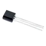
Figure 1. TO-92 Package
See NS Package LP0003A
Figure 2. Fully Protected Lamp Driver
1
2
Please be aware that an important notice concerning availability, standard warranty, and use in critical applications of
Texas Instruments semiconductor products and disclaimers thereto appears at the end of this data sheet.
All trademarks are the property of their respective owners.
PRODUCTION DATA information is current as of publication date.
Products conform to specifications per the terms of the Texas
Instruments standard warranty. Production processing does not
necessarily include testing of all parameters.
Copyright © 1998–2013, Texas Instruments Incorporated
�LP395
SNOSBF3C – APRIL 1998 – REVISED MARCH 2013
www.ti.com
These devices have limited built-in ESD protection. The leads should be shorted together or the device placed in conductive foam
during storage or handling to prevent electrostatic damage to the MOS gates.
ABSOLUTE MAXIMUM RATINGS (1)
Collector to Emitter Voltage
36V
Collector to Base Voltage
36V
Base to Emitter Voltage (Forward)
36V
Base to Emitter Voltage (Reverse)
10V
Base to Emitter Current (Reverse)
20 mA
Collector Current Limit
Internally Limited
Power Dissipation
Internally Limited
Operating Temperature Range
−40°C to +125°C
Storage Temperature Range
−65°C to +150°C
Lead Temp. (Soldering, 10 seconds)
(1)
260°C
Absolute Maximum Ratings indicate limits beyond which damage to the device may occur. Operating Ratings indicate conditions for
which the device is functional, but do not ensure specific performance limits.
ELECTRICAL CHARACTERISTICS
Symbol
VCE
Parameter
Collector to Emitter
Conditions
Typical
0.5 mA ≤ IC ≤ 100 mA
Tested Limit Design Limit
(1)
(2)
Units
(Limit)
36
36
V(Max)
(3)
Operating Voltage
ICL
Collector Current Limit
(4)
VBE = 2V, VCE = 36V
45
25
20
mA(Min)
VBE = 2V, VCE = 15V
90
60
50
mA(Min)
mA(Min)
VBE = 2V, 2V ≤ VCE ≤ 6V
130
100
100
IB
Base Current
0 ≤ IC ≤ 100 mA
−0.3
−2.0
−2.5
μA(Max)
IQ
Quiescent Current
VBE = 0V, 0 ≤ VCE ≤ 36V
0.24
0.50
0.60
mA(Max)
VCE(SAT)
Saturation Voltage
VBE = 2V, IC = 100 mA
1.82
2.00
2.10
V(Max)
BVBE
Base to Emitter Break-
0 ≤ VCE ≤ 36V, IB = 2 μA
36
36
V(Min)
0.79
0.90
V(Max)
1.40
V (Max)
down Voltage
VBE
(4)
Base to Emitter Voltage
(5)
tS
Switching Time
IC = 5 mA
IC = 100 mA
0.69
(4)
VCE = 20V, RL = 200Ω
1.02
μs
2
VBE = 0V, +2V, 0V
θJA
Thermal Resistance
0.4″ leads soldered to
Junction to Ambient
printed circuit board
0.125″ leads soldered to
printed circuit board
(1)
(2)
(3)
(4)
(5)
2
150
180
°C/W
(Max)
130
160
°C/W
(Max)
Specified and 100% production tested.
Specified (but not 100% production tested) over the operating temperature and supply voltage ranges. These limits are not used to
calculate outgoing quality levels.
Parameters identified with boldface type apply at temp. extremes. All other numbers, unless noted apply at +25°C.
These numbers apply for pulse testing with a low duty cycle.
Base positive with respect to emitter.
Submit Documentation Feedback
Copyright © 1998–2013, Texas Instruments Incorporated
Product Folder Links: LP395
�LP395
www.ti.com
SNOSBF3C – APRIL 1998 – REVISED MARCH 2013
SIMPLIFIED CIRCUIT
APPLICATIONS INFORMATION
One failure mode incandescent lamps may experience is one in which the filament resistance drops to a very low
value before it actually blows out. This is especially rough on most solid-state lamp drivers and in most cases a
lamp failure of this type will also cause the lamp driver to fail. Because of its high gain and blowout-proof design,
the LP395 is an ideal candidate for reliably driving small incandescent lamps. Additionally, the current limiting
characteristics of the LP395 are advantageous as it serves to limit the cold filament inrush current, thus
increasing lamp life.
Submit Documentation Feedback
Copyright © 1998–2013, Texas Instruments Incorporated
Product Folder Links: LP395
3
�LP395
SNOSBF3C – APRIL 1998 – REVISED MARCH 2013
www.ti.com
TYPICAL PERFORMANCE CHARACTERISTICS
4
5 Volt Transfer Function
36 Volt Transfer Function
Figure 3.
Figure 4.
Collector Characteristics
Available Collector Current
Figure 5.
Figure 6.
Quiescent Collector Current
Saturation Voltage
Figure 7.
Figure 8.
Submit Documentation Feedback
Copyright © 1998–2013, Texas Instruments Incorporated
Product Folder Links: LP395
�LP395
www.ti.com
SNOSBF3C – APRIL 1998 – REVISED MARCH 2013
TYPICAL PERFORMANCE CHARACTERISTICS (continued)
Collector Current Threshold
Figure 9.
Submit Documentation Feedback
Copyright © 1998–2013, Texas Instruments Incorporated
Product Folder Links: LP395
5
�LP395
SNOSBF3C – APRIL 1998 – REVISED MARCH 2013
www.ti.com
TYPICAL APPLICATIONS
Figure 10. Lamp Flasher
(Short Circuit Proof)
Figure 11. Optically Isolated
Switch
Figure 12. Two Terminal
Current Limiter
Figure 13. Composite PNP
6
Submit Documentation Feedback
Copyright © 1998–2013, Texas Instruments Incorporated
Product Folder Links: LP395
�LP395
www.ti.com
SNOSBF3C – APRIL 1998 – REVISED MARCH 2013
REVISION HISTORY
Changes from Revision B (March 2013) to Revision C
•
Page
Changed layout of National Data Sheet to TI format ............................................................................................................ 6
Submit Documentation Feedback
Copyright © 1998–2013, Texas Instruments Incorporated
Product Folder Links: LP395
7
�PACKAGE OPTION ADDENDUM
www.ti.com
10-Dec-2020
PACKAGING INFORMATION
Orderable Device
Status
(1)
Package Type Package Pins Package
Drawing
Qty
Eco Plan
(2)
Lead finish/
Ball material
MSL Peak Temp
Op Temp (°C)
Device Marking
(3)
(4/5)
(6)
LP395Z/LFT1
ACTIVE
TO-92
LP
3
2000
RoHS & Green
SN
N / A for Pkg Type
LP395Z/NOPB
ACTIVE
TO-92
LP
3
1800
RoHS & Green
SN
N / A for Pkg Type
LP
395Z
-40 to 125
LP
395Z
(1)
The marketing status values are defined as follows:
ACTIVE: Product device recommended for new designs.
LIFEBUY: TI has announced that the device will be discontinued, and a lifetime-buy period is in effect.
NRND: Not recommended for new designs. Device is in production to support existing customers, but TI does not recommend using this part in a new design.
PREVIEW: Device has been announced but is not in production. Samples may or may not be available.
OBSOLETE: TI has discontinued the production of the device.
(2)
RoHS: TI defines "RoHS" to mean semiconductor products that are compliant with the current EU RoHS requirements for all 10 RoHS substances, including the requirement that RoHS substance
do not exceed 0.1% by weight in homogeneous materials. Where designed to be soldered at high temperatures, "RoHS" products are suitable for use in specified lead-free processes. TI may
reference these types of products as "Pb-Free".
RoHS Exempt: TI defines "RoHS Exempt" to mean products that contain lead but are compliant with EU RoHS pursuant to a specific EU RoHS exemption.
Green: TI defines "Green" to mean the content of Chlorine (Cl) and Bromine (Br) based flame retardants meet JS709B low halogen requirements of
很抱歉,暂时无法提供与“LP395Z/NOPB”相匹配的价格&库存,您可以联系我们找货
免费人工找货- 国内价格 香港价格
- 1+26.716451+3.46296
- 10+17.2708110+2.23863
- 100+11.89927100+1.54238
- 500+9.60368500+1.24482
- 1800+8.333181800+1.08014
- 3600+7.797943600+1.01077
- 5400+7.548885400+0.97848
- 国内价格
- 1+10.43280
- 10+10.18440
- 30+10.02240