User's Guide
SNVA235A – May 2007 – Revised April 2013
AN-1621 LP3972 USB Evaluation Board Rev B
1
General Description
The LP3972 Flex PMU is a complete power management IC designed for advanced processors. It
contains 5 low noise low dropout regulators, 3 DC/DC buck converters, a backup battery charger, real
time clock supply regulator [RTC], 2 GPO’s and high speed I2C serial interface to program individual
regulator output voltages as well as offer on/off control. This USB evaluation board features independent
USB powering, virtual voltmeter bank all in a compact demonstration platform.
2
Key Features
•
•
•
•
•
3
Applications
•
•
•
•
4
2.7V to 5.5V input voltage range
Programmable VOUT 0.8 to 3.3 volts
Up to 95% efficiency
±3% output voltage accuracy
1.5A output current [bucks]
Personal Media Players
Smart Phones
PDA Phones
Digital Cameras
Evaluation Board/Kit Overview
The LP3972 Evaluation Board supports complete functional evaluation of the power management IC. The
functions of the chip are controlled by the I2C interface. The I2C interface on the rev B and later USB
boards are driven via a COP8 microprocessor which supports a connection via the USB port and offers
chip powering and virtual software voltage measurement of all regulators. In addition, the LP3972 can be
powered directly through the USB port for full function. If high current Buck testing is desired, an external
LI ION cell or PS capable of supplying 2 amps or more will need to be connected to the appropriate
connector.
The evaluation board/kit consists of:
• LP3972 Flex_PMU device soldered down in RSB-40 pin 5X5 WQFN package
• Full USB interface
• LED LDO monitoring with current limit resistors [selectable]
• External power LDO, Buck output and main battery/supply connectors offered in heavy duty turret pins
and solder pads
• Socket for back-up battery
• Users guide
• Codeloader Software version 1.2.0.2 or greater [may be sent via email]
All trademarks are the property of their respective owners.
SNVA235A – May 2007 – Revised April 2013
Submit Documentation Feedback
AN-1621 LP3972 USB Evaluation Board Rev B
Copyright © 2007–2013, Texas Instruments Incorporated
1
�Evaluation Board/Kit Overview
www.ti.com
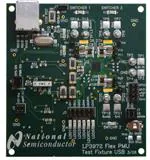
Figure 1. LP3972 Evaluation Board Version B
USB B connector
Power selection
USB/External
External VCC Pads
/Turret pins
USB 9604
Full speed node controller
Enhanced DMA support
SDA/SCL
communications
COP8CBDE9
8 Bit CMOS microcontroller with
8K memory, 10 Bit AD converter
LP3972
FlexPMU
Buck switcher ouputs
and LED monitoring
Analog to Digital conversion
voltmeter lines
LDO outputs and LED
monitoring
Figure 2. LP3972 Flex_PMU USB Evaluation Board Block Operational Diagram
2
AN-1621 LP3972 USB Evaluation Board Rev B
Copyright © 2007–2013, Texas Instruments Incorporated
SNVA235A – May 2007 – Revised April 2013
Submit Documentation Feedback
�Pin Description 5 × 5 Package
www.ti.com
5
Pin Description 5 × 5 Package
Pin #
(1)
I/O
1
PKEY
I
D
CPU Wakeup Input
2
nTJ
I
D
CPU Wakeup Input
3
SP
I
D
CPU Wakeup Input
4
EXT_WAKEUP
O
D
CPU Wakeup Input
5
FB1, Feedback Buck1
I
A
Buck 1 Feedback
6
VIN1 = VBATT
I
P
Battery Input for Powering Internal
Circuits and LDO1-3
7
LDO_VOUT_1
O
P
LDO1 Output
8
LDO_VOUT_2
O
P
LDO2 Output
9
nRST In
I
D
Chip Reset Input
10
LDO GND 1
G
G
Ground
11
LDO VREF Bypass
O
A
Bypass Capacitor for Reference
12
LDO_VOUT_3
O
P
LDO3 Output
13
LDO_VOUT_4
O
P
LDO4 Output
14
VIN LDO_4
I
P
Input Power for LDO4
15
Back-Up Battery VIN
I
P
Back Up Battery Input
16
LDO_VOUT_0 (RTC)
O
P
LDO_RTC Output
17
nBatt_FLT
O
D
Main Battery Fault Output
18
PGND Buck2
G
G
Ground
19
VOUT Buck2
O
P
Buck Switcher2 Output
20
VIN Buck2
I
P
Buck Switcher 2 Battery Input
21
SDA
I/O
D
I2C Data Line
22
SCL
I
D
I2C Clock Input
23
FB2, Feedback Buck2
I
A
Buck Switcher 2 Feedback
24
nRST Out
O
D
Reset Output
25
LDO_VOUT_5
O
P
LDO5 Output
26
VIN2 (LDO 5 Only)
I
P
Battery Input Power for LDO5
27
VDDA
I
P
Analog Power Input
28
FB3, Feedback Buck3
I
A
Buck Switcher 3 Feedback
29
GPIO1/nCHG_EN
I/O
D
General Purpose I/O #1/BUBATT
Charger EN
30
GPIO2
I/O
D
General Purpose I/O #2
31
VIN Buck3
I
P
Buck Switcher 3 Battery Input
32
VOUT Buck3
I
P
Buck Switcher 2 Output
33
PGND Buck3
G
G
Buck3 NMOS Power Ground
34
Buck 1 2 & 3 AVSS/NCHBLK
G
G
Buck1, 2, 3 Analog Ground
35
SYNC (Buck Clock input)
I
D
Buck Switcher External Clock Input
36
Sys_En
I
D
Power Domain Enable
37
Pwr_En
I
D
Power Domain Enable
38
PGND Buck1
G
G
Buck1 NMOS Power Ground
39
VOUT Buck1
O
P
Buck Switcher 1 Output
VIN Buck1
I
P
Buck Switcher 1 Battery Input
40
(1)
Type
(1)
Name
Description
A: Analog Pin; D: Digital Pin; G: Ground Pin; I: Input Pin; I/O: Input/Output; O: Output Pin; P: Power Pin
SNVA235A – May 2007 – Revised April 2013
Submit Documentation Feedback
AN-1621 LP3972 USB Evaluation Board Rev B
Copyright © 2007–2013, Texas Instruments Incorporated
3
�Operating Instructions
6
www.ti.com
Operating Instructions
The following instructions give general instructions for use of LP3972 with the evaluation board. Practice
standard ESD protection (ground cable) to prevent any unwanted damaging ESD events.
1. Check that the jumpers are in default settings (jumpers are introduced later in this document).
2. Load version .202 or later of the codeloader program into PC.
3. Connect the USB cable [standard USB AB cable] from the USB connector to PC port.
4. Open the codeloader program up, verify that “USB” port has been selected.
5. Verify that successful communications link has been established by toggling “READ ALL”.
6. If there is no communication, key the USB RST [SW1] switch once on the board for reboot.
7. If the voltmeter monitoring function is desired, select “POLL STATUS”.
8. LDO/buck outputs may be monitored directly off the appropriate header output pins.
9. Note that for full load testing, an external PS must be connected to TP1/TP2 and jumper J1 must be
removed. This is because the USB port source spec is limited to 500 mA and removing the jumper will
disconnect the USB supply.
10. PWR EN/SYS En is selectable via codeloader software assignment.
11. Hardware reset can be accomplished by pressing the nREST_In momentary switch.
12. Battery backup is possible by inserting appropriate rechargeable cell into supplied holder.
13. Switches PKEY, nTJ, and SP, are provided for use in normal evaluation mode.
7
4
List of Components
Item
Qty
Reference
Value
Pkg.
Manuf.
Part Number
1
5
C1,C21,CC,CD,CF1
10 µF
0805
Panasonic
ECJ2FF1A106Z
2
2
C2,C3
100 µF
3528-21
Kemet
T520B107M006ASE040
3
8
C4,C7,C13,C15,C16,C31,CA
,CB
1 µF
0805
Kemet
C0805C105K4RACTU
4
6
C5,C6,C8,C9,C25,C29
10 µf
1206
Taiyo-Yuden
JMK316BJ106M
5
6
C14,C19,C20,C23,C24,C26
0.47 µF
0805
TDK
C2012X7R1E474K
6
2
C17,C18
47 pF
0805
Murata
GRM2195C2A470JZ01D
7
4
C22,C30,C32,C33
0.1 µF
0805
Murata
GRM21BR71E104KA01L
8
2
C27,C28
15 pF
0805
Yageo
0805CG150J9B200
9
1
BT2
Battery Holder
SMT
Seiko
BH0414
10
1
NOT INSTALLED
Backup Battery
Micro4
Seiko
MS412F
11
4
D6,D7,D10,D11
Schottky
PM 457
On Semi
MBRM120LT3
12
2
D8 (PWR EN), D9 (SYS EN)
Green LED
1206
Lumex
SML-LX1206GC-TR
13
9
LDO1(D13), LDO2(D14),
LDO3(D18), LDO4(D17),
LDO5(D19), LDORTC(D16)
D2,D3,D12
Red LED
1206
Lumex
SML-LX1206IC-TR
14
2
L1,L2
1 µH Inductor
0805
TDK
MLF2012A1R0K
15
3
L3,L4,L5
2.2 µH Inductor
SMT
Toko
FDSE0312
16
1
Q1
XTAL 24 MHz 18 PF
SMD
Citizen
HCM49-24.000MABJT
17
7
R1,R2,R23,R31,R32,R33,R3
4
330Ω
0805
SEI
807065R330
18
1
R8
100Ω
0805
NIC
NRC10J101TR
19
1
R9
49.9Ω
0805
Rohm
MCR10EZHF49R9
20
11
R10,R11,R12,R17,R18,R22,
R24,R26,R27,R36,R37
10K
0805
Yageo
9C08052A1002FKHFT
21
1
R12
0Ω
0805
Yaego
9C08052A0R00JLHFT
AN-1621 LP3972 USB Evaluation Board Rev B
Copyright © 2007–2013, Texas Instruments Incorporated
SNVA235A – May 2007 – Revised April 2013
Submit Documentation Feedback
�List of Components
www.ti.com
Item
Qty
Reference
Value
Pkg.
22
4
23
2
24
1
25
1
26
1
27
5
28
1
29
R15,R16,R28,R29
133Ω
0805
Rohm
MCR10EZHF1330
R19,R20
22.1Ω
0805
Vishay-Dale
CRCW080522R1ERT1
R21
1M
0805
Yageo
9C08052A1004JLHFT
R25
1.5K
0805
Yageo
9C08052A1501FKHFT
D1
45.3Ω
0805
Vishay-Dale
CRCW080545R3F100
S1,S2,S3,S4,SW1
Touch Switch
SMD
Panasonic
EVQ-PJU04K
U1
3.3V Regulator
SOT-23 5
Texas
Instruments
LP29815-3.3
1
U2
PMU
RSB0040
Texas
Instruments
LP3972
30
1
U3
USB Controller
SOIC 28
Texas
Instruments
USBN9604-28M
31
1
U4
Microcontroller
TSSOP 48
Texas
Instruments
COP8CBE9
32
1
U5
2V Regulator
SOT-23 5L
Texas
Instruments
LP3984-2.0
33
1
U6
Voltage Converter
SOT-23-6
Texas
Instruments
LM2664M6
34
1
J1
100 mil Header
2 pos
Amp
1 × 2 (4-103239-0-02)
35
1
J2
USB Receptacle
4 pos
FCI
61729-0010B
36
1
J3
100 mil Header
4 pos
Molex
1 × 4 (22-10-2041)
37
3
J4,J7,J8
100 mil Header
4 pos
Amp
2 × 2 (4-103240-0-02)
38
1
J5
100 mil Header
12 pos
Amp
2 × 6 (4-103240-0-06)
39
1
J6
GPO/LDO Headers
8 pos
Amp
2 × 4 (4-103186-0-04)
40
9
TP9,TP10,TP11,TP16,
TP17,TP18,TP23,TP24,TP25
Test Points
1 pos
Amp
1 × 1 (4-103185-0-01)
41
8
TP2,TP4,TP6,TP8,TP13,
TP15,TP20,TP22
Turret Terminal
0.109"L
Keystone
1502-2
42
1
LP3972 version B Fab
Bare board
4 Layer
Rainbow Labs
LP3972-B
SNVA235A – May 2007 – Revised April 2013
Submit Documentation Feedback
Manuf.
Part Number
AN-1621 LP3972 USB Evaluation Board Rev B
Copyright © 2007–2013, Texas Instruments Incorporated
5
�Powering and Jumpers Selection
8
www.ti.com
Powering and Jumpers Selection
The LP3972 USB evaluation platform offers several power connectors. These connectors are outlined on
the table below. In addition, the Evaluation board has jumpers for special modes and stand-alone use.
The default jumper settings are valid in normal operation and are also outlined below.
Component
6
Use
Comment
J5-1
Output for LDO1
Outside Pin of Connector is Grd
J5-2
Output for LDO2
Outside Pin of Connector is Grd
J5-3
Output for LDO3
Outside Pin of Connector is Grd
J5-4
Output for LDO4
Outside Pin of Connector is Grd
J5-6
Output for LDO5
Use LED Pad [Missed Pin]
J5-5
Output for RTC [Real time Clock]
Outside Pin of Connector is Grd
J4-1
Input for external wakeup
Outside Pin of Connector is Grd
J4-2
Output for nBATT Fault
Outside Pin of Connector is Grd
J6-2
Output for nREST
Outside Pin of Connector is Grd
J6-3
GPO 1 output
Outside Pin of Connector is Grd
J6-4
GPO 2 output
Outside Pin of Connector is Grd
J3-1
Cop8 microwire SO
Used for Micro Flash Only
J3-2
Cop8 microwire SK
Used for Micro Flash Only
J3-3
Cop8 microwire SI
Used for Micro Flash Only
J3-4
Cop 8 Grd
Used for Micro Flash Only
TP14-15
Output for Buck switcher 1
GRD is TP12-13
TP19-20
Output for Buck switcher 2
GRD is TP21-22
TP5-6
Output for Buck switcher 3
GRD is 7-8
USB
USB connector
Connect to PC via Supplied Cable
J1
Power usage selection
Place Jumper for USB, NO JUMPER for
External Power Input
TP1-2
Connect external VCC supply here 3.5-5 volts
for high current testing
Doubles for LI-ION Cell Input, Select
Appropriate J1 Setting [2-3]
AN-1621 LP3972 USB Evaluation Board Rev B
Copyright © 2007–2013, Texas Instruments Incorporated
SNVA235A – May 2007 – Revised April 2013
Submit Documentation Feedback
�Demonstration Software Window
www.ti.com
9
Demonstration Software Window
The demonstration software enables read and write to LP3972’s internal registers through PC’s USB port.
All the user controllable registers are usable through the software.
Installation: Run the codeloader for LP3972 version .202 or greater.
After startup the user can verify that successful USB communication has been established by selecting
“Read All”, the default programmed voltages should appear.
LDO’s can be enabled and disabled by clicking mouse left button on the square close to each LDO
voltage slider. Changing the virtual slider changes the LDO voltage. After the WRITE button is pressed
subsequent LDO changes are applied if the ‘autowrite’ feature is disabled.
Note ‘Autowrite’ enabled is default. In the case of the buck control, an option for ‘hold’ or ‘go’ can be
selected. Note voltage will not change until the ‘go’ selection is made.
The virtual voltmeters can be activated by selecting ‘Poll Status’, after which an A to D conversion is read
and displayed for each subsequent LDO and Buck output. Note that this feature is meant to be a general
measurement and “may” be subject to variations due to operations noise. Since there is a bi-directional
SDA feature, any register and its contents can be determined by entering the desired register address and
selecting ‘Read’. In addition, any corresponding register may be written directly to via the ‘Store’ selection.
All virtual sliders can be updated via the ‘Read All’ Tab. Direct register control is possible by entering the
desired address and value followed by a ‘Store’ command.
Figure 3. Control Panel
SNVA235A – May 2007 – Revised April 2013
Submit Documentation Feedback
AN-1621 LP3972 USB Evaluation Board Rev B
Copyright © 2007–2013, Texas Instruments Incorporated
7
�Layout Details
10
www.ti.com
Layout Details
Figure 4. Top Silkscreen
Figure 5. Top Trace
8
AN-1621 LP3972 USB Evaluation Board Rev B
Copyright © 2007–2013, Texas Instruments Incorporated
SNVA235A – May 2007 – Revised April 2013
Submit Documentation Feedback
�Layout Details
www.ti.com
Figure 6. Bottom Trace
Figure 7. Bottom Silkscreen
SNVA235A – May 2007 – Revised April 2013
Submit Documentation Feedback
AN-1621 LP3972 USB Evaluation Board Rev B
Copyright © 2007–2013, Texas Instruments Incorporated
9
�Layout Details
www.ti.com
Figure 8. Ground Plane
Figure 9. Power Plane
10
AN-1621 LP3972 USB Evaluation Board Rev B
Copyright © 2007–2013, Texas Instruments Incorporated
SNVA235A – May 2007 – Revised April 2013
Submit Documentation Feedback
�Layout Details
www.ti.com
Figure 10. Bare Board/Component Locations
SNVA235A – May 2007 – Revised April 2013
Submit Documentation Feedback
AN-1621 LP3972 USB Evaluation Board Rev B
Copyright © 2007–2013, Texas Instruments Incorporated
11
�LP3972 Flex_PMU Evaluation Board Schematic
11
www.ti.com
LP3972 Flex_PMU Evaluation Board Schematic
Figure 11. LP3972 Flex_PMU Evaluation Board Schematic
12
AN-1621 LP3972 USB Evaluation Board Rev B
SNVA235A – May 2007 – Revised April 2013
Submit Documentation Feedback
Copyright © 2007–2013, Texas Instruments Incorporated
�IMPORTANT NOTICE
Texas Instruments Incorporated and its subsidiaries (TI) reserve the right to make corrections, enhancements, improvements and other
changes to its semiconductor products and services per JESD46, latest issue, and to discontinue any product or service per JESD48, latest
issue. Buyers should obtain the latest relevant information before placing orders and should verify that such information is current and
complete. All semiconductor products (also referred to herein as “components”) are sold subject to TI’s terms and conditions of sale
supplied at the time of order acknowledgment.
TI warrants performance of its components to the specifications applicable at the time of sale, in accordance with the warranty in TI’s terms
and conditions of sale of semiconductor products. Testing and other quality control techniques are used to the extent TI deems necessary
to support this warranty. Except where mandated by applicable law, testing of all parameters of each component is not necessarily
performed.
TI assumes no liability for applications assistance or the design of Buyers’ products. Buyers are responsible for their products and
applications using TI components. To minimize the risks associated with Buyers’ products and applications, Buyers should provide
adequate design and operating safeguards.
TI does not warrant or represent that any license, either express or implied, is granted under any patent right, copyright, mask work right, or
other intellectual property right relating to any combination, machine, or process in which TI components or services are used. Information
published by TI regarding third-party products or services does not constitute a license to use such products or services or a warranty or
endorsement thereof. Use of such information may require a license from a third party under the patents or other intellectual property of the
third party, or a license from TI under the patents or other intellectual property of TI.
Reproduction of significant portions of TI information in TI data books or data sheets is permissible only if reproduction is without alteration
and is accompanied by all associated warranties, conditions, limitations, and notices. TI is not responsible or liable for such altered
documentation. Information of third parties may be subject to additional restrictions.
Resale of TI components or services with statements different from or beyond the parameters stated by TI for that component or service
voids all express and any implied warranties for the associated TI component or service and is an unfair and deceptive business practice.
TI is not responsible or liable for any such statements.
Buyer acknowledges and agrees that it is solely responsible for compliance with all legal, regulatory and safety-related requirements
concerning its products, and any use of TI components in its applications, notwithstanding any applications-related information or support
that may be provided by TI. Buyer represents and agrees that it has all the necessary expertise to create and implement safeguards which
anticipate dangerous consequences of failures, monitor failures and their consequences, lessen the likelihood of failures that might cause
harm and take appropriate remedial actions. Buyer will fully indemnify TI and its representatives against any damages arising out of the use
of any TI components in safety-critical applications.
In some cases, TI components may be promoted specifically to facilitate safety-related applications. With such components, TI’s goal is to
help enable customers to design and create their own end-product solutions that meet applicable functional safety standards and
requirements. Nonetheless, such components are subject to these terms.
No TI components are authorized for use in FDA Class III (or similar life-critical medical equipment) unless authorized officers of the parties
have executed a special agreement specifically governing such use.
Only those TI components which TI has specifically designated as military grade or “enhanced plastic” are designed and intended for use in
military/aerospace applications or environments. Buyer acknowledges and agrees that any military or aerospace use of TI components
which have not been so designated is solely at the Buyer's risk, and that Buyer is solely responsible for compliance with all legal and
regulatory requirements in connection with such use.
TI has specifically designated certain components as meeting ISO/TS16949 requirements, mainly for automotive use. In any case of use of
non-designated products, TI will not be responsible for any failure to meet ISO/TS16949.
Products
Applications
Audio
www.ti.com/audio
Automotive and Transportation
www.ti.com/automotive
Amplifiers
amplifier.ti.com
Communications and Telecom
www.ti.com/communications
Data Converters
dataconverter.ti.com
Computers and Peripherals
www.ti.com/computers
DLP® Products
www.dlp.com
Consumer Electronics
www.ti.com/consumer-apps
DSP
dsp.ti.com
Energy and Lighting
www.ti.com/energy
Clocks and Timers
www.ti.com/clocks
Industrial
www.ti.com/industrial
Interface
interface.ti.com
Medical
www.ti.com/medical
Logic
logic.ti.com
Security
www.ti.com/security
Power Mgmt
power.ti.com
Space, Avionics and Defense
www.ti.com/space-avionics-defense
Microcontrollers
microcontroller.ti.com
Video and Imaging
www.ti.com/video
RFID
www.ti-rfid.com
OMAP Applications Processors
www.ti.com/omap
TI E2E Community
e2e.ti.com
Wireless Connectivity
www.ti.com/wirelessconnectivity
Mailing Address: Texas Instruments, Post Office Box 655303, Dallas, Texas 75265
Copyright © 2013, Texas Instruments Incorporated
�


 工商网监
湘ICP备2023018690号
工商网监
湘ICP备2023018690号