Sample &
Buy
Product
Folder
Support &
Community
Tools &
Software
Technical
Documents
LP8728C-Q1
SNVSA71 – FEBRUARY 2015
LP8728C-Q1 Quad-Output Step-Down DC-DC Converter
1 Features
3 Description
•
The LP8728C-Q1 is a quad-output Power
Management Unit (PMU), optimized for low-power
FPGAs, microprocessors, and DSPs for automotive
applications. This device integrates four highly
efficient step-down DC-DC converters into one
package. Each converter has high current capability
and separate controls which allows flexibility to use
the device in multiple applications. All the converters
operate above the AM band with a fixed 3.2-MHz
switching frequency. The high-side switch turn-on
time of each converter is phase shifted to minimize
input current spikes.
1
•
•
•
•
•
•
LP8728C-Q1 is an Automotive Grade Product that
is AECQ-100 Grade 1 Qualified
Four High Efficiency Step-Down DC-DC
Converters:
– 93% Peak Efficiency (VIN = 5 V, VOUT = 3.3 V)
– Max Output Current 1 A
– Forced PWM Operation
– Soft-Start Control
– VOUT1 = 3.3 V
– VOUT2 = 1.2 V
– VOUT3 = 1.8 V or 2.65 V (pin selectable)
– VOUT4 = 1.8 V
Separate Enable Inputs for each Converter
Control
Separate Power Good Outputs for each Converter
Output Overcurrent and Input Overvoltage
Protection
Overtemperature Protection
Undervoltage Lockout (UVLO)
2 Applications
•
•
•
•
•
Protection features include output short-circuit
protection, switch current limits, input overvoltage
protection, input undervoltage lockout, and thermal
shutdown functions. During start-up, the device
controls the output slew rate to minimize output
voltage overshoot and the input inrush current.
Device Information(1)
PART NUMBER
LP8728C-Q1
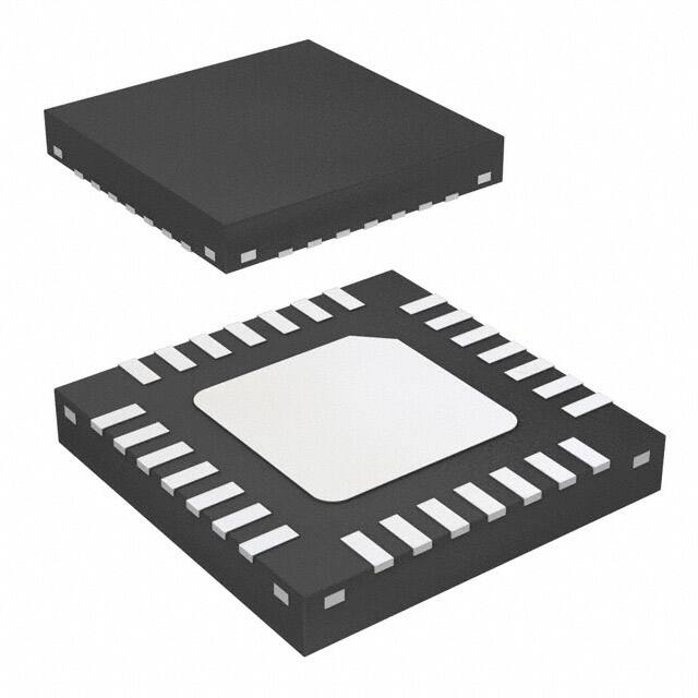
PACKAGE
WQFN (28)
BODY SIZE (NOM)
5.00 mm x 5.00 mm
(1) For all available packages, see the orderable addendum at
the end of the datasheet.
space
FPGA, DSP Core Power
Processor Power for Mobile Devices
Peripheral I/O Power
Automotive Safety Cameras
Automotive Infotainment
space
space
space
space
space
Simplified Schematic
VIN
Efficiency
VIN
10 µF
VIN_B1
AVDD
1 µF
100
1.5 µH
FB_B1
1 µF
1.5 µH
VOUT2
10 µF
SW_B2
FB_B2
LP8728
PG_B1
VIN
10 µF
VIN_B3
PG_B2
PG_B3
1.5 µH
PG_B4
SW_B3
EN_B1
FB_B3
VOUT3
10 µF
VIN_B4
VIN
EN_B2
EN_B3
10 µF
GND_B3
GND_B4
GND_B2
AGND
DEFSEL
GND_B1
EN_B4
1.5 µH
SW_B4
FB_B4
EFFICIENCY (%)
80
VIN
10 µF
VIN_B2
VDDIO
Micro
Controller
90
VOUT1
10 µF
SW_B1
BYP
70
60
50
40
30
3.3V
2.65V
1.8V
1.2V
20
10
VOUT4
10 µF
0
0.0
0.1
0.2
0.3
0.4
0.5 0.6
IOUT (A)
0.7
0.8
0.9
1.0
D019
1
An IMPORTANT NOTICE at the end of this data sheet addresses availability, warranty, changes, use in safety-critical applications,
intellectual property matters and other important disclaimers. PRODUCTION DATA.
�LP8728C-Q1
SNVSA71 – FEBRUARY 2015
www.ti.com
Table of Contents
1
2
3
4
5
6
7
Features ..................................................................
Applications ...........................................................
Description .............................................................
Revision History.....................................................
Pin Configuration and Functions .........................
Specifications.........................................................
1
1
1
2
3
5
6.1
6.2
6.3
6.4
6.5
6.6
6.7
5
5
5
6
6
7
8
Absolute Maximum Ratings ......................................
ESD Ratings..............................................................
Recommended Operating Conditions.......................
Thermal Information ..................................................
Electrical Characteristics...........................................
System Characteristics .............................................
Typical Characteristics ..............................................
7.3 Feature Description................................................. 11
7.4 Device Functional Modes........................................ 13
8
Application and Implementation ........................ 15
8.1 Application Information............................................ 15
8.2 Typical Application ................................................. 15
9 Power Supply Recommendations...................... 17
10 Layout................................................................... 18
10.1 Layout Guidelines ................................................. 18
10.2 Layout Example .................................................... 18
11 Device and Documentation Support ................. 19
11.1
11.2
11.3
11.4
11.5
Detailed Description ............................................ 10
7.1 Overview ................................................................. 10
7.2 Functional Block Diagram ....................................... 10
Device Support ....................................................
Related Documentation.........................................
Trademarks ...........................................................
Electrostatic Discharge Caution ............................
Glossary ................................................................
19
19
19
19
19
12 Mechanical, Packaging, and Orderable
Information ........................................................... 19
4 Revision History
2
DATE
REVISION
NOTES
February 2015
*
Initial release.
Submit Documentation Feedback
Copyright © 2015, Texas Instruments Incorporated
Product Folder Links: LP8728C-Q1
�LP8728C-Q1
www.ti.com
SNVSA71 – FEBRUARY 2015
5 Pin Configuration and Functions
WQFN (RSG) Package
28 Pins
VIN_B2
SW_B2
GND_B2
GND_B1
SW_B1
VIN_B1
EN_B1
TOP VIEW
7
6
5
4
3
2
1
PIN 1 ID
FB_B2
8
28
FB_B1
EN_B2
9
27
PG_B1
PG_B2
10
26
AVDD
DEFSEL
11
25
BYP
PG_B3
12
24
AGND
EN_B3
13
23
PG_B4
FB_B3
14
22
FB_B4
18
19
20
21
SW_B4
VIN_B4
EN_B4
SW_B3
17
GND_B4
16
GND_B3
15
VIN_B3
DAP
Pin Functions
PIN
NUMBER
(1)
NAME
TYPE (1)
DESCRIPTION
1
EN_B1
D/I
2
VIN_B1
P
Enable Buck 1
Positive power supply input for Buck 1
3
SW_B1
P
Switch node for Buck 1
4
GND_B1
G
Power ground for Buck 1
5
GND_B2
G
Power ground for Buck 2
6
SW_B2
P
Switch node for Buck 2
7
VIN_B2
P
Positive power supply input for Buck 2
Feedback pin for Buck 2. Referenced against AGND.
8
FB_B2
A
9
EN_B2
D/I
Enable Buck 2
10
PG_B2
D/O
Open-drain Power Good output for Buck 2
11
DEFSEL
D/I
Buck 3 output voltage selection pin
12
PG_B3
D/O
Open-drain Power Good output for Buck 3
13
EN_B3
D/I
Enable Buck 3
14
FB_B3
A
Feedback pin for Buck 3. Referenced against AGND.
15
VIN_B3
P
Positive power supply input for Buck 3
16
SW_B3
P
Switch node for Buck 3
17
GND_B3
G
Power ground for Buck 3
18
GND_B4
G
Power ground for Buck 4
19
SW_B4
P
Switch node for Buck 4
A: Analog Pin, G: Ground Pin, P: Power Pin, O: Output Pin, D/I: Digital Input, D/O: Digital Output.
Submit Documentation Feedback
Copyright © 2015, Texas Instruments Incorporated
Product Folder Links: LP8728C-Q1
3
�LP8728C-Q1
SNVSA71 – FEBRUARY 2015
www.ti.com
Pin Functions (continued)
PIN
4
TYPE (1)
DESCRIPTION
NUMBER
NAME
20
VIN_B4
P
21
EN_B4
D/I
22
FB_B4
A
23
PG_B4
D/O
24
AGND
G
Analog ground
25
BYP
A
Internal 1.8-V supply voltage capacitor pin. A ceramic low-ESR 1-μF capacitor should
be connected from this pin to AGND. The BYP voltage is generated internally, do not
supply or load this pin externally.
Positive power supply input for Buck 4
Enable Buck 4
Feedback pin for Buck 4. Referenced against AGND.
Open-drain Power Good output for Buck 4
26
AVDD
P
Analog positive power supply pin (VIN level)
27
PG_B1
D/O
Open-drain Power Good output for Buck 1
28
FB_B1
A
DAP
Die Attachment Pad
Feedback pin for Buck 1. Referenced against AGND.
Exposed die attachment pad should to be connected to GND plane with thermal vias
to improve the thermal performance of the system.
Submit Documentation Feedback
Copyright © 2015, Texas Instruments Incorporated
Product Folder Links: LP8728C-Q1
�LP8728C-Q1
www.ti.com
SNVSA71 – FEBRUARY 2015
6 Specifications
6.1 Absolute Maximum Ratings
over operating free-air temperature range (unless otherwise noted) (1)
VIN
Voltage on power pins (AVDD, VIN_Bx)
VFB
Voltage on feedback pins (FB_Bx)
VSW
Voltage on buck converter switch pins (SW_Bx)
VDIG
Voltage on digital pins (PG_Bx, EN_Bx, DEFSEL)
VBYP
Voltage on BYP pin
TJ(MAX)
Maximum operating junction temperature (2)
MIN
MAX
UNIT
–0.3
6
V
–0.3
6
V
(GND_Bx – 0.2 V) to (VIN_Bx + 0.2 V) with 6 V max
V
(AGND – 0.2V) to (AVDD + 0.2 V) with 6 V max
V
–0.3
(1)
(2)
(3)
V
°C
150
°C
See (3)
Maximum lead temperature (Soldering)
Tstg
2
150
Storage temperature
–65
Stresses beyond those listed under Absolute Maximum Ratings may cause permanent damage to the device. These are stress ratings
only, which do not imply functional operation of the device at these or any other conditions beyond those indicated under Recommended
Operating Conditions. Exposure to absolute-maximum-rated conditions for extended periods may affect device reliability.
Internal thermal shutdown circuitry protects the device from permanent damage. Thermal shutdown engages at TJ = 150°C (typical) and
disengages at TJ = 130°C (typical).
For detailed soldering specifications and information, please refer to Texas Instruments Application Note Leadless Leadframe Package
(LLP) SNOA401.
6.2 ESD Ratings
VALUE
V(ESD)
(1)
Electrostatic discharge
Human-body model (HBM), per AEC Q100-002
(1)
UNIT
±2000
Charged-device model (CDM), per AEC Q100-011
V
±750
AEC Q100-002 indicates that HBM stressing shall be in accordance with the ANSI/ESDA/JEDEC JS-001 specification.
6.3 Recommended Operating Conditions
over operating free-air temperature range (unless otherwise noted) (1)
MIN
NOM
MAX
VIN
Input voltage on AVDD, VIN_B1, VIN_B2, VIN_B3 and VIN_B4 pins
4.5
5
5.5
V
TA
Operating ambient temperature (2)
–40
125
°C
COUT
Effective output capacitance during operation.
Min value over TA –40°C to 125°C.
12
µF
CIN
Effective input capacitance during operation. 4.5 V ≤ VIN_Bx ≤ 5.5 V.
Min value over TA –40°C to 125°C.
L
Effective inductance during operation
Min value over TA –40°C to 125°C.
(1)
(2)
5
10
2.5
10
0.47
1.5
UNIT
µF
2
µF
All voltage values are with respect to network ground terminal.
In applications where high power dissipation and/or poor package thermal resistance is present, the maximum ambient temperature may
have to be derated. Maximum ambient temperature (TA(max)) is dependent on the maximum operating junction temperature (TJ(max)), the
maximum power dissipation of the device in the application (PD(max)), and the junction-to-ambient thermal resistance of the part/package
in the application (RθJA), as given by the following equation: TA(max) = TJ(max) – (RθJA × PD(max))
Submit Documentation Feedback
Copyright © 2015, Texas Instruments Incorporated
Product Folder Links: LP8728C-Q1
5
�LP8728C-Q1
SNVSA71 – FEBRUARY 2015
www.ti.com
6.4 Thermal Information
LP8728-Q1
THERMAL METRIC (1)
WQFN (RSG)
UNIT
28 PINS
RθJA
Junction-to-ambient thermal resistance (2)
37.7
RθJCtop
Junction-to-case (top) thermal resistance
24.5
RθJB
Junction-to-board thermal resistance
10.8
ΨJT
Junction-to-top characterization parameter
0.3
ΨJB
Junction-to-board characterization parameter
10.8
RθJCbot
Junction-to-case (bottom) thermal resistance
2.7
(1)
(2)
°C/W
For more information about traditional and new thermal metrics, see the IC Package Thermal Metrics application report, SPRA953.
Calculated using 4-layer standard JEDEC thermal test board with 5 thermal vias between the die attach pad in the first copper layer and
second copper layer.
6.5 Electrical Characteristics (1) (2)
Unless otherwise noted, VIN = 5 V, typical values apply for TA = 25°C, and minimum/maximum limits apply over junction
temperature range, TJ = –40°C to 125°C.
PARAMETER
TEST CONDITIONS
ISHDN
Shutdown supply current into power
connections
EN_Bx = 0 V
IOP
Operating current
All buck-converters active, IOUT = 0 mA
MIN
TYP
MAX
1
6
20
UNIT
μA
mA
LOGIC INPUTS (EN_Bx, DEFSEL)
VIL
Input low level
0.4
V
VIH
Input high level
1.6
RPD_DI
EN_Bx and DEFSEL internal
pulldown resistance
300
TH_MIN
Minimum EN_Bx high time
1
ms
TL_MIN
Minimum EN_Bx low time
10
µs
V
520
820
kΩ
LOGIC OUTPUTS (PG_Bx)
VOL
Output low level
RPU
Recommended pullup resistor
ISINK = 3 mA
0.4
V
10
kΩ
3.3
V
V
BUCK CONVERTERS
VOUT1
Output voltage for Buck 1
Fixed voltage
VOUT2
Output voltage for Buck 2
Fixed voltage
1.2
DEFSEL = 1
2.65
DEFSEL = 0
1.8
VOUT3
Output voltage for Buck 3
VOUT4
Output voltage for Buck 4
VFB_Bx
Output voltage accuracy
Fixed voltage
V
1.8
–3%
V
3%
Line regulation
4.5 V ≤ VIN_Bx ≤ 5.5 V, ILOAD = 10 mA
3
mV
Load regulation
VIN = 5 V, 100 mA ≤ ILOAD ≤ 900 mA
3
mV
IOUT
Output current
DC load
TA = 25°C
fSW
Switching frequency
GBW
Gain bandwidth
ILIMITP
High-side switch current limit
ILIMITN
Low-side switch current limit
Reverse current
500
RDSONP
Pin-pin resistance for PFET
IOUT = 200 mA
210
300
mΩ
RDSONN
Pin-pin resistance for NFET
IOUT = 200 mA
140
240
mΩ
ΔVOUT
(1)
(2)
6
3.03
3.2
1200
1500
1000
mA
3.37
MHz
300
kHz
1800
mA
mA
All voltage values are with respect to network ground terminal.
Minimum (Min) and Maximum (Max) limits are specified by design, test, or statistical analysis. Typical (Typ) numbers are not verified, but
do represent the most likely norm. Unless otherwise specified, conditions for Typ specifications are: VIN = 5 V and TJ = 25°C.
Submit Documentation Feedback
Copyright © 2015, Texas Instruments Incorporated
Product Folder Links: LP8728C-Q1
�LP8728C-Q1
www.ti.com
SNVSA71 – FEBRUARY 2015
Electrical Characteristics(1)(2) (continued)
Unless otherwise noted, VIN = 5 V, typical values apply for TA = 25°C, and minimum/maximum limits apply over junction
temperature range, TJ = –40°C to 125°C.
PARAMETER
TEST CONDITIONS
ILK_SW
Switch pin leakage current
VOUT = 1.8V
RPD_FB
Pulldown resistor from FB_Bx pin to
GND
Only active when converter disabled.
All limits apply for TA = 25°C
KRAMP
Slew rate control
DEFSEL from 0 to 1
TSTART
Start-up time
Time from first EN_Bx high to start of
switching
KSTART
Soft-start VOUT slew rate
MIN
40
TYP
70
MAX
UNIT
1
µA
100
Ω
10
mV/µs
420
µs
18
mV/µs
VOLTAGE MONITORING
VPG
Power good threshold voltage
VOVP
VUVLO
Input overvoltage protection trigger
point
Input undervoltage lockout (UVLO)
threshold.
Power good threshold for voltage rising
93.5%
96%
98%
Power good threshold for voltage falling
91%
93%
95%
5.5
5.7
5.9
Voltage monitored on AVDD Pin,
voltage rising
Hysteresis
80
Voltage monitored on AVDD Pin,
voltage falling
2.7
Hysteresis
80
V
mV
V
mV
THERMAL SHUTDOWN AND MONITORING
TSD
Thermal shutdown
Threshold, temperature rising
150
Hysteresis
°C
20
6.6 System Characteristics (1) (2) (3)
Typical values apply for TA = 25°C. Unless otherwise noted, VIN = 5 V.
PARAMETER
(1)
(2)
(3)
TYP
MAX
UNIT
mV
IOUT 90% max load → 10% max load, 1µs load step
70
mV
Line transient response
VIN_Bx stepping 4.5 V ↔ 5.5 V, tRISE =
tFALL = 10 µs, IOUT = 400 mA
20
mV
Output voltage ripple
COUT ESR = 10 mΩ, IOUT = 200 mA
10
mVPP
ΔVOUT
η
MIN
70
Load transient response
VRIPPLE
TEST CONDITIONS
IOUT 10% max load → 90% max load, 1µs load step
Efficiency
VOUT = 3.3 V, IOUT = 300 mA
94%
VOUT = 2.65 V, IOUT = 300 mA
92%
VOUT = 1.8 V, IOUT = 300 mA
89%
VOUT = 1.2 V, IOUT = 300 mA
85%
All voltage values are with respect to network ground terminal.
Minimum (Min) and Maximum (Max) limits are specified by design, test, or statistical analysis. Typical (Typ) numbers are not verified, but
do represent the most likely norm. Unless otherwise specified, conditions for Typ specifications are: VIN = 5 V and TJ = 25°C.
System Characteristics are highly dependent on external components and PCB layout. System Characteristics are verified using
inductor type: TOKO MDT2520-CN1R5M, input and output capacitor type: MuRata GRM21BR71A106KE51L.
Submit Documentation Feedback
Copyright © 2015, Texas Instruments Incorporated
Product Folder Links: LP8728C-Q1
7
�LP8728C-Q1
SNVSA71 – FEBRUARY 2015
www.ti.com
6.7 Typical Characteristics
Unless otherwise noted, VIN = 5 V, TA = 25°C, inductor type: TOKO MDT2520-CN1R5M, input and output capacitor type:
MuRata GRM21BR71A106KE51L.
3280
90
3260
80
3240
3220
70
3200
60
fSW (Hz)
EFFICIENCY (%)
100
50
40
3180
3160
3140
30
3120
3.3V
2.65V
1.8V
1.2V
20
10
0
0.0
0.1
0.2
0.3
0.4
0.5 0.6
IOUT (A)
0.7
0.8
0.9
3100
3080
3060
-60
1.0
-20
0
3.32
3.32
3.31
3.31
VOUT1 (V)
3.33
3.30
3.29
60
80
100
3.29
+125°C
+25°C
+25°C
3.27
3.26
-40°C
3.26
0.0
0.1
0.2
0.3
0.4
0.5
0.6
0.7
0.8
0.9
1.0
IOUT1 (A)
4.4
4.5
4.7
4.8
4.9
5.0
5.1
5.2
5.3
5.4
5.5
5.6
SUPPLY VOLTAGE (V)
C007
Figure 4. Buck1 Line Regulation
1.23
1.22
1.22
1.21
1.21
VOUT2 (V)
1.23
1.20
1.19
1.20
1.19
1.18
1.18
-40°C
+25°C
+125°C
1.17
1.16
0.0
4.6
C006
Figure 3. Buck1 Load Regulation
VOUT2 (V)
140
3.30
-40°C
0.1
0.2
0.3
0.4
0.5 0.6
IOUT2 (A)
0.7
0.8
0.9
-40°C
+25°C
+125°C
1.17
1.0
1.16
4.0
4.1
D020
Figure 5. Buck2 Load Regulation
8
120
C012
3.28
+125°C
3.27
40
Figure 2. Switching Frequency vs Temperature
3.33
3.28
20
TEMPERATURE (C)
Figure 1. Efficiency vs Output Current
VOUT1 (V)
-40
D019
Submit Documentation Feedback
4.2
4.3 4.4 4.5 4.6 4.7
SUPPLY VOLTAGE (V)
4.8
4.9
5.0
D021
Figure 6. Buck2 Line Regulation
Copyright © 2015, Texas Instruments Incorporated
Product Folder Links: LP8728C-Q1
�LP8728C-Q1
www.ti.com
SNVSA71 – FEBRUARY 2015
Typical Characteristics (continued)
Unless otherwise noted, VIN = 5 V, TA = 25°C, inductor type: TOKO MDT2520-CN1R5M, input and output capacitor type:
MuRata GRM21BR71A106KE51L.
5.0
25
+ 125°C
4.0
+ 85°C
3.5
+ 25°C
3.0
- 40°C
24
SUPPLY CURRENT (mA)
ISHDN (�A)
4.5
2.5
2.0
23
22
21
20
19
18
- 40°C
17
+ 25°C
0.5
16
+ 125°C
0.0
15
1.5
1.0
4.4
4.5
4.6
4.7
4.8
4.9
5.0
5.1
5.2
5.3
5.4
SUPPLY VOLTAGE (V)
5.5
5.6
4.4
4.5
Figure 7. Shutdown Current Consumption
4.6
4.7
4.8
4.9
5.0
5.1
5.2
5.3
5.4
5.5
SUPPLY VOLTAGE (V)
C010
5.6
C011
Figure 8. Active Mode Current Consumption
(All Bucks Active)
Submit Documentation Feedback
Copyright © 2015, Texas Instruments Incorporated
Product Folder Links: LP8728C-Q1
9
�LP8728C-Q1
SNVSA71 – FEBRUARY 2015
www.ti.com
7 Detailed Description
7.1 Overview
The LP8728C-Q1 has four integrated high-efficiency buck converters. Each buck converter has individual enable
input and power good output pins. When the first enable pin is pulled high there is a 420-µs start-up delay when
the device wakes up from the shutdown mode and all internal reference blocks are started up. Once reference
blocks have settled, the corresponding buck converter turns on. Buck cores utilize the soft-start feature to limit
the inrush current during start-up. Once a buck output reaches 96% (typical) of the desired output voltage, the
power-good pin is pulled high (see Figure 9). When at least one buck core is active, the remaining buck
converters will start up without any start-up delay.
If the output voltage drops below 93% (typical) of desired voltage due to, for example, an overload condition, the
corresponding power-good pin is pulled low. The power-good signal is always held low for at least 50 ms. When
the enable pin is pulled low, the corresponding buck converter's power good signals are set low, and the buck
converter is instantly shut down. An output capacitor is then discharged through an internal 70-Ω (typical)
pulldown resistor. The pulldown resistor is connected between buck feedback pin and ground and is only active
when the enable pin is set low. When all enable signals are pulled low, the LP8728C-Q1 enters a low current
shutdown mode.
7.2 Functional Block Diagram
VIN
AVDD
1 µF
VIN_B1
VIN
BYP
10 µF
LDO
1 µF
Buck1
(Active Pulldown)
Oscillator
FB_B1
SW_B1
1.5 µH
VOUT1
UVLO
10 µF
Reference
Voltage
VIN_B2
Thermal
Shutdown
VIN
10 µF
OTP
Buck2
(Active Pulldown)
PG_B1
FB_B2
SW_B2
1.5 µH
VOUT2
10 µF
PG_B2
PG_B3
VIN_B3
VIN
10 µF
PG_B4
Buck3
(Active Pulldown)
DEFSEL
Control
Logic
FB_B3
SW_B3
EN_B1
1.5 µH
VOUT3
10 µF
EN_B2
VIN_B4
EN_B3
VIN
10 µF
Buck4
(Active Pulldown)
EN_B4
FB_B4
SW_B4
1.5 µH
VOUT4
10
GND_B4
GND_B3
GND_B2
GND_B1
AGND
10 µF
Submit Documentation Feedback
Copyright © 2015, Texas Instruments Incorporated
Product Folder Links: LP8728C-Q1
�LP8728C-Q1
www.ti.com
SNVSA71 – FEBRUARY 2015
7.3 Feature Description
7.3.1 Buck Information
The buck converters are operated in a forced PWM mode. Even with light load a minimum switching pulse is
generated with every switching cycle. Each buck converter's high-side switch turn-on time is phase shifted to
minimize the input current ripple (see Figure 20).
7.3.1.1 Features
The following features are supported for all converters:
•
•
•
•
•
•
Synchronous rectification
Current mode feedback loop with PI compensator
Forced PWM operation
Soft start
Power-good output
Overvoltage comparator
In addition to the aforementioned features, Buck3 output voltage can be selected with the DEFSEL pin. If the
DEFSEL pin is pulled low, VOUT3 is set to 1.8 V. If DEFSEL is pulled high, VOUT3 is set to 2.65 V.
96%
93%
Active pulldown
VOUTx
Overload condition
5%
EN_Bx
PG_Bx
TSTART
50ms
TRAMP
Figure 9. Buck Converter Start-up And Shutdown
7.3.2 Thermal Shutdown (TSD)
Thermal shutdown function shuts down all buck regulators if the device's junction temperature TJ rises above
150°C (typ.). All power-good signals are pulled low 5 ms before the buck regulators are shut down. Once TJ falls
below 130°C (typical), the LP8728 will automatically start up the buck regulators. There is a 2-second safety
delay included in the restart function. Buck regulators are not restarted until 2 seconds have elapsed after TJ falls
below 130°C (typical). To minimize the inrush current during restarting, regulators are started in a Buck1 →
Buck2 → Buck3 → Buck4 sequence. A 500-µs delay is included between each buck start-up.
150°C
Junction
Temperature TJ
130°C
TSD
(Internal Signal)
PG_B1
PG_B2
PG_B3
PG_B4
VOUT1
VOUT3
VOUT4
VOUT2
5 ms
2s
500us 500us 500us
Figure 10. TSD Timing Diagram
Submit Documentation Feedback
Copyright © 2015, Texas Instruments Incorporated
Product Folder Links: LP8728C-Q1
11
�LP8728C-Q1
SNVSA71 – FEBRUARY 2015
www.ti.com
Feature Description (continued)
7.3.3 Undervoltage Lockout (UVLO)
If input voltage drops below 2.7 V (typ.) the PG_Bx pins are pulled low and the buck converters are shut down.
(Figure 11). The PG_Bx pins are always held low for at least 50 ms. The buck converters are restarted once the
input voltage rises above UVLO level.
If a UVLO condition has lasted less than 50 ms, the PG_Bx pins are released high once 50 ms has elapsed and
corresponding output voltage has settled. If an overvoltage condition has lasted more than 50 ms, the PG_Bx
pins are released high once corresponding output voltage has settled.
Regulators are always restarted in a Buck1 → Buck2 → Buck3 → Buck4 sequence. A 500-µs delay is included
between each buck start-up.
5.0V
VIN
3.3V
2.7V
UVLO
PG_B1
PG_B2
PG_B3
PG_B4
VOUT1
VOUT3
VOUT4
VOUT2
Figure 11. UVLO Operation
7.3.4 Overvoltage Protection (OVP)
Overvoltage protection protects the device in case of an overvoltage condition. If input voltage exceeds 5.7 V
(typical), all PG_Bx pins are pulled low. the PG_Bx pins are always held low for at least 50 ms. Once the PG_Bx
pins are pulled low, the system has 5 ms time to power down. After an overvoltage condition has lasted for 5 ms,
all buck converters are shut down. The buck converters are restarted once input voltage falls below 5.62 V
(typical). The buck converters are started in a Buck1 → Buck2 → Buck3 → Buck4 sequence. A 500-µs delay is
included between each buck start-up.
If an overvoltage condition lasted more than 5 ms, but less than 50 ms, the PG_Bx pins are released high once
50 ms has elapsed and the corresponding output voltage has settled (Figure 12).
VIN
5.7V
OVP
PG_B1
PG_B2
PG_B3
PG_B4
VOUT1
VOUT3
VOUT4
VOUT2
5 ms
500μs 500μs 500μs
50 ms
Figure 12. OVP Duration Less Than 50 ms
12
Submit Documentation Feedback
Copyright © 2015, Texas Instruments Incorporated
Product Folder Links: LP8728C-Q1
�LP8728C-Q1
www.ti.com
SNVSA71 – FEBRUARY 2015
Feature Description (continued)
If an overvoltage condition has lasted more than 50 ms, the power-good signals are released high once the
corresponding output voltage has settled. Regulators are started in a buck1 → buck2 → buck3 → buck4
sequence. A 500-µs delay is included between each buck start-up (Figure 13). If an overvoltage condition has
lasted less than 5 ms, the buck converters are not shut down. Even in this case the PG_Bx pins are held low for
50 ms.
NOTE
Since the regulators are allowed to operate for 5 ms during overvoltage condition it is the
system designer’s responsibility to verify that input voltage doesn’t exceed limits stated in
Absolute Maximum Ratings. Exceeding these limits may cause permanent damage to the
device.
VIN
5.7V
OVP
PG_B1
PG_B2
PG_B3
PG_B4
VOUT1
VOUT3
VOUT4
VOUT2
5 ms
50 ms
500μs 500μs 500μs
Figure 13. OVP Duration More Than 50 ms
7.4 Device Functional Modes
7.4.1 Shutdown Mode
When all EN_Bx inputs are low, the device is in a Shutdown mode. This is a low-power mode when all buckregulators and all internal blocks are disabled.
7.4.2 Active Mode
When the first enable pin is pulled high there is a 420-µs start-up delay when the device wakes up from the
Shutdown; mode and all internal reference blocks are started up. Once the reference blocks have settled, the
corresponding buck converter turns on. Buck cores utilize the soft-start feature to limit the inrush current during
start-up. Once a buck output reaches 96% (typical) of the desired output voltage, the power-good pin is pulled
high. When at least one buck converter is active device is in a Active mode. When device is in Active mode, the
remaining buck converters will start up without any start-up delay when EN_Bx pin is pulled high. When EN_Bx
pin is set low the corresponding buck converter will shut down. When all EN_Bx pins are set low the device shuts
down all internal reference blocks and enters Shutdown mode.
If output voltage of a buck regulator falls below 93% (typical) of desired voltage due to, for example, an overload
condition, the corresponding power good pin is pulled low. Once the output voltage rises back above 96%
(typical) of desired voltage power good pin is set back high. Power good signal is held low for at least 50 ms.
Submit Documentation Feedback
Copyright © 2015, Texas Instruments Incorporated
Product Folder Links: LP8728C-Q1
13
�LP8728C-Q1
SNVSA71 – FEBRUARY 2015
www.ti.com
Device Functional Modes (continued)
If OVP, or TSD fault occurs during normal operation, all power good pins are pulled low. Once fault condition has
lasted for 5 ms all buck converters are shut down. In case of UVLO fault buck regulators are instantly shut down.
Once fault condition has ended buck converters are restarted in a Buck1 → Buck2 → Buck3 → Buck4 power-up
sequence. A 500-µs delay is included between each buck start-up. In case of TSD fault there is a 2-second
safety delay before power-up sequence.
Shutdown
Mode
EN_Bx = HIGH
& VIN > UVLO
Reference
Startup
(420 µs typ)
Reference
Shutdown
Normal Operation
All EN_Bx pins
are LOW
Buck_X
Startup
Buck_X
Shutdown
EN_Bx = HIGH
All EN_Bx pins
not LOW
EN_Bx = LOW
Power-up
Sequence
Active Mode
Fault > 5 ms
Fault < 5 ms
Fault
UVLO, OVP or
TSD Fault
VOUTX falls below
power good threshold
PG_Bx is pulled
low
Figure 14. Device Functional Modes
14
Submit Documentation Feedback
Copyright © 2015, Texas Instruments Incorporated
Product Folder Links: LP8728C-Q1
�LP8728C-Q1
www.ti.com
SNVSA71 – FEBRUARY 2015
8 Application and Implementation
NOTE
Information in the following applications sections is not part of the TI component
specification, and TI does not warrant its accuracy or completeness. TI’s customers are
responsible for determining suitability of components for their purposes. Customers should
validate and test their design implementation to confirm system functionality.
8.1 Application Information
The LP8728C-Q1 is a quad-output Power Management Unit (PMU), optimized for low-power FPGAs,
microprocessors, and DSPs.
8.2 Typical Application
Figure 15 shows an example of a typical application. A microcontroller controls each buck converter with
separate enable signals. All four power good signals are connected to a microcontroller with dedicated pullup
resistors. If only one master power good signal is required all power good signals can be connected in parallel
and pulled up with a single pullup resistor. VOUT3 output voltage can be selected with a DEFSEL input. If VOUT3
output voltage control is not required during operation, output voltage can be selected by connecting DEFSEL pin
to VDDIO or to GND.
VIN
VIN
10 µF
VIN_B1
AVDD
1 µF
1.5 µH
VOUT1
10 µF
SW_B1
BYP
FB_B1
1 µF
VIN
10 µF
VIN_B2
VDDIO
1.5 µH
VOUT2
10 µF
SW_B2
FB_B2
LP8728
PG_B1
PG_B3
Micro
Controller
VIN
10 µF
VIN_B3
PG_B2
1.5 µH
PG_B4
SW_B3
EN_B1
FB_B3
VOUT3
10 µF
EN_B2
VIN
VIN_B4
EN_B3
10 µF
GND_B3
GND_B4
GND_B2
AGND
DEFSEL
GND_B1
EN_B4
1.5 µH
VOUT4
SW_B4
10 µF
FB_B4
Figure 15. LP8728C-Q1 Typical Application Schematic
Submit Documentation Feedback
Copyright © 2015, Texas Instruments Incorporated
Product Folder Links: LP8728C-Q1
15
�LP8728C-Q1
SNVSA71 – FEBRUARY 2015
www.ti.com
Typical Application (continued)
8.2.1 Design Requirements
DESIGN PARAMETER
EXAMPLE VALUE
Input voltage range (VIN)
4.5 V to 5.5 V
Buck converter output current
1 A maximum
Buck converter input capacitance
10 µF, 6.3 V
Buck converter output capacitance
10 µF, 6.3 V
Buck converter inductor
1.5 µH, 1.5 A
AVDD pin bypass capacitor
1 µF, 6.3 V
BYP pin bypass capacitor
1 µF, 6.3 V
8.2.2 Detailed Design Procedure
8.2.2.1 Inductor
The four converters operate with 1.5-µH inductors. The inductor has to be selected based on the DC resistance
and saturation current. The DC resistance of the inductor directly effects the efficiency of the converter.
Therefore, an inductor with the lowest possible DC resistance should be selected for good efficiency. The
inductor should have a saturation current rating equal or higher than the high-side switch current limit (1500 mA).
To minimize radiated noise shielded inductor should be used. The inductor should be placed as close to the
LP8728C-Q1 as possible, and the trace from the inductor to the buck converter switch pin needs to be wide
enough to withstand the high switching currents.
8.2.2.2 Input and Output Capacitors
Because buck converters have a discontinuous input current, a low equivalent series resistance (ESR) input
capacitor is required for the best input-voltage filtering and to minimize interference with other circuits caused by
high input voltage spikes. Each DC-DC converter requires a 10-µF ceramic input capacitor on its input pin
VIN_Bx. The input capacitor capacitance can be increased without any limit for better input voltage filtering.
Voltage rating of the capacitors should be at least 10V. A small 100-nF capacitor can be used in parallel to
minimize high-frequency interferences. Input capacitors should be placed as close to the VIN_Bx pins as
possible. Routing from input capacitor to VIN_Bx pins should be done on top layer without using any vias.
An output capacitor with a typical value of 10 µF is recommended for each converter. Ceramic capacitors with
low ESR value have lowest output voltage ripple and are recommended.
Some ceramic capacitors, especially those in small packages, exhibit a strong capacitance reduction with the
increased applied DC voltage (DC bias effect). The capacitance value can fall below half of the nominal
capacitance. This needs to be taken into consideration and, if necessary, use a capacitor with higher value or
higher voltage rating.
Table 1. Recommended External Components
COMPONENT
DESCRIPTION
VALUE
TYPE
EXAMPLE
CIN_B1,2,3,4
Buck regulator input capacitor
10 µF
Ceramic, 10 V, X7R
MuRata,
GRM21BR71A106KE51L
COUT_B1,2,3,4
Buck regulator output capacitor
10 µF
Ceramic, 10 V, X7R
MuRata,
GRM21BR71A106KE51L
CAVDD
AVDD pin input capacitor
1 µF
Ceramic, 10 V, X7R
MuRata,
GRM188R71A105KA61D
CBYP
Internal LDO bypass capacitor
1 µF
Ceramic, 10 V, X7R
MuRata,
GRM188R71A105KA61D
Buck regulator inductor
1.5 µH
ISAT >1.5 A, DCR < 100 mΩ
TOKO MDT2520-CN1R5M
LSW1,2,3
16
4
Submit Documentation Feedback
Copyright © 2015, Texas Instruments Incorporated
Product Folder Links: LP8728C-Q1
�LP8728C-Q1
www.ti.com
SNVSA71 – FEBRUARY 2015
8.2.3 Application Performance Plots
Unless otherwise noted, VIN = 5 V, TA = 25°C, inductor type: TOKO MDT2520-CN1R5M, input and output capacitor type:
MuRata GRM21BR71A106KE51L.
EN_B1
VOUT1
100mV/div
PG_B1
SW_B1
5V/div
Inductor
current
500mA/div
VOUT1
1V/div
200�s/div
100�s/div
C001
C012
Figure 16. Short-Circuit Waveforms
Figure 17. Start-up Delay
VOUT1
50mV/div
VOUT1
50mV/div
VIN
1V/div
IOUT
500mA/div
10�s/div
40�s/div
C013
C014
IOUT from 0 mA to 1A, tRISE = tFALL = 1 µs
VIN from 4.5 V To 5.5 V, tRISE = tFALL = 10 µs
Figure 18. Load Transient Response
Figure 19. Line Transient Response
SW1
SW2
SW3
SW4
80ns/div
C013
Figure 20. Switch Turn-on Phase Shifting
9 Power Supply Recommendations
The LP8728C-Q1 is designed to operate from an input voltage supply range between 4.5 V and 5.5 V. This input
supply must be well regulated and capable to supply the required input current. If the input supply is located far
from the device, additional bulk capacitance may be required in addition to the ceramic bypass capacitors.
Submit Documentation Feedback
Copyright © 2015, Texas Instruments Incorporated
Product Folder Links: LP8728C-Q1
17
�LP8728C-Q1
SNVSA71 – FEBRUARY 2015
www.ti.com
10 Layout
10.1 Layout Guidelines
•
•
•
•
•
•
•
•
AVDD and BYP pins must be bypassed to ground. 1-µF ceramic capacitor is recommended. Place the
capacitors close to the AVDD, BYP, and AGND pins.
AGND pin must be tied to the PCB ground plane. Use multiple vias to minimize the inductance.
AVDD pin must be connected to PCB VIN plane. Use multiple vias to minimize the inductance.
Place the buck converter input capacitors as close to the buck input voltage and buck ground pins as
possible.
Place the buck converter output capacitors and inductors so that the buck converter switching loops can be
routed on top layer. Try to minimize the area of the switching loops.
Keep the trace width from switch pin to inductor wide enough to withstand the switching currents. Avoid any
excess copper on the switch node to minimize parasitic switch node capacitance.
Connect the exposed thermal pad to ground plane with multiple thermal vias.
Avoid routing digital signals directly under the switching loops to avoid interferences.
10.2 Layout Example
L2
VOUT2
Vias to
VIN plane
L1
Vias to
GND plane
COUT2
COUT1
CIN2
CIN1
VOUT1
Vias to
VIN plane
EN_B1
VIN_B1
SW_B1
GND_B1
GND_B2
DEFSEL
BYP
PG_B3
AGND
EN_B3
PG_B4
FB_B3
FB_B4
Connect thermal pad
to GND plane using
multiple vias
Vias to
VIN plane
CBYP
CIN
EN_B4
AVDD
VIN_B4
PG_B2
SW_B4
PG_B1
GND_B4
EN_B2
GND_B3
FB_B1
SW_B3
FB_B2
VIN_B3
Route to
controller
SW_B2
VIN_B2
Route to
Controller on
internal layers
CIN3
CIN4
COUT3
COUT4
Route to
Controller on
internal layers
Vias to
VIN plane
VOUT3
VOUT4
L3
Vias to
GND plane
L4
Figure 21. LP8728C-Q1 Layout Example
18
Submit Documentation Feedback
Copyright © 2015, Texas Instruments Incorporated
Product Folder Links: LP8728C-Q1
�LP8728C-Q1
www.ti.com
SNVSA71 – FEBRUARY 2015
11 Device and Documentation Support
11.1 Device Support
11.1.1 Third-Party Products Disclaimer
TI'S PUBLICATION OF INFORMATION REGARDING THIRD-PARTY PRODUCTS OR SERVICES DOES NOT
CONSTITUTE AN ENDORSEMENT REGARDING THE SUITABILITY OF SUCH PRODUCTS OR SERVICES
OR A WARRANTY, REPRESENTATION OR ENDORSEMENT OF SUCH PRODUCTS OR SERVICES, EITHER
ALONE OR IN COMBINATION WITH ANY TI PRODUCT OR SERVICE.
11.2 Related Documentation
For related documentation see the following:
Texas Instruments Application Note 1187 Leadless Leadframe Package (LLP) (SNOA401).
See Using the LP8728EVM Evaluation Module (SNVU231) for more information about LP8728 evaluation
module.
11.3 Trademarks
All trademarks are the property of their respective owners.
11.4 Electrostatic Discharge Caution
These devices have limited built-in ESD protection. The leads should be shorted together or the device placed in conductive foam
during storage or handling to prevent electrostatic damage to the MOS gates.
11.5 Glossary
SLYZ022 — TI Glossary.
This glossary lists and explains terms, acronyms, and definitions.
12 Mechanical, Packaging, and Orderable Information
The following pages include mechanical, packaging, and orderable information. This information is the most
current data available for the designated devices. This data is subject to change without notice and revision of
this document. For browser-based versions of this data sheet, refer to the left-hand navigation.
Submit Documentation Feedback
Copyright © 2015, Texas Instruments Incorporated
Product Folder Links: LP8728C-Q1
19
�PACKAGE OPTION ADDENDUM
www.ti.com
10-Dec-2020
PACKAGING INFORMATION
Orderable Device
Status
(1)
Package Type Package Pins Package
Drawing
Qty
Eco Plan
(2)
Lead finish/
Ball material
MSL Peak Temp
Op Temp (°C)
Device Marking
(3)
(4/5)
(6)
LP8728QSQX-C/NOPB
ACTIVE
WQFN
RSG
28
4500
RoHS & Green
SN
Level-1-260C-UNLIM
-40 to 125
8728Q-C
(1)
The marketing status values are defined as follows:
ACTIVE: Product device recommended for new designs.
LIFEBUY: TI has announced that the device will be discontinued, and a lifetime-buy period is in effect.
NRND: Not recommended for new designs. Device is in production to support existing customers, but TI does not recommend using this part in a new design.
PREVIEW: Device has been announced but is not in production. Samples may or may not be available.
OBSOLETE: TI has discontinued the production of the device.
(2)
RoHS: TI defines "RoHS" to mean semiconductor products that are compliant with the current EU RoHS requirements for all 10 RoHS substances, including the requirement that RoHS substance
do not exceed 0.1% by weight in homogeneous materials. Where designed to be soldered at high temperatures, "RoHS" products are suitable for use in specified lead-free processes. TI may
reference these types of products as "Pb-Free".
RoHS Exempt: TI defines "RoHS Exempt" to mean products that contain lead but are compliant with EU RoHS pursuant to a specific EU RoHS exemption.
Green: TI defines "Green" to mean the content of Chlorine (Cl) and Bromine (Br) based flame retardants meet JS709B low halogen requirements of


 工商网监
湘ICP备2023018690号
工商网监
湘ICP备2023018690号
