Product
Folder
Sample &
Buy
Technical
Documents
Tools &
Software
Support &
Community
MSP430FR5739-EP
SLVSCN6A – NOVEMBER 2014 – REVISED DECEMBER 2014
MSP430FR5739-EP Mixed-Signal Microcontrollers
1 Device Overview
1.1
Features
1
• Embedded Microcontroller
– 16-Bit RISC Architecture up to 24-MHz Clock
– Wide Supply Voltage Range (2 to 3.6 V)
– –55°C to 85°C Operation
• Optimized Ultra-Low-Power Modes
– Active Mode: 81.4 µA/MHz (Typical)
– Standby (LPM3 With VLO): 6.3 µA (Typical)
– Real-Time Clock (LPM3.5 With Crystal): 1.5 µA
(Typical)
– Shutdown (LPM4.5): 0.32 µA (Typical)
• Ultra-Low-Power Ferroelectric RAM (FRAM)
– Up to 16KB of Nonvolatile Memory
– Ultra-Low-Power Writes
– Fast Write at 125 ns per Word (16KB in 1 ms)
– Built-In Error Correction Coding (ECC) and
Memory Protection Unit (MPU)
– Universal Memory = Program + Data + Storage
– 1015 Write Cycle Endurance
– Radiation Resistant and Nonmagnetic
• Intelligent Digital Peripherals
– 32-Bit Hardware Multiplier (MPY)
– Three-Channel Internal DMA
– Real-Time Clock (RTC) With Calendar and
Alarm Functions
– Five 16-Bit Timers With up to Three
Capture/Compare Registers
– 16-Bit Cyclic Redundancy Checker (CRC)
• High-Performance Analog
– 16-Channel Analog Comparator With Voltage
Reference and Programmable Hysteresis
– 14-Channel 10-Bit Analog-to-Digital Converter
With Internal Reference and Sample-and-Hold
• 200 ksps at 100-µA Consumption
• Enhanced Serial Communication
– eUSCI_A0 and eUSCI_A1 Support:
• UART With Automatic Baud-Rate Detection
• IrDA Encode and Decode
• SPI at Rates up to 10 Mbps
– eUSCI_B0 Supports:
• I2C With Multiple Slave Addressing
• SPI at Rates up to 10 Mbps
•
•
•
•
•
– Hardware UART Bootstrap Loader (BSL)
Power Management System
– Fully Integrated LDO
– Supply Voltage Supervisor for Core and Supply
Voltages With Reset Capability
– Always-On Zero-Power Brownout Detection
– Serial On-Board Programming With No External
Voltage Needed
Flexible Clock System
– Fixed-Frequency DCO With Six Selectable
Factory-Trimmed Frequencies (Device
Dependent)
– Low-Power Low-Frequency Internal Clock
Source (VLO)
– 32-kHz Crystals (LFXT)
– High-Frequency Crystals (HFXT)
Development Tools and Software
– Free Professional Development Environment
( Code Composer Studio™ IDE)
– Low-Cost Full-Featured Kit
(MSP-EXP430FR5739)
– Full Development Kit (MSP-FET430U40A)
– Target Board (MSP-TS430RHA40A)
Family Members
– Variants and Available Packages Summarized
in
– For Complete Module Descriptions, See the
MSP430FR57xx Family User's Guide
(SLAU272)
Supports Defense, Aerospace, and Medical
Applications
– Controlled Baseline
– One Assembly and Test Site
– One Fabrication Site
– Available in Extended (–55°C to 85°C)
Temperature Range
(Some Noted Parameters Specified for –40°C
to 85°C Only)
– Extended Product Life Cycle
– Extended Product-Change Notification
– Product Traceability
1
An IMPORTANT NOTICE at the end of this data sheet addresses availability, warranty, changes, use in safety-critical applications,
intellectual property matters and other important disclaimers. PRODUCTION DATA.
�MSP430FR5739-EP
SLVSCN6A – NOVEMBER 2014 – REVISED DECEMBER 2014
1.2
•
•
www.ti.com
Applications
Home Automation
Security
1.3
•
•
Sensor Management
Data Acquisition
CAUTION
These products use FRAM nonvolatile memory technology. FRAM retention is sensitive to extreme temperatures,
such as those experienced during reflow or hand soldering. See Absolute Maximum Ratings for more information.
CAUTION
System-level ESD protection must be applied in compliance with the device-level ESD specification to prevent
electrical overstress or disturb of data or code memory. See the application report MSP430™ System-Level ESD
Considerations (SLAA530) for more information.
Description
The Texas Instruments MSP430FR573x family of ultra-low-power microcontrollers consists of multiple
devices that feature embedded FRAM nonvolatile memory, ultra-low-power 16-bit MSP430™ CPU, and
different peripherals targeted for various applications. The architecture, FRAM, and peripherals, combined
with seven low-power modes, are optimized to achieve extended battery life in portable and wireless
sensing applications. FRAM is a new nonvolatile memory that combines the speed, flexibility, and
endurance of SRAM with the stability and reliability of flash, all at lower total power consumption.
Peripherals include a 10-bit analog-to-digital converter (ADC), a 16-channel comparator with voltage
reference generation and hysteresis capabilities, three enhanced serial channels capable of I2C, SPI, or
UART protocols, an internal DMA, a hardware multiplier, an RTC, five 16-bit timers, and digital I/Os.
Device Information (1)
PART NUMBER
MSP430FR5739-EP
(1)
(2)
1.4
PACKAGE
BODY SIZE (2)
VQFN (40)
6.00 mm × 6.00 mm
For the most current part, package, and ordering information, see the Package Option Addendum in Section 9, or see the TI web site at
www.ti.com.
The dimensions shown here are approximations. For the package dimensions with tolerances, see the Mechanical Data in Section 9.
Functional Block Diagram
This section shows the functional block diagram for the MSP430FR5739 device in the RHA package.
PJ.4/XIN
DVCC DVSS VCORE
PJ.5/XOUT
AVCC AVSS
P1.x
16 KB
Clock
System
8 KB
(FR5735)
4 KB
SMCLK
(FR5731)
FRAM
MCLK
CPUXV2
and
Working
Registers
1 KB
Boot
ROM
Power
Management
SYS
Watchdog
P3.x
I/O Ports
P1/P2
2×8 I/Os
(FR5739)
ACLK
PA
P2.x
REF
Interrupt
& Wakeup
PA
1×16 I/Os
SVS
RAM
Memory
Protection
Unit
PB
P4.x
I/O Ports
P3/P4
1×8 I/Os
1x 2 I/Os
Interrupt
& Wakeup
PB
1×10 I/Os
MAB
DMA
MDB
3 Channel
EEM
(S: 3+1)
RST/NMI/SBWTDIO
TEST/SBWTCK
PJ.0/TDO
PJ.1/TDI/TCLK
PJ.2/TMS
PJ.3/TCK
2
JTAG/
SBW
Interface
TA0
TA1
TB0
TB1
TB2
(2) Timer_A
3 CC
Registers
(3) Timer_B
3 CC
Registers
eUSCI_A0:
UART,
IrDA, SPI
RTC_B
MPY32
CRC
eUSCI_B0:
SPI, I2C
Device Overview
eUSCI_A1:
UART,
IrDA, SPI
ADC10_B
10 Bit
200KSPS
Comp_D
16 channels
14 channels
(12 ext/2 int)
Copyright © 2014, Texas Instruments Incorporated
Submit Documentation Feedback
Product Folder Links: MSP430FR5739-EP
�MSP430FR5739-EP
www.ti.com
SLVSCN6A – NOVEMBER 2014 – REVISED DECEMBER 2014
Table of Contents
1
2
3
4
Device Overview ......................................... 1
4.31
REF, External Reference
1.1
Features .............................................. 1
4.32
REF, Built-In Reference ............................. 30
1.2
Applications ........................................... 2
4.33
REF, Temperature Sensor and Built-In VMID
1.3
Description ............................................ 2
4.34
Comparator_D ....................................... 32
1.4
Functional Block Diagram ............................ 2
4.35
FRAM................................................ 32
Revision History ......................................... 4
Pin Configuration and Functions ..................... 5
4.36
JTAG and Spy-Bi-Wire Interface .................... 33
..........................................
5
...........................
.......
30
31
Detailed Description ................................... 34
3.1
Pin Diagram
5
5.1
Functional Block Diagram ........................... 34
3.2
Signal Descriptions ................................... 6
5.2
CPU
Specifications ........................................... 10
5.3
Operating Modes .................................... 34
34
4.1
Absolute Maximum Ratings
10
5.4
Interrupt Vector Addresses.......................... 36
4.2
Recommended Operating Conditions ............... 10
5.5
Memory Organization ............................... 38
4.3
4.4
Thermal Information .................................
Active Mode Supply Current Into VCC Excluding
External Current .....................................
Low-Power Mode Supply Currents (Into VCC)
Excluding External Current..........................
Schmitt-Trigger Inputs – General Purpose I/O
(P1.0 to P1.7, P2.0 to P2.7, P3.0 to P3.7, P4.0 to
P4.1, PJ.0 to PJ.5, RST/NMI) .......................
Inputs – Ports P1 and P2
(P1.0 to P1.7, P2.0 to P2.7) ........................
Leakage Current – General Purpose I/O
(P1.0 to P1.7, P2.0 to P2.7, P3.0 to P3.7, P4.0 to
P4.1, PJ.0 to PJ.5, RST/NMI) .......................
Outputs – General Purpose I/O
(P1.0 to P1.7, P2.0 to P2.7, P3.0 to P3.7, P4.0 to
P4.1, PJ.0 to PJ.5) .................................
Output Frequency – General Purpose I/O
(P1.0 to P1.7, P2.0 to P2.7, P3.0 to P3.7, P4.0 to
P4.1, PJ.0 to PJ.5) .................................
5.6
Bootstrap Loader (BSL) ............................. 39
5.7
JTAG Operation ..................................... 39
4.5
4.6
4.7
4.8
4.9
4.10
........................
.................................................
10
11
13
6
14
6.2
6.3
14
6.4
15
6.5
6.6
15
4.12
4.13
Crystal Oscillator, XT1, Low-Frequency (LF) Mode 18
Crystal Oscillator, XT1, High-Frequency (HF) Mode
...................................................... 19
Internal Very-Low-Power Low-Frequency Oscillator
(VLO) ................................................ 20
4.15
DCO Frequencies ................................... 21
4.16
MODOSC............................................ 21
4.17
PMM, Core Voltage ................................. 22
4.18
PMM, SVS, BOR .................................... 22
4.19
Wake-Up from Low Power Modes .................. 22
4.20
Timer_A
4.21
4.22
23
eUSCI (UART Mode) Recommended Operating
Conditions ........................................... 23
4.23
4.24
Memory Protection Unit (MPU)
6.1
Typical Characteristics – Outputs ................... 16
.............................................
Timer_B .............................................
FRAM
5.9
14
4.11
4.14
...............................................
.....................
5.10 Peripherals ..........................................
Input/Output Schematics ............................
5.8
6.7
6.8
6.9
7
8
eUSCI (UART Mode)................................ 23
eUSCI (SPI Master Mode) Recommended
Operating Conditions ................................ 24
40
40
60
60
62
64
65
66
68
Port P2, P2.7, Input/Output With Schmitt Trigger ... 69
Port P3, P3.0 to P3.3, Input/Output With Schmitt
Trigger ............................................... 70
Port P3, P3.4 to P3.6, Input/Output With Schmitt
Trigger ............................................... 72
6.10
Port P3, P3.7, Input/Output With Schmitt Trigger ... 73
6.11
Port P4, P4.0, Input/Output With Schmitt Trigger ... 74
6.12
6.13
Port P4, P4.1, Input/Output With Schmitt Trigger ... 75
Port J, J.0 to J.3 JTAG pins TDO, TMS, TCK,
TDI/TCLK, Input/Output With Schmitt Trigger or
Output ............................................... 76
Port PJ, PJ.4 and PJ.5 Input/Output With Schmitt
Trigger ............................................... 79
6.14
23
Port P1, P1.0 to P1.2, Input/Output With Schmitt
Trigger ...............................................
Port P1, P1.3 to P1.5, Input/Output With Schmitt
Trigger ...............................................
Port P1, P1.6 to P1.7, Input/Output With Schmitt
Trigger ...............................................
Port P2, P2.0 to P2.2, Input/Output With Schmitt
Trigger ...............................................
Port P2, P2.3 to P2.4, Input/Output With Schmitt
Trigger ...............................................
Port P2, P2.5 to P2.6, Input/Output With Schmitt
Trigger ...............................................
40
Device Descriptors (TLV) ............................. 81
Device and Documentation Support ............... 84
8.1
Device Support ...................................... 84
8.2
Documentation Support ............................. 86
8.3
Community Resources .............................. 87
4.25
eUSCI (SPI Master Mode) .......................... 24
8.4
Trademarks.......................................... 87
4.26
eUSCI (SPI Slave Mode)
...........................
eUSCI (I2C Mode) ...................................
26
8.5
Electrostatic Discharge Caution ..................... 87
28
8.6
Glossary ............................................. 87
4.27
4.28
10-Bit ADC, Power Supply and Input Range
Conditions ........................................... 29
....................
..................
4.29
10-Bit ADC, Timing Parameters
4.30
10-Bit ADC, Linearity Parameters
29
9
Mechanical Packaging and Orderable
Information .............................................. 87
9.1
Packaging Information
..............................
87
29
Table of Contents
Copyright © 2014, Texas Instruments Incorporated
Submit Documentation Feedback
Product Folder Links: MSP430FR5739-EP
3
�MSP430FR5739-EP
SLVSCN6A – NOVEMBER 2014 – REVISED DECEMBER 2014
www.ti.com
2 Revision History
Changes from Original (November 2014) to Revision A
•
4
Updated device status to production data
Page
........................................................................................
Revision History
1
Copyright © 2014, Texas Instruments Incorporated
Submit Documentation Feedback
Product Folder Links: MSP430FR5739-EP
�MSP430FR5739-EP
www.ti.com
SLVSCN6A – NOVEMBER 2014 – REVISED DECEMBER 2014
3 Pin Configuration and Functions
3.1
Pin Diagram
Figure 3-1 shows the pin diagram for the MSP430FR5739-EP device in the 40-pin RHA package.
RHA PACKAGE
(TOP VIEW)
P2.4/TA1.0/UCA1CLK/A7*/CD11
P2.3/TA0.0/UCA1STE/A6*/CD10
P2.7
DVCC
DVSS
31
32
33
35
34
30
29
3
28
4
27
5
26
VCORE
P1.7/TB1.2/UCB0SOMI/UCB0SCL/TA1.0
P1.6/TB1.1/UCB0SIMO/UCB0SDA/TA0.0
P3.7/TB2.2
P3.6/TB2.1/TB1CLK
P3.5/TB1.2/CDOUT
P3.4/TB1.1/TB2CLK/SMCLK
P2.2/TB2.2/UCB0CLK/TB1.0
P2.1/TB2.1/UCA0RXD/UCA0SOMI/TB0.0
P2.0/TB2.0/UCA0TXD/UCA0SIMO/TB0CLK/ACLK
20
19
18
21
17
22
10
16
23
9
15
8
14
24
13
25
7
11
6
PJ.0/TDO/TB0OUTH/SMCLK/CD6
PJ.1/TDI/TCLK/TB1OUTH/MCLK/CD7
PJ.2/TMS/TB2OUTH/ACLK/CD8
PJ.3/TCK/CD9
P4.0/TB2.0
Note:
36
37
39
1
2
12
P1.0/TA0.1/DMAE0/RTCCLK/A0*/CD0/VeREF-*
P1.1/TA0.2/TA1CLK/CDOUT/A1*/CD1/VeREF+*
P1.2/TA1.1/TA0CLK/CDOUT/A2*/CD2
P3.0/A12*/CD12
P3.1/A13*/CD13
P3.2/A14*/CD14
P3.3/A15*/CD15
P1.3/TA1.2/UCB0STE/A3*/CD3
P1.4/TB0.1/UCA0STE/A4*/CD4
P1.5/TB0.2/UCA0CLK/A5*/CD5
38
40
AVSS
PJ.4/XIN
PJ.5/XOUT
AVSS
AVCC
RST/NMI/SBWTDIO
TEST/SBWTCK
P2.6/TB1.0/UCA1RXD/UCA1SOMI
P2.5/TB0.0/UCA1TXD/UCA1SIMO
P4.1
* Not available on MSP430FR5739-EP
Exposed thermal pad connection to VSS recommended.
Figure 3-1. 40-Pin RHA Package (Top View)
Pin Configuration and Functions
Copyright © 2014, Texas Instruments Incorporated
Submit Documentation Feedback
Product Folder Links: MSP430FR5739-EP
5
�MSP430FR5739-EP
SLVSCN6A – NOVEMBER 2014 – REVISED DECEMBER 2014
3.2
www.ti.com
Signal Descriptions
Table 3-1 describes the signals.
Table 3-1. Signal Descriptions
PIN
NAME
NO.
I/O
(1)
DESCRIPTION
General-purpose digital I/O with port interrupt and wake up from LPMx.5
TA0 CCR1 capture: CCI1A input, compare: Out1
External DMA trigger
P1.0/TA0.1/DMAE0/
RTCCLK/A0/CD0/VeREF-
1
I/O
RTC clock calibration output
Analog input A0 – ADC (not available on devices without ADC)
Comparator_D input CD0
External applied reference voltage (not available on devices without ADC)
General-purpose digital I/O with port interrupt and wake up from LPMx.5
TA0 CCR2 capture: CCI2A input, compare: Out2
TA1 input clock
P1.1/TA0.2/TA1CLK/
CDOUT/A1/CD1/VeREF+
2
I/O
Comparator_D output
Analog input A1 – ADC (not available on devices without ADC)
Comparator_D input CD1
Input for an external reference voltage to the ADC (not available on devices without ADC)
General-purpose digital I/O with port interrupt and wake up from LPMx.5
TA1 CCR1 capture: CCI1A input, compare: Out1
P1.2/TA1.1/TA0CLK/ CDOUT/A2/CD2
3
I/O
TA0 input clock
Comparator_D output
Analog input A2 – ADC (not available on devices without ADC)
Comparator_D input CD2
General-purpose digital I/O with port interrupt and wake up from LPMx.5
P3.0/A12/CD12
4
I/O
Analog input A12 – ADC (not available on devices without ADC)
Comparator_D input CD12
General-purpose digital I/O with port interrupt and wake up from LPMx.5
P3.1/A13/CD13
5
I/O
Analog input A13 – ADC
Comparator_D input CD13
General-purpose digital I/O with port interrupt and wake up from LPMx.5
P3.2/A14/CD14
6
I/O
Analog input A14 – ADC (not available on devices without ADC)
Comparator_D input CD14
General-purpose digital I/O with port interrupt and wake up from LPMx.5
P3.3/A15/CD15
7
I/O
Analog input A15 – ADC (not available on devices without ADC)
Comparator_D input CD15
General-purpose digital I/O with port interrupt and wake up from LPMx.5
TA1 CCR2 capture: CCI2A input, compare: Out2
P1.3/TA1.2/UCB0STE/ A3/CD3
8
I/O
Slave transmit enable – eUSCI_B0 SPI mode
Analog input A3 – ADC (not available on devices without ADC)
Comparator_D input CD3
(1)
6
I = input, O = output, N/A = not available
Pin Configuration and Functions
Copyright © 2014, Texas Instruments Incorporated
Submit Documentation Feedback
Product Folder Links: MSP430FR5739-EP
�MSP430FR5739-EP
www.ti.com
SLVSCN6A – NOVEMBER 2014 – REVISED DECEMBER 2014
Table 3-1. Signal Descriptions (continued)
PIN
NAME
NO.
I/O
(1)
DESCRIPTION
General-purpose digital I/O with port interrupt and wake up from LPMx.5
TB0 CCR1 capture: CCI1A input, compare: Out1
P1.4/TB0.1/UCA0STE/ A4/CD4
9
I/O
Slave transmit enable – eUSCI_A0 SPI mode
Analog input A4 – ADC (not available on devices without ADC)
Comparator_D input CD4
General-purpose digital I/O with port interrupt and wake up from LPMx.5
TB0 CCR2 capture: CCI2A input, compare: Out2
P1.5/TB0.2/UCA0CLK/ A5/CD5
10
I/O
Clock
signal
input
–
eUSCI_A0
Clock signal output – eUSCI_A0 SPI master mode
SPI
slave
mode,
Analog input A5 – ADC (not available on devices without ADC)
Comparator_D input CD5
General-purpose digital I/O
Test data output port
PJ.0/TDO/TB0OUTH/ SMCLK/CD6
(2)
11
I/O
Switch all PWM outputs high impedance input – TB0
SMCLK output
Comparator_D input CD6
General-purpose digital I/O
Test data input or test clock input
PJ.1/TDI/TCLK/TB1OUTH/
MCLK/CD7 (2)
12
I/O
Switch all PWM outputs high impedance input – TB1 (not available on devices without TB1)
MCLK output
Comparator_D input CD7
General-purpose digital I/O
Test mode select
PJ.2/TMS/TB2OUTH/ ACLK/CD8
(2)
13
I/O
Switch all PWM outputs high impedance input – TB2 (not available on devices without TB2)
ACLK output
Comparator_D input CD8
General-purpose digital I/O
PJ.3/TCK/CD9
(2)
14
I/O
Test clock
Comparator_D input CD9
P4.0/TB2.0
15
I/O
P4.1
16
I/O
General-purpose digital I/O with port interrupt and wake up from LPMx.5
TB2 CCR0 capture: CCI0B input, compare: Out0 (not available on devices without TB2)
General-purpose digital I/O with port interrupt and wake up from LPMx.5
General-purpose digital I/O with port interrupt and wake up from LPMx.5
P2.5/TB0.0/UCA1TXD/ UCA1SIMO
17
I/O
TB0 CCR0 capture: CCI0A input, compare: Out0
Transmit data – eUSCI_A1 UART mode, Slave in, master out – eUSCI_A1 SPI mode (not available
on devices without UCSI_A1)
General-purpose digital I/O with port interrupt and wake up from LPMx.5
P2.6/TB1.0/UCA1RXD/ UCA1SOMI
18
I/O
TB1 CCR0 capture: CCI0A input, compare: Out0 (not available on devices without TB1)
Receive data – eUSCI_A1 UART mode, Slave out, master in – eUSCI_A1 SPI mode (not available
on devices without UCSI_A1)
(2)
See Section 5.7 for use with JTAG function.
Pin Configuration and Functions
Copyright © 2014, Texas Instruments Incorporated
Submit Documentation Feedback
Product Folder Links: MSP430FR5739-EP
7
�MSP430FR5739-EP
SLVSCN6A – NOVEMBER 2014 – REVISED DECEMBER 2014
www.ti.com
Table 3-1. Signal Descriptions (continued)
PIN
NAME
NO.
(2) (3)
19
TEST/SBWTCK
I/O
(1)
I
DESCRIPTION
Test mode pin – enable JTAG pins
Spy-Bi-Wire input clock
Reset input active low
RST/NMI/SBWTDIO
(2) (3)
20
I/O
Non-maskable interrupt input
Spy-Bi-Wire data input/output
General-purpose digital I/O with port interrupt and wake up from LPMx.5
TB2 CCR0 capture: CCI0A input, compare: Out0 (not available on devices without TB2)
P2.0/TB2.0/UCA0TXD/
UCA0SIMO/TB0CLK/ACLK
(3)
21
I/O
Transmit data – eUSCI_A0 UART mode
Slave in, master out – eUSCI_A0 SPI mode
TB0 clock input
ACLK output
General-purpose digital I/O with port interrupt and wake up from LPMx.5
TB2 CCR1 capture: CCI1A input, compare: Out1 (not available on devices without TB2)
P2.1/TB2.1/UCA0RXD/
UCA0SOMI/TB0.0 (3)
22
I/O
Receive data – eUSCI_A0 UART mode
Slave out, master in – eUSCI_A0 SPI mode
TB0 CCR0 capture: CCI0A input, compare: Out0
General-purpose digital I/O with port interrupt and wake up from LPMx.5
TB2 CCR2 capture: CCI2A input, compare: Out2 (not available on devices without TB2)
P2.2/TB2.2/UCB0CLK/ TB1.0
23
I/O
Clock
signal
input
–
eUSCI_B0
Clock signal output – eUSCI_B0 SPI master mode
SPI
slave
mode,
TB1 CCR0 capture: CCI0A input, compare: Out0 (not available on devices without TB1)
General-purpose digital I/O with port interrupt and wake up from LPMx.5
P3.4/TB1.1/TB2CLK/ SMCLK
24
I/O
TB1 CCR1 capture: CCI1B input, compare: Out1 (not available on devices without TB1)
TB2 clock input (not available on devices without TB2)
SMCLK output
General-purpose digital I/O with port interrupt and wake up from LPMx.5
P3.5/TB1.2/CDOUT
25
I/O
TB1 CCR2 capture: CCI2B input, compare: Out2 (not available on devices without TB1)
Comparator_D output
General-purpose digital I/O with port interrupt and wake up from LPMx.5 (not available on package
options PW, RGE)
P3.6/TB2.1/TB1CLK
26
I/O
TB2 CCR1 capture: CCI1B input, compare: Out1 (not available on devices without TB2)
TB1 clock input (not available on devices without TB1)
P3.7/TB2.2
27
I/O
General-purpose digital I/O with port interrupt and wake up from LPMx.5
TB2 CCR2 capture: CCI2B input, compare: Out2 (not available on devices without TB2)
General-purpose digital I/O with port interrupt and wake up from LPMx.5
TB1 CCR1 capture: CCI1A input, compare: Out1 (not available on devices without TB1)
P1.6/TB1.1/UCB0SIMO/
UCB0SDA/TA0.0
28
I/O
Slave in, master out – eUSCI_B0 SPI mode
I2C data – eUSCI_B0 I2C mode
TA0 CCR0 capture: CCI0A input, compare: Out0
(3)
8
See Section 5.6 and Section 5.7 for use with BSL and JTAG functions.
Pin Configuration and Functions
Copyright © 2014, Texas Instruments Incorporated
Submit Documentation Feedback
Product Folder Links: MSP430FR5739-EP
�MSP430FR5739-EP
www.ti.com
SLVSCN6A – NOVEMBER 2014 – REVISED DECEMBER 2014
Table 3-1. Signal Descriptions (continued)
PIN
NAME
NO.
I/O
(1)
DESCRIPTION
General-purpose digital I/O with port interrupt and wake up from LPMx.5
TB1 CCR2 capture: CCI2A input, compare: Out2 (not available on devices without TB1)
P1.7/TB1.2/UCB0SOMI/
UCB0SCL/TA1.0
29
I/O
Slave out, master in – eUSCI_B0 SPI mode
I2C clock – eUSCI_B0 I2C mode
TA1 CCR0 capture: CCI0A input, compare: Out0
VCORE
(4)
30
Regulated core power supply (internal use only, no external current loading)
DVSS
31
Digital ground supply
DVCC
32
P2.7
33
Digital power supply
I/O
General-purpose digital I/O with port interrupt and wake up from LPMx.5
General-purpose digital I/O with port interrupt and wake up from LPMx.5
TA0 CCR0 capture: CCI0B input, compare: Out0
P2.3/TA0.0/UCA1STE/ A6/CD10
34
I/O
Slave transmit enable – eUSCI_A1 SPI mode (not available on devices without eUSCI_A1)
Analog input A6 – ADC (not available on devices without ADC)
Comparator_D input CD10
General-purpose digital I/O with port interrupt and wake up from LPMx.5
TA1 CCR0 capture: CCI0B input, compare: Out0
P2.4/TA1.0/UCA1CLK/ A7/CD11
35
I/O
Clock signal input – eUSCI_A1 SPI slave mode, Clock signal output – eUSCI_A1 SPI master mode
(not available on devices without eUSCI_A1)
Analog input A7 – ADC (not available on devices without ADC)
Comparator_D input CD11
AVSS
36
PJ.4/XIN
37
Analog ground supply
I/O
General-purpose digital I/O
Input terminal for crystal oscillator XT1
I/O
General-purpose digital I/O
PJ.5/XOUT
38
AVSS
39
Analog ground supply
AVCC
40
Analog power supply
Output terminal of crystal oscillator XT1
QFN Pad
(4)
Pad
QFN package pad. Connection to VSS recommended.
VCORE is for internal use only. No external current loading is possible. VCORE should only be connected to the recommended
capacitor value, CVCORE.
Pin Configuration and Functions
Copyright © 2014, Texas Instruments Incorporated
Submit Documentation Feedback
Product Folder Links: MSP430FR5739-EP
9
�MSP430FR5739-EP
SLVSCN6A – NOVEMBER 2014 – REVISED DECEMBER 2014
www.ti.com
4 Specifications
Absolute Maximum Ratings (1)
4.1
over operating free-air temperature range (unless otherwise noted)
Voltage applied at VCC to VSS
Voltage applied to any pin (excluding VCORE)
(2)
MIN
MAX
UNIT
–0.3
4.1
V
–0.3
VCC + 0.3 V
V
±2
mA
95
°C
125
°C
Diode current at any device pin
TJ
Maximum junction temperature
Tstg
Storage temperature range (3)
(1)
(2)
(3)
(4)
(5)
(4) (5)
–55
Stresses beyond those listed under Absolute Maximum Ratings may cause permanent damage to the device. These are stress ratings
only, and functional operation of the device at these or any other conditions beyond those indicated under Recommended Operating
Conditions is not implied. Exposure to absolute-maximum-rated conditions for extended periods may affect device reliability.
All voltages referenced to VSS. VCORE is for internal device use only. No external DC loading or voltage should be applied.
Data retention on FRAM memory cannot be ensured when exceeding the specified maximum storage temperature, Tstg.
For soldering during board manufacturing, it is required to follow the current JEDEC J-STD-020 specification with peak reflow
temperatures not higher than classified on the device label on the shipping boxes or reels.
Programming of devices with user application code should only be performed after reflow or hand soldering. Factory programmed
information, such as calibration values, are designed to withstand the temperatures reached in the current JEDEC J-STD-020
specification.
4.2
Recommended Operating Conditions
Typical values are specified at VCC = 3.3 V and TA = 25°C (unless otherwise noted)
MIN
VCC
Supply voltage during program execution and FRAM programming (AVCC = DVCC)
VSS
Supply voltage (AVSS = DVSS)
TA
Operating free-air temperature
TJ
Operating junction temperature
(1)
Required capacitor at VCORE
CVCC/
CVCORE
Capacitor ratio of VCC to VCORE
(1)
(2)
(3)
(4)
Processor frequency (maximum
MCLK frequency) (3)
UNIT
V
–55
85
°C
–55
85
°C
0
V
470
nF
10
No FRAM wait states (4), 2 V ≤ VCC ≤ 3.6 V
ƒSYSTEM
MAX
3.6
(2)
CVCORE
NOM
2.0
With FRAM wait states
NACCESS = {2},
NPRECHG = {1},
2 V ≤ VCC ≤ 3.6 V
0
8.0
0
24.0
(4)
,
MHz
It is recommended to power AVCC and DVCC from the same source. A maximum difference of 0.3 V between AVCC and DVCC can be
tolerated during power up and operation.
A capacitor tolerance of ±20% or better is required.
Modules may have a different maximum input clock specification. See the specification of the respective module in this data sheet.
When using manual wait state control, see the MSP430FR57xx Family User's Guide (SLAU272) for recommended settings for common
system frequencies.
4.3
Thermal Information
MSP430FR5739-EP
THERMAL METRIC (1)
VQFN
UNIT
40 PINS
RθJA
Junction-to-ambient thermal resistance
37.8
RθJC(top)
Junction-to-case (top) thermal resistance
27.4
RθJB
Junction-to-board thermal resistance
12.6
ψJT
Junction-to-top characterization parameter
0.4
ψJB
Junction-to-board characterization parameter
12.6
RθJC(bot)
Junction-to-case (bottom) thermal resistance
3.6
(1)
10
°C/W
For more information about traditional and new thermal metrics, see the IC Package Thermal Metrics application report, SPRA953.
Specifications
Copyright © 2014, Texas Instruments Incorporated
Submit Documentation Feedback
Product Folder Links: MSP430FR5739-EP
�MSP430FR5739-EP
www.ti.com
4.4
SLVSCN6A – NOVEMBER 2014 – REVISED DECEMBER 2014
Active Mode Supply Current Into VCC Excluding External Current
over recommended operating free-air temperature (unless otherwise noted) (1)
(2) (3)
Frequency (ƒMCLK = ƒSMCLK) (4)
PARAMETER
EXECUTION
MEMORY
VCC
1 MHz
TYP
IAM,
FRAM_UNI
(5)
IAM,0% (6)
FRAM
3V
0.27
FRAM
0% cache hit
ratio
3V
0.42
MAX
4 MHz
TYP
8 MHz
MAX
0.58
0.75
1.2
TYP
16 MHz
MAX
TYP
1.0
1.7
2.2
20 MHz
MAX
1.53
2.9
2.3
TYP
24 MHz
MAX
1.9
3.0
2.8
TYP
UNIT
MAX
2.2
3.7
3.45
mA
4.3
IAM,50% (6)
(7)
FRAM
50% cache hit
ratio
3V
0.31
0.73
1.3
1.75
2.1
2.5
IAM,66% (6)
(7)
FRAM
66% cache hit
ratio
3V
0.27
0.58
1.0
1.55
1.9
2.2
IAM,75% (6)
(7)
FRAM
75% cache hit
ratio
3V
0.25
0.5
0.82
1.3
1.6
1.8
FRAM
100% cache hit
ratio
3V
0.2
0.44
0.3
0.56
0.42
0.81
0.73
1.17
0.88
1.32
1.0
1.53
RAM
3V
0.2
0.41
0.35
0.56
0.55
0.77
1.0
1.27
1.20
1.47
1.45
1.8
IAM,100% (6)
IAM,
(1)
(2)
(3)
(4)
RAM
(7)
(7) (8)
mA
mA
All inputs are tied to 0 V or to VCC. Outputs do not source or sink any current.
The currents are characterized with a Micro Crystal CC4V-T1A SMD crystal with a load capacitance of 9 pF. The internal and external
load capacitance are chosen to closely match the required 9 pF.
Characterized with program executing typical data processing.
At MCLK frequencies above 8 MHz, the FRAM requires wait states. When wait states are required, the effective MCLK frequency,
ƒMCLK,eff, decreases. The effective MCLK frequency is also dependent on the cache hit ratio. SMCLK is not affected by the number of
wait states or the cache hit ratio. The following equation can be used to compute ƒMCLK,eff:
fMCLK,eff,MHZ= fMCLK,MHZ x 1 / [# of wait states x ((1 - cache hit ratio percent/100)) + 1]
(5)
(6)
(7)
(8)
Program and data reside entirely in FRAM. No wait states enabled. DCORSEL = 0, DCOFSELx = 3 (ƒDCO = 8 MHz). MCLK = SMCLK.
Program resides in FRAM. Data resides in SRAM. Average current dissipation varies with cache hit-to-miss ratio as specified. Cache hit
ratio represents number cache accesses divided by the total number of FRAM accesses. For example, a 25% ratio implies one of every
four accesses is from cache, the remaining are FRAM accesses.
For 1, 4, and 8 MHz, DCORSEL = 0, DCOFSELx = 3 (ƒDCO = 8 MHz). MCLK = SMCLK. No wait states enabled.
For 16 MHz, DCORSEL = 1, DCOFSELx = 0 (ƒDCO = 16 MHz). MCLK = SMCLK. One wait state enabled.
For 20 MHz, DCORSEL = 1, DCOFSELx = 2 (ƒDCO = 20 MHz). MCLK = SMCLK. Three wait states enabled.
For 24 MHz, DCORSEL = 1, DCOFSELx = 3 (ƒDCO = 24 MHz). MCLK = SMCLK. Three wait states enabled.
See Figure 4-1 for typical curves. Each characteristic equation shown in the graph is computed using the least squares method for best
linear fit using the typical data shown in Section 4.4.
ƒACLK = 32786 Hz, ƒMCLK = ƒSMCLK at specified frequency. No peripherals active.
XTS = CPUOFF = SCG0 = SCG1 = OSCOFF= SMCLKOFF = 0.
All execution is from RAM.
For 1, 4, and 8 MHz, DCORSEL = 0, DCOFSELx = 3 (ƒDCO = 8 MHz). MCLK = SMCLK.
For 16 MHz, DCORSEL = 1, DCOFSELx = 0 (ƒDCO = 16 MHz). MCLK = SMCLK.
For 20 MHz, DCORSEL = 1, DCOFSELx = 2 (ƒDCO = 20 MHz). MCLK = SMCLK.
For 24 MHz, DCORSEL = 1, DCOFSELx = 3 (ƒDCO = 24 MHz). MCLK = SMCLK.
Specifications
Copyright © 2014, Texas Instruments Incorporated
Submit Documentation Feedback
Product Folder Links: MSP430FR5739-EP
11
�MSP430FR5739-EP
SLVSCN6A – NOVEMBER 2014 – REVISED DECEMBER 2014
www.ti.com
Typical Active Mode Supply Current, No Wait States
2.50
IAM,0% (mA) = 0.2541 * (f, MHz) + 0.1724
2.00
IAM,50% (mA) = 0.1415 * (f, MHz) + 0.1669
IAM,66%(mA) = 0.1043 * (f, MHz) + 0.1646
IAM, mA
1.50
IAM,75% (mA) = 0.0814 * (f, MHz) + 0.1708
1.00
0.50
IAM,RAM (mA) = 0.05 * (f, MHz) + 0.150
IAM,100% (mA) = 0.0314 * (f, MHz) + 0.1708
0.00
0
1
2
3
4
5
6
7
8
9
fMCLK = f SMCLK , MHz
Figure 4-1. Typical Active Mode Supply Currents, No Wait States
12
Specifications
Copyright © 2014, Texas Instruments Incorporated
Submit Documentation Feedback
Product Folder Links: MSP430FR5739-EP
�MSP430FR5739-EP
www.ti.com
4.5
SLVSCN6A – NOVEMBER 2014 – REVISED DECEMBER 2014
Low-Power Mode Supply Currents (Into VCC) Excluding External Current
over recommended ranges of supply voltage and operating free-air temperature (unless otherwise noted)
PARAMETER
VCC
–55°C
TYP
25°C
MAX
TYP
(1) (2)
85°C
MAX
TYP
MAX
UNIT
ILPM0,1MHz
Low-power mode 0
(3) (4)
2 V,
3V
166
175
LPM0,8MHz
Low-power mode 0
(5) (4)
2 V,
3V
170
177
244
225
360
µA
LPM0,24MHz
Low-power mode 0
(6) (4)
2 V,
3V
274
285
340
340
455
µA
ILPM2
Low-power mode 2
(7) (8)
2 V,
3V
56
61
80
110
210
µA
ILPM3,XT1LF
Low-power mode 3, crystal
mode (9) (8)
2 V,
3V
3.4
6.4
15
48
150
µA
Low-power mode 3, VLO mode
2 V,
3V
3.3
6.3
15
48
150
µA
(11) (8)
2 V,
3V
2.9
5.9
15
48
150
µA
ILPM3,VLO
(10) (8)
225
µA
ILPM4
Low-power mode 4
ILPM3.5
Low-power mode 3.5
(12)
2 V,
3V
1.3
1.5
2.2
2.8
5.0
µA
ILPM4.5
Low-power mode 4.5
(13)
2 V,
3V
0.3
0.32
0.66
0.57
2.55
µA
(1)
(2)
(3)
(4)
(5)
(6)
(7)
(8)
(9)
(10)
(11)
(12)
(13)
All inputs are tied to 0 V or to VCC. Outputs do not source or sink any current.
The currents are characterized with a Micro Crystal CC4V-T1A SMD crystal with a load capacitance of 9 pF. The internal and external
load capacitance are chosen to closely match the required 9 pF.
Current for watchdog timer clocked by SMCLK included. ACLK = low-frequency crystal operation (XTS = 0, XT1DRIVEx = 0).
CPUOFF = 1, SCG0 = 0, SCG1 = 0, OSCOFF = 0 (LPM0), ƒACLK = 32768 Hz, ƒMCLK = 0 MHz, ƒSMCLK = 1 MHz. DCORSEL = 0,
DCOFSELx = 3 (ƒDCO = 8 MHz)
Current for brownout, high-side supervisor (SVSH) and low-side supervisor (SVSL) included.
Current for watchdog timer clocked by SMCLK included. ACLK = low-frequency crystal operation (XTS = 0, XT1DRIVEx = 0).
CPUOFF = 1, SCG0 = 0, SCG1 = 0, OSCOFF = 0 (LPM0), ƒACLK = 32768 Hz, ƒMCLK = 0 MHz, ƒSMCLK = 8 MHz. DCORSEL = 0,
DCOFSELx = 3 (ƒDCO = 8 MHz)
Current for watchdog timer clocked by SMCLK included. ACLK = low-frequency crystal operation (XTS = 0, XT1DRIVEx = 0).
CPUOFF = 1, SCG0 = 0, SCG1 = 0, OSCOFF = 0 (LPM0), ƒACLK = 32768 Hz, ƒMCLK = 0 MHz, ƒSMCLK = 24 MHz. DCORSEL = 1,
DCOFSELx = 3 (ƒDCO = 24 MHz)
Current for watchdog timer (clocked by ACLK) and RTC (clocked by XT1 LF mode) included. ACLK = low-frequency crystal operation
(XTS = 0, XT1DRIVEx = 0).
CPUOFF = 1, SCG0 = 0, SCG1 = 1, OSCOFF = 0 (LPM2), ƒACLK = 32768 Hz, ƒMCLK = 0 MHz, ƒSMCLK = ƒDCO = 0 MHz, DCORSEL = 0,
DCOFSELx = 3, DCO bias generator enabled.
Current for brownout, high-side supervisor (SVSH) included. Low-side supervisor disabled (SVSL).
Current for watchdog timer (clocked by ACLK) and RTC (clocked by XT1 LF mode) included. ACLK = low-frequency crystal operation
(XTS = 0, XT1DRIVEx = 0).
CPUOFF = 1, SCG0 = 1, SCG1 = 1, OSCOFF = 0 (LPM3), ƒACLK = 32768 Hz, ƒMCLK = ƒSMCLK = ƒDCO = 0 MHz
Current for watchdog timer (clocked by ACLK) included. ACLK = VLO.
CPUOFF = 1, SCG0 = 1, SCG1 = 1, OSCOFF = 0 (LPM3), ƒACLK = ƒVLO, ƒMCLK = ƒSMCLK = ƒDCO = 0 MHz
CPUOFF = 1, SCG0 = 1, SCG1 = 1, OSCOFF = 1 (LPM4), ƒDCO = ƒACLK = ƒMCLK = ƒSMCLK = 0 MHz
Internal regulator disabled. No data retention. RTC active clocked by XT1 LF mode.
CPUOFF = 1, SCG0 = 1, SCG1 = 1, OSCOFF = 1, PMMREGOFF = 1 (LPM3.5), ƒDCO = ƒACLK = ƒMCLK = ƒSMCLK = 0 MHz
Internal regulator disabled. No data retention.
CPUOFF = 1, SCG0 = 1, SCG1 = 1, OSCOFF = 1, PMMREGOFF = 1 (LPM4.5), ƒDCO = ƒACLK = ƒMCLK = ƒSMCLK = 0 MHz
Specifications
Copyright © 2014, Texas Instruments Incorporated
Submit Documentation Feedback
Product Folder Links: MSP430FR5739-EP
13
�MSP430FR5739-EP
SLVSCN6A – NOVEMBER 2014 – REVISED DECEMBER 2014
4.6
www.ti.com
Schmitt-Trigger Inputs – General Purpose I/O
(P1.0 to P1.7, P2.0 to P2.7, P3.0 to P3.7, P4.0 to P4.1, PJ.0 to PJ.5, RST/NMI)
over recommended ranges of supply voltage and operating free-air temperature (unless otherwise noted)
PARAMETER
TEST CONDITIONS
VIT+
Positive-going input threshold voltage
VIT–
Negative-going input threshold voltage
Vhys
Input voltage hysteresis (VIT+ – VIT–)
RPull
Pullup or pulldown resistor
For pullup: VIN = VSS
For pulldown: VIN = VCC
CI
Input capacitance
VIN = VSS or VCC
VCC
MIN
2V
0.7
TYP
1.7
3V
1.45
2.12
2V
0.41
1.101
3V
0.72
1.68
2V
0.24
0.855
3V
0.27
1.02
19
35
MAX
51
5
UNIT
V
V
V
kΩ
pF
Inputs – Ports P1 and P2 (1)
(P1.0 to P1.7, P2.0 to P2.7)
4.7
over recommended ranges of supply voltage and operating free-air temperature (unless otherwise noted)
PARAMETER
t(int)
(1)
(2)
External interrupt timing
TEST CONDITIONS
(2)
External trigger pulse duration to set interrupt flag
VCC
MIN
2 V, 3 V
MAX
20
UNIT
ns
Some devices may contain additional ports with interrupts. See the block diagram and terminal function descriptions.
An external signal sets the interrupt flag every time the minimum interrupt pulse duration t(int) is met. It may be set by trigger signals
shorter than t(int).
4.8
Leakage Current – General Purpose I/O
(P1.0 to P1.7, P2.0 to P2.7, P3.0 to P3.7, P4.0 to P4.1, PJ.0 to PJ.5, RST/NMI)
over recommended ranges of supply voltage and operating free-air temperature (unless otherwise noted)
PARAMETER
Ilkg(Px.x)
(1)
(2)
14
High-impedance leakage current
TEST CONDITIONS
(1) (2)
VCC
MIN
MAX
2 V, 3 V
–65
65
UNIT
nA
The leakage current is measured with VSS or VCC applied to the corresponding pin(s), unless otherwise noted.
The leakage of the digital port pins is measured individually. The port pin is selected for input and the pullup/pulldown resistor is
disabled.
Specifications
Copyright © 2014, Texas Instruments Incorporated
Submit Documentation Feedback
Product Folder Links: MSP430FR5739-EP
�MSP430FR5739-EP
www.ti.com
4.9
SLVSCN6A – NOVEMBER 2014 – REVISED DECEMBER 2014
Outputs – General Purpose I/O
(P1.0 to P1.7, P2.0 to P2.7, P3.0 to P3.7, P4.0 to P4.1, PJ.0 to PJ.5)
over recommended ranges of supply voltage and operating free-air temperature (unless otherwise noted)
PARAMETER
VOH
High-level output voltage
VOL
(1)
(2)
TEST CONDITIONS
Low-level output voltage
I(OHmax) = –1 mA
(1)
I(OHmax) = –3 mA
(2)
I(OHmax) = –2 mA
(1)
I(OHmax) = –6 mA
(2)
I(OLmax) = 1 mA
(1)
I(OLmax) = 3 mA
(2)
I(OLmax) = 2 mA
(1)
I(OLmax) = 6 mA
(2)
VCC
2V
3V
2V
3V
MIN
MAX
VCC – 0.25
VCC
VCC – 0.60
VCC
VCC – 0.25
VCC
VCC – 0.60
VCC
VSS
VSS + 0.25
VSS
VSS + 0.60
VSS
VSS + 0.25
VSS
VSS + 0.60
UNIT
V
V
The maximum total current, I(OHmax) and I(OLmax), for all outputs combined, should not exceed ±48 mA to hold the maximum voltage drop
specified.
The maximum total current, I(OHmax) and I(OLmax), for all outputs combined, should not exceed ±100 mA to hold the maximum voltage
drop specified.
4.10 Output Frequency – General Purpose I/O
(P1.0 to P1.7, P2.0 to P2.7, P3.0 to P3.7, P4.0 to P4.1, PJ.0 to PJ.5)
over recommended ranges of supply voltage and operating free-air temperature (unless otherwise noted)
PARAMETER
TEST CONDITIONS
ƒPx.y
Port output frequency
(with load)
Px.y
ƒPort_CLK
Clock output frequency
ACLK, SMCLK, or MCLK at configured output port,
CL = 20 pF, no DC loading (2)
(1)
(2)
(1) (2)
VCC
MIN
MAX
2V
16
3V
24
2V
16
3V
24
UNIT
MHz
MHz
A resistive divider with 2 × 1.6 kΩ between VCC and VSS is used as load. The output is connected to the center tap of the divider.
CL = 20 pF is connected from the output to VSS.
The output voltage reaches at least 10% and 90% VCC at the specified toggle frequency.
Specifications
Copyright © 2014, Texas Instruments Incorporated
Submit Documentation Feedback
Product Folder Links: MSP430FR5739-EP
15
�MSP430FR5739-EP
SLVSCN6A – NOVEMBER 2014 – REVISED DECEMBER 2014
www.ti.com
4.11 Typical Characteristics – Outputs
over recommended ranges of supply voltage and operating free-air temperature (unless otherwise noted)
16
TA = -40 ° C
IOL - Typical Low-Level Output Current - mA
14
TA = 25 ° C
12
TA = 85 ° C
10
8
6
4
2
0
0.0
0.1
0.2
0.3
0.4
0.5
0.6
0.7
0.8
0.9
1.0
1.1
1.2
1.3
1.4
1.5
1.6
1.7
1.8
1.9
2.0
V OL Low-Level Output Voltage - V
VCC = 2.0 V
Measured at Px.y
Figure 4-2. Typical Low-Level Output Current vs Low-Level Output Voltage
35
IOL - Typical Low-Level Output Current - mA
TA = -40 ° C
30
TA = 25 ° C
TA = 85 ° C
25
20
15
10
5
0
0.0 0.1 0.2 0.3 0.4 0.5 0.6 0.7 0.8 0.9 1.0 1.1 1.2 1.3 1.4 1.5 1.6 1.7 1.8 1.9 2.0 2.1 2.2 2.3 2.4 2.5 2.6 2.7 2.8 2.9 3.0
V OL Low-Level Output Voltage - V
VCC = 3.0 V
Measured at Px.y
Figure 4-3. Typical Low-Level Output Current vs Low-Level Output Voltage
16
Specifications
Copyright © 2014, Texas Instruments Incorporated
Submit Documentation Feedback
Product Folder Links: MSP430FR5739-EP
�MSP430FR5739-EP
www.ti.com
SLVSCN6A – NOVEMBER 2014 – REVISED DECEMBER 2014
IOH - Typical High-Level Output Current - mA
0
-2
-4
-6
-8
-10
TA = 85 ° C
-12
TA = 25 ° C
-14
TA = -40 ° C
-16
0.0
0.1
0.2
0.3
0.4
0.5
0.6
0.7
0.8
0.9
1.0
1.1
1.2
1.3
1.4
1.5
1.6
1.7
1.8
1.9
2.0
V OH High-Level Output Voltage - V
VCC = 2.0 V
Measured at Px.y
Figure 4-4. Typical High-Level Output Current vs High-Level Output Voltage
IOH - Typical High-Level Output Current - mA
0
-5
-10
-15
-20
-25
TA = 85 ° C
-30
TA = 25 ° C
-35
TA = -40 ° C
-40
0.0 0.1 0.2 0.3 0.4 0.5 0.6 0.7 0.8 0.9 1.0 1.1 1.2 1.3 1.4 1.5 1.6 1.7 1.8 1.9 2.0 2.1 2.2 2.3 2.4 2.5 2.6 2.7 2.8 2.9 3.0
V OH High-Level Output Voltage - V
VCC = 3.0 V
Measured at Px.y
Figure 4-5. Typical High-Level Output Current vs High-Level Output Voltage
Specifications
Copyright © 2014, Texas Instruments Incorporated
Submit Documentation Feedback
Product Folder Links: MSP430FR5739-EP
17
�MSP430FR5739-EP
SLVSCN6A – NOVEMBER 2014 – REVISED DECEMBER 2014
www.ti.com
4.12 Crystal Oscillator, XT1, Low-Frequency (LF) Mode (1)
over recommended ranges of supply voltage and operating free-air temperature (unless otherwise noted) (2)
PARAMETER
ΔIVCC.LF
TEST CONDITIONS
Additional current consumption
XT1 LF mode from lowest drive
setting
60
ƒOSC = 32768 Hz, XTS = 0,
XT1BYPASS = 0, XT1DRIVE = {2},
TA = 25°C, CL,eff = 9 pF
3V
90
ƒOSC = 32768 Hz, XTS = 0,
XT1BYPASS = 0, XT1DRIVE = {3},
TA = 25°C, CL,eff = 12 pF
3V
140
XTS = 0, XT1BYPASS = 0
ƒXT1,LF,SW
XT1 oscillator logic-level squarewave input frequency, LF mode
XTS = 0, XT1BYPASS = 1
Oscillator fault frequency, LF mode
ƒFault,LF
(6)
tSTART,LF
CL,eff
Startup time, LF mode
(3) (4)
10
210
XTS = 0,
XT1BYPASS = 0, XT1DRIVE = {3},
ƒXT1,LF = 32768 Hz, CL,eff = 12 pF
300
Integrated effective load
capacitance, LF mode (9)
ƒOSC = 32768 Hz, XTS = 0,
XT1BYPASS = 0, XT1DRIVE = {3},
TA = 25°C, CL,eff = 12 pF
(10)
XTS = 0
UNIT
nA
Hz
50
kHz
kΩ
(7)
ƒOSC = 32768 Hz, XTS = 0,
XT1BYPASS = 0, XT1DRIVE = {0},
TA = 25°C, CL,eff = 6 pF
(8)
32.768
XTS = 0,
XT1BYPASS = 0, XT1DRIVE = {0},
ƒXT1,LF = 32768 Hz, CL,eff = 6 pF
XTS = 0
MAX
32768
XTS = 0, Measured at ACLK,
ƒXT1,LF = 32768 Hz
Duty cycle, LF mode
TYP
3V
XT1 oscillator crystal frequency,
LF mode
OALF
MIN
ƒOSC = 32768 Hz, XTS = 0,
XT1BYPASS = 0, XT1DRIVE = {1},
CL,eff = 9 pF, TA = 25°C,
ƒXT1,LF0
Oscillation allowance for
LF crystals (5)
VCC
30
70
%
10
10000
Hz
1000
3V
ms
1000
1
pF
(1)
To improve EMI on the XT1 oscillator, the following guidelines should be observed.
• Keep the trace between the device and the crystal as short as possible.
• Design a good ground plane around the oscillator pins.
• Prevent crosstalk from other clock or data lines into oscillator pins XIN and XOUT.
• Avoid running PCB traces underneath or adjacent to the XIN and XOUT pins.
• Use assembly materials and processes that avoid any parasitic load on the oscillator XIN and XOUT pins.
• If conformal coating is used, ensure that it does not induce capacitive or resistive leakage between the oscillator pins.
(2) –40°C to 85°C
(3) When XT1BYPASS is set, XT1 circuits are automatically powered down. Input signal is a digital square wave with parametrics defined in
the Schmitt-trigger Inputs section of this data sheet.
(4) Maximum frequency of operation of the entire device cannot be exceeded.
(5) Oscillation allowance is based on a safety factor of 5 for recommended crystals. The oscillation allowance is a function of the XT1DRIVE
settings and the effective load. In general, comparable oscillator allowance can be achieved based on the following guidelines, but
should be evaluated based on the actual crystal selected for the application:
• For XT1DRIVE = {0}, CL,eff ≤ 6 pF.
• For XT1DRIVE = {1}, 6 pF ≤ CL,eff ≤ 9 pF.
• For XT1DRIVE = {2}, 6 pF ≤ CL,eff ≤ 10 pF.
• For XT1DRIVE = {3}, 6 pF ≤ CL,eff ≤ 12 pF.
(6) Frequencies below the MIN specification set the fault flag. Frequencies above the MAX specification do not set the fault flag.
Frequencies in between might set the flag.
(7) Measured with logic-level input frequency but also applies to operation with crystals.
(8) Includes startup counter of 4096 clock cycles.
(9) Requires external capacitors at both terminals.
(10) Values are specified by crystal manufacturers. Include parasitic bond and package capacitance (approximately 2 pF per pin).
Recommended values supported are 6 pF, 9 pF, and 12 pF. Maximum shunt capacitance of 1.6 pF.
18
Specifications
Copyright © 2014, Texas Instruments Incorporated
Submit Documentation Feedback
Product Folder Links: MSP430FR5739-EP
�MSP430FR5739-EP
www.ti.com
SLVSCN6A – NOVEMBER 2014 – REVISED DECEMBER 2014
4.13 Crystal Oscillator, XT1, High-Frequency (HF) Mode (1)
over recommended ranges of supply voltage and operating free-air temperature (unless otherwise noted) (2)
PARAMETER
IVCC,HF
TEST CONDITIONS
XT1 oscillator crystal current HF
mode
VCC
MIN
TYP
ƒOSC = 4 MHz,
XTS = 1, XOSCOFF = 0,
XT1BYPASS = 0, XT1DRIVE = {0},
TA = 25°C, CL,eff = 16 pF
175
ƒOSC = 8 MHz,
XTS = 1, XOSCOFF = 0,
XT1BYPASS = 0, XT1DRIVE = {1},
TA = 25°C, CL,eff = 16 pF
300
MAX
3V
ƒOSC = 16 MHz,
XTS = 1, XOSCOFF = 0,
XT1BYPASS = 0, XT1DRIVE = {2},
TA = 25°C, CL,eff = 16 pF
UNIT
µA
350
ƒOSC = 24 MHz,
XTS = 1, XOSCOFF = 0,
XT1BYPASS = 0, XT1DRIVE = {3},
TA = 25°C, CL,eff = 16 pF
550
ƒXT1,HF0
XT1 oscillator crystal frequency,
HF mode 0
XTS = 1,
XT1BYPASS = 0, XT1DRIVE = {0}
(3)
4
6
MHz
ƒXT1,HF1
XT1 oscillator crystal frequency,
HF mode 1
XTS = 1,
XT1BYPASS = 0, XT1DRIVE = {1}
(3)
6
10
MHz
ƒXT1,HF2
XT1 oscillator crystal frequency,
HF mode 2
XTS = 1,
XT1BYPASS = 0, XT1DRIVE = {2}
(3)
10
16
MHz
ƒXT1,HF3
XT1 oscillator crystal frequency,
HF mode 3
XTS = 1,
XT1BYPASS = 0, XT1DRIVE = {3}
(3)
16
24
MHz
ƒXT1,HF,SW
XT1 oscillator logic-level squarewave input frequency, HF mode
XTS = 1,
XT1BYPASS = 1
1
24
MHz
OAHF
tSTART,HF
(1)
(2)
(3)
(4)
(5)
(6)
Oscillation allowance for
HF crystals (5)
Startup time, HF mode
(6)
(4) (3)
XTS = 1,
XT1BYPASS = 0, XT1DRIVE = {0},
ƒXT1,HF = 4 MHz, CL,eff = 16 pF
450
XTS = 1,
XT1BYPASS = 0, XT1DRIVE = {1},
ƒXT1,HF = 8 MHz, CL,eff = 16 pF
320
XTS = 1,
XT1BYPASS = 0, XT1DRIVE = {2},
ƒXT1,HF = 16 MHz, CL,eff = 16 pF
200
XTS = 1,
XT1BYPASS = 0, XT1DRIVE = {3},
ƒXT1,HF = 24 MHz, CL,eff = 16 pF
200
ƒOSC = 4 MHz, XTS = 1,
XT1BYPASS = 0, XT1DRIVE = {0},
TA = 25°C, CL,eff = 16 pF
8
ƒOSC = 24 MHz, XTS = 1,
XT1BYPASS = 0, XT1DRIVE = {3},
TA = 25°C, CL,eff = 16 pF
Ω
3V
ms
2
To improve EMI on the XT1 oscillator the following guidelines should be observed.
• Keep the traces between the device and the crystal as short as possible.
• Design a good ground plane around the oscillator pins.
• Prevent crosstalk from other clock or data lines into oscillator pins XIN and XOUT.
• Avoid running PCB traces underneath or adjacent to the XIN and XOUT pins.
• Use assembly materials and processes that avoid any parasitic load on the oscillator XIN and XOUT pins.
• If conformal coating is used, ensure that it does not induce capacitive or resistive leakage between the oscillator pins.
–40°C to 85°C
Maximum frequency of operation of the entire device cannot be exceeded.
When XT1BYPASS is set, XT1 circuits are automatically powered down. Input signal is a digital square wave with parametrics defined in
the Schmitt-trigger Inputs section of this data sheet.
Oscillation allowance is based on a safety factor of 5 for recommended crystals.
Includes startup counter of 4096 clock cycles.
Specifications
Copyright © 2014, Texas Instruments Incorporated
Submit Documentation Feedback
Product Folder Links: MSP430FR5739-EP
19
�MSP430FR5739-EP
SLVSCN6A – NOVEMBER 2014 – REVISED DECEMBER 2014
www.ti.com
Crystal Oscillator, XT1, High-Frequency (HF) Mode(1) (continued)
over recommended ranges of supply voltage and operating free-air temperature (unless otherwise noted)(2)
PARAMETER
CL,eff
ƒFault,HF
TEST CONDITIONS
Integrated effective load
capacitance (7) (8)
XTS = 1
Duty cycle, HF mode
XTS = 1, Measured at ACLK,
ƒXT1,HF2 = 24 MHz
Oscillator fault frequency, HF mode
(9)
XTS = 1
VCC
MIN
TYP
MAX
1
40
(10)
50
145
UNIT
pF
60
%
900
kHz
(7)
Includes parasitic bond and package capacitance (approximately 2 pF per pin). Because the PCB adds additional capacitance, it is
recommended to verify the correct load by measuring the ACLK frequency. For a correct setup, the effective load capacitance should
always match the specification of the used crystal.
(8) Requires external capacitors at both terminals. Values are specified by crystal manufacturers. Recommended values supported are 14
pF, 16 pF, and 18 pF. Maximum shunt capacitance of 7 pF.
(9) Frequencies below the MIN specification set the fault flag. Frequencies above the MAX specification do not set the fault flag.
Frequencies in between might set the flag.
(10) Measured with logic-level input frequency but also applies to operation with crystals.
4.14 Internal Very-Low-Power Low-Frequency Oscillator (VLO)
over recommended ranges of supply voltage and operating free-air temperature (unless otherwise noted)
PARAMETER
TEST CONDITIONS
VCC
MIN
TYP
MAX
2 V to 3.6 V
4.3
8.3
13.3
UNIT
ƒVLO
VLO frequency
Measured at ACLK
dƒVLO/dT
VLO frequency temperature drift
Measured at ACLK
(1)
2 V to 3.6 V
0.5
%/°C
kHz
dƒVLO/dVC
VLO frequency supply voltage drift
Measured at ACLK
(2)
2 V to 3.6 V
4
%/V
Duty cycle
Measured at ACLK
C
ƒVLO,DC
(1)
(2)
20
2 V to 3.6 V
35%
50%
65%
Calculated using the box method: (MAX(–55 to 85°C) – MIN(–55 to 85°C)) / MIN(–55 to 85°C) / (85°C – (–55°C))
Calculated using the box method: (MAX(2.0 to 3.6 V) – MIN(2.0 to 3.6 V)) / MIN(2.0 to 3.6 V) / (3.6 V – 2 V)
Specifications
Copyright © 2014, Texas Instruments Incorporated
Submit Documentation Feedback
Product Folder Links: MSP430FR5739-EP
�MSP430FR5739-EP
www.ti.com
SLVSCN6A – NOVEMBER 2014 – REVISED DECEMBER 2014
4.15 DCO Frequencies
over recommended ranges of supply voltage and operating free-air temperature (unless otherwise noted)
PARAMETER
ƒDCO,LO
DCO frequency low, trimmed
ƒDCO,MID
DCO frequency mid, trimmed
ƒDCO,HI
DCO frequency high, trimmed
ƒDCO,DC
4.16
Duty cycle
VCC
TA
TEST CONDITIONS
MIN
TYP
MAX
UNIT
Measured at ACLK,
DCORSEL = 0
2 V to 3.6 V
–55°C to 85°C
5.37
±5%
MHz
Measured at ACLK,
DCORSEL = 1
2 V to 3.6 V
–55°C to 85°C
16.2
±5%
MHz
Measured at ACLK,
DCORSEL = 0
2 V to 3.6 V
–55°C to 85°C
6.67
±5%
MHz
Measured at ACLK,
DCORSEL = 1
2 V to 3.6 V
–55°C to 85°C
20
±5%
MHz
Measured at ACLK,
DCORSEL = 0
2 V to 3.6 V
–55°C to 85°C
8
±5%
MHz
Measured at ACLK,
DCORSEL = 1
2 V to 3.6 V
–55°C to 85°C
23.8
±5%
MHz
Measured at ACLK, divide by 1,
No external divide, all DCO
settings
2 V to 3.6 V
–55°C to 85°C
35%
50%
65%
VCC
MIN
TYP
MAX
MODOSC
over operating free-air temperature range (unless otherwise noted)
PARAMETER
IMODOSC
Current consumption
ƒMODOSC
MODOSC frequency
ƒMODOSC,DC
Duty cycle
TEST CONDITIONS
Enabled
Measured at ACLK, divide by 1
2 V to 3.6 V
44
µA
2 V to 3.6 V
4.2
5.0
5.7
2 V to 3.6 V
35%
50%
65%
Specifications
Copyright © 2014, Texas Instruments Incorporated
Submit Documentation Feedback
Product Folder Links: MSP430FR5739-EP
UNIT
MHz
21
�MSP430FR5739-EP
SLVSCN6A – NOVEMBER 2014 – REVISED DECEMBER 2014
www.ti.com
4.17 PMM, Core Voltage
over recommended ranges of supply voltage and operating free-air temperature (unless otherwise noted)
PARAMETER
TEST CONDITIONS
MIN
TYP
MAX
UNIT
VCORE(AM)
Core voltage, active mode
2 V ≤ DVCC ≤ 3.6 V
1.5
V
VCORE(LPM)
Core voltage, low-current mode
2 V ≤ DVCC ≤ 3.6 V
1.5
V
4.18 PMM, SVS, BOR
over recommended ranges of supply voltage and operating free-air temperature (unless otherwise noted)
PARAMETER
TEST CONDITIONS
MIN
TYP
MAX
UNIT
ISVSH,AM
SVSH current consumption, active mode
VCC = 3.6 V
5
ISVSH,LPM
SVSH current consumption, low power modes
VCC = 3.6 V
0.8
µA
VSVSH-
SVSH on voltage level, falling supply voltage
VSVSH+
SVSH off voltage level, rising supply voltage
tPD,SVSH, AM
SVSH propagation delay, active mode
dVCC/dt = 10 mV/µs
10
µs
tPD,SVSH, LPM
SVSH propagation delay, low power modes
dVCC/dt = 1 mV/µs
30
µs
ISVSL
SVSL current consumption
0.3
µA
VSVSL–
SVSL on voltage level
1.42
V
VSVSL+
SVSL off voltage level
1.47
V
µA
1.81
1.88
1.95
1.85
1.93
2
V
V
4.19 Wake-Up from Low Power Modes
over recommended ranges of supply voltage and operating free-air temperature (unless otherwise noted)
PARAMETER
VCC
TA
TEST CONDITIONS
MIN
TYP
MAX
UNIT
tWAKE-UP LPM0
Wake-up time from LPM0 to active
mode (1)
2 V, 3 V
–55°C to 85°C
0.58
1.1
µs
tWAKE-UP LPM12
Wake-up time from LPM1, LPM2 to
active mode (1)
2 V, 3 V
–55°C to 85°C
12
25
µs
tWAKE-UP LPM34
Wake-up time from LPM3 or LPM4 to
active mode (1)
2 V, 3 V
–55°C to 85°C
78
165
µs
2 V, 3 V
0°C to 85°C
310
575
µs
tWAKE-UP LPMx.5
Wake-up time from LPM3.5 or
LPM4.5 to active mode (1)
2 V, 3 V
–55°C to 85°C
310
1100
µs
tWAKE-UP RESET
Wake-up time from RST to active
mode (2)
VCC stable
2 V, 3 V
–55°C to 85°C
230
µs
tWAKE-UP BOR
Wake-up time from BOR or power-up
to active mode
dVCC/dt = 2400 V/s
2 V, 3 V
–55°C to 85°C
1.6
ms
tRESET
Pulse duration required at RST/NMI
terminal to accept a reset event (3)
(1)
(2)
(3)
22
2 V, 3 V
–55°C to 85°C
4
ns
The wake-up time is measured from the edge of an external wake-up signal (for example, port interrupt or wake-up event) until the first
instruction of the user program is executed.
The wake-up time is measured from the rising edge of the RST signal until the first instruction of the user program is executed.
Meeting or exceeding this time makes sures a reset event occurs. Pulses shorter than this minimum time may or may not cause a reset
event to occur.
Specifications
Copyright © 2014, Texas Instruments Incorporated
Submit Documentation Feedback
Product Folder Links: MSP430FR5739-EP
�MSP430FR5739-EP
www.ti.com
SLVSCN6A – NOVEMBER 2014 – REVISED DECEMBER 2014
4.20 Timer_A
over recommended ranges of supply voltage and operating free-air temperature (unless otherwise noted)
PARAMETER
TEST CONDITIONS
VCC
ƒTA
Timer_A input clock frequency
Internal: SMCLK, ACLK
External: TACLK
Duty cycle = 50% ± 10%
2 V, 3 V
tTA,cap
Timer_A capture timing
All capture inputs, Minimum pulse
duration required for capture
2 V, 3 V
MIN
TYP
MAX
UNIT
24
MHz
20
ns
4.21 Timer_B
over recommended ranges of supply voltage and operating free-air temperature (unless otherwise noted)
PARAMETER
TEST CONDITIONS
ƒTB
Timer_B input clock frequency
Internal: SMCLK, ACLK
External: TBCLK
Duty cycle = 50% ± 10%
tTB,cap
Timer_B capture timing
All capture inputs, Minimum pulse
duration required for capture
VCC
2 V, 3 V
2 V, 3 V
MIN
TYP
MAX
UNIT
24
MHz
20
ns
4.22 eUSCI (UART Mode) Recommended Operating Conditions
PARAMETER
ƒeUSCI
eUSCI input clock frequency
ƒBITCLK
BITCLK clock frequency
(equals baud rate in MBaud)
CONDITIONS
VCC
MIN
TYP
Internal: SMCLK, ACLK
External: UCLK
Duty cycle = 50% ± 10%
MAX
UNIT
ƒSYSTEM
MHz
5
MHz
UNIT
4.23 eUSCI (UART Mode)
over recommended ranges of supply voltage and operating free-air temperature (unless otherwise noted)
PARAMETER
TEST CONDITIONS
VCC
UCGLITx = 0
tt
UART receive deglitch time (1)
UCGLITx = 1
UCGLITx = 2
UCGLITx = 3
(1)
2 V, 3 V
MIN
TYP
MAX
5
15
20
20
45
60
35
80
120
50
110
180
ns
Pulses on the UART receive input (UCxRX) shorter than the UART receive deglitch time are suppressed. To ensure that pulses are
correctly recognized, their duration should exceed the maximum specification of the deglitch time.
Specifications
Copyright © 2014, Texas Instruments Incorporated
Submit Documentation Feedback
Product Folder Links: MSP430FR5739-EP
23
�MSP430FR5739-EP
SLVSCN6A – NOVEMBER 2014 – REVISED DECEMBER 2014
www.ti.com
4.24 eUSCI (SPI Master Mode) Recommended Operating Conditions
PARAMETER
ƒeUSCI
CONDITIONS
VCC
MIN
TYP
Internal: SMCLK, ACLK
Duty cycle = 50% ± 10%
eUSCI input clock frequency
MAX
UNIT
ƒSYSTEM
MHz
4.25 eUSCI (SPI Master Mode)
over recommended ranges of supply voltage and operating free-air temperature (unless otherwise noted)
PARAMETER
tSTE,LEAD
tSTE,LAG
tSTE,ACC
TEST CONDITIONS
STE lead time, STE active to clock
STE lag time, Last clock to STE
inactive
STE access time, STE active to SIMO
data out
STE disable time, STE inactive to
SIMO high impedance
tSTE,DIS
tSU,MI
SOMI input data setup time
tHD,MI
SOMI input data hold time
tVALID,MO
SIMO output data valid time
(2)
tHD,MO
SIMO output data hold time
(3)
(1)
(2)
(3)
24
VCC
MIN
(1)
TYP
MAX
UCSTEM = 0,
UCMODEx = 01 or 10
2 V, 3 V
1
UCSTEM = 1,
UCMODEx = 01 or 10
2 V, 3 V
1
UCSTEM = 0,
UCMODEx = 01 or 10
2 V, 3 V
1
UCSTEM = 1,
UCMODEx = 01 or 10
2 V, 3 V
1
UCSTEM = 0,
UCMODEx = 01 or 10
2 V, 3 V
55
UCSTEM = 1,
UCMODEx = 01 or 10
2 V, 3 V
35
UCSTEM = 0,
UCMODEx = 01 or 10
2 V, 3 V
40
UCSTEM = 1,
UCMODEx = 01 or 10
2 V, 3 V
30
UCLK edge to SIMO valid,
CL = 20 pF
CL = 20 pF
UNIT
UCxCLK
cycles
UCxCLK
cycles
ns
ns
2V
35
3V
35
2V
0
3V
0
ns
ns
2V
30
3V
30
2V
0
3V
0
ns
ns
ƒUCxCLK = 1/2tLO/HI with tLO/HI = max(tVALID,MO(eUSCI) + tSU,SI(Slave), tSU,MI(eUSCI) + tVALID,SO(Slave)).
For the slave's parameters tSU,SI(Slave) and tVALID,SO(Slave) see the SPI parameters of the attached slave.
Specifies the time to drive the next valid data to the SIMO output after the output changing UCLK clock edge. See the timing diagrams
in Figure 4-6 and Figure 4-7.
Specifies how long data on the SIMO output is valid after the output changing UCLK clock edge. Negative values indicate that the data
on the SIMO output can become invalid before the output changing clock edge observed on UCLK. See the timing diagrams in Figure 46 and Figure 4-7.
Specifications
Copyright © 2014, Texas Instruments Incorporated
Submit Documentation Feedback
Product Folder Links: MSP430FR5739-EP
�MSP430FR5739-EP
www.ti.com
SLVSCN6A – NOVEMBER 2014 – REVISED DECEMBER 2014
UCMODEx = 01
tSTE,LEAD
STE
tSTE,LAG
UCMODEx = 10
1/fUCxCLK
CKPL = 0
UCLK
CKPL = 1
tLOW/HIGH
tLOW/HIGH
tSU,MI
tHD,MI
SOMI
tSTE,DIS
tVALID,MO
tSTE,ACC
SIMO
Figure 4-6. SPI Master Mode, CKPH = 0
UCMODEx = 01
tSTE,LEAD
STE
tSTE,LAG
UCMODEx = 10
1/fUCxCLK
CKPL = 0
UCLK
CKPL = 1
tLOW/HIGH
tLOW/HIGH
tSU,MI
tHD,MI
SOMI
tSTE,ACC
tVALID,MO
tSTE,DIS
SIMO
Figure 4-7. SPI Master Mode, CKPH = 1
Specifications
Copyright © 2014, Texas Instruments Incorporated
Submit Documentation Feedback
Product Folder Links: MSP430FR5739-EP
25
�MSP430FR5739-EP
SLVSCN6A – NOVEMBER 2014 – REVISED DECEMBER 2014
www.ti.com
4.26 eUSCI (SPI Slave Mode)
over recommended ranges of supply voltage and operating free-air temperature (unless otherwise noted)
PARAMETER
TEST CONDITIONS
tSTE,LEAD
STE lead time, STE active to clock
tSTE,LAG
STE lag time, Last clock to STE inactive
tSTE,ACC
STE access time, STE active to SOMI data out
tSTE,DIS
STE disable time, STE inactive to SOMI high
impedance
tSU,SI
SIMO input data setup time
tHD,SI
SIMO input data hold time
tVALID,SO
SOMI output data valid time
(2)
tHD,SO
SOMI output data hold time
(3)
(1)
(2)
(3)
26
UCLK edge to SOMI valid,
CL = 20 pF
CL = 20 pF
VCC
MIN
2V
7
3V
7
2V
0
3V
0
(1)
TYP
MAX
ns
ns
2V
65
3V
40
2V
40
3V
35
2V
2
3V
2
2V
5
3V
5
30
30
4
4
ns
ns
3V
3V
ns
ns
2V
2V
UNIT
ns
ns
ƒUCxCLK = 1/2tLO/HI with tLO/HI ≥ max(tVALID,MO(Master) + tSU,SI(eUSCI), tSU,MI(Master) + tVALID,SO(eUSCI)).
For the master's parameters tSU,MI(Master) and tVALID,MO(Master) see the SPI parameters of the attached slave.
Specifies the time to drive the next valid data to the SOMI output after the output changing UCLK clock edge. See the timing diagrams
in Figure 4-8 and Figure 4-9.
Specifies how long data on the SOMI output is valid after the output changing UCLK clock edge. See the timing diagrams in Figure 4-8
and Figure 4-9.
Specifications
Copyright © 2014, Texas Instruments Incorporated
Submit Documentation Feedback
Product Folder Links: MSP430FR5739-EP
�MSP430FR5739-EP
www.ti.com
SLVSCN6A – NOVEMBER 2014 – REVISED DECEMBER 2014
UCMODEx = 01
tSTE,LEAD
STE
tSTE,LAG
UCMODEx = 10
1/fUCxCLK
CKPL = 0
UCLK
CKPL = 1
tLOW/HIGH
tSU,SIMO
tLOW/HIGH
tHD,SIMO
SIMO
tACC
tDIS
tVALID,SOMI
SOMI
Figure 4-8. SPI Slave Mode, CKPH = 0
UCMODEx = 01
tSTE,LEAD
STE
tSTE,LAG
UCMODEx = 10
1/fUCxCLK
CKPL = 0
UCLK
CKPL = 1
tLOW/HIGH
tLOW/HIGH
tHD,SI
tSU,SI
SIMO
tACC
tVALID,SO
tDIS
SOMI
Figure 4-9. SPI Slave Mode, CKPH = 1
Specifications
Copyright © 2014, Texas Instruments Incorporated
Submit Documentation Feedback
Product Folder Links: MSP430FR5739-EP
27
�MSP430FR5739-EP
SLVSCN6A – NOVEMBER 2014 – REVISED DECEMBER 2014
www.ti.com
4.27 eUSCI (I2C Mode)
over recommended ranges of supply voltage and operating free-air temperature (unless otherwise noted) (see Figure 4-10)
PARAMETER
TEST CONDITIONS
VCC
MIN
TYP
Internal: SMCLK, ACLK
External: UCLK
Duty cycle = 50% ±10%
MAX
UNIT
ƒSYSTEM
MHz
400
kHz
ƒeUSCI
eUSCI input clock frequency
ƒSCL
SCL clock frequency
tHD,STA
Hold time (repeated) START
tSU,STA
Setup time for a repeated START
tHD,DAT
Data hold time
2 V, 3 V
0
ns
tSU,DAT
Data setup time
2 V, 3 V
250
ns
tSU,STO
2 V, 3 V
ƒSCL = 100 kHz
ƒSCL = 100 kHz
2 V, 3 V
ƒSCL > 100 kHz
ƒSCL = 100 kHz
Setup time for STOP
2 V, 3 V
ƒSCL > 100 kHz
Pulse duration of spikes suppressed by
input filter
tSP
2 V, 3 V
ƒSCL > 100 kHz
0
4.0
µs
0.6
4.7
µs
0.6
4.0
µs
0.6
UCGLITx = 0
50
600
ns
UCGLITx = 1
25
300
ns
12.5
150
ns
6.25
75
2 V, 3 V
UCGLITx = 2
UCGLITx = 3
UCCLTOx = 1
tTIMEOUT
Clock low timeout
UCCLTOx = 2
2 V, 3 V
UCCLTOx = 3
tSU,STA
tHD,STA
tHD,STA
ns
27
ms
30
ms
33
ms
tBUF
SDA
tLOW
tHIGH
tSP
SCL
tSU,DAT
tSU,STO
tHD,DAT
Figure 4-10. I2C Mode Timing
28
Specifications
Copyright © 2014, Texas Instruments Incorporated
Submit Documentation Feedback
Product Folder Links: MSP430FR5739-EP
�MSP430FR5739-EP
www.ti.com
4.28
SLVSCN6A – NOVEMBER 2014 – REVISED DECEMBER 2014
10-Bit ADC, Power Supply and Input Range Conditions
over operating free-air temperature range (unless otherwise noted)
PARAMETER
TEST CONDITIONS
AVCC
Analog supply voltage
AVCC and DVCC are connected together,
AVSS and DVSS are connected together,
V(AVSS) = V(DVSS) = 0 V
V(Ax)
Analog input voltage range
All ADC10 pins
IADC10_A
Operating supply current into
AVCC terminal, reference
current not included
ƒADC10CLK = 5 MHz, ADC10ON = 1,
REFON = 0, SHT0 = 0, SHT1 = 0,
ADC10DIV = 0
CI
Input capacitance
Only one terminal Ax can be selected at one
time from the pad to the ADC10_A capacitor
array including wiring and pad
RI
Input MUX ON resistance
AVCC ≥ 2 V, 0 V ≤ VAx ≤ AVCC
4.29
VCC
MIN
TYP
MAX
UNIT
2.0
3.6
V
0
AVCC
V
2V
90
150
3V
100
170
2.2 V
6
µA
pF
36
kΩ
10-Bit ADC, Timing Parameters
over operating free-air temperature range (unless otherwise noted)
PARAMETER
TEST CONDITIONS
ƒADC10CLK
ƒADC10OSC
tCONVERT
VCC
MIN
TYP
MAX
UNIT
2 V to
3.6 V
0.45
5
5.5
MHz
2 V to
3.6 V
4.2
4.5
5.7
MHz
REFON = 0, Internal oscillator,
12 ADC10CLK cycles, 10-bit mode,
ƒADC10OSC = 4.5 MHz to 5.5 MHz
2 V to
3.6 V
2.18
External ƒADC10CLK from ACLK, MCLK, or SMCLK,
ADC10SSEL ≠ 0
2 V to
3.6 V
For specified performance of ADC10 linearity
parameters
Internal ADC10 oscillator
ADC10DIV = 0, ƒADC10CLK = ƒADC10OSC
(MODOSC)
Conversion time
tADC10ON
Turn on settling time of
the ADC
The error in a conversion started after tADC10ON is
less than ±0.5 LSB,
Reference and input signal already settled
tSample
Sampling time
RS = 1000 Ω, RI = 36000 Ω, CI = 3.5 pF,
Approximately eight Tau (τ) are required to get an
error of less than ±0.5 LSB
(1)
2.67
µs
(1)
100
2V
1.5
3V
2.0
VCC
MIN
ns
µs
12 × ADC10DIV × 1/ƒADC10CLK
4.30 10-Bit ADC, Linearity Parameters
over operating free-air temperature range (unless otherwise noted)
PARAMETER
TEST CONDITIONS
1.4 V ≤ (VeREF+ – VREF–/VeREF–)min ≤ 1.6 V
EI
Integral
linearity error
ED
Differential
linearity error
(VeREF+ – VREF–/VeREF–)min ≤ (VeREF+ – VREF–/VeREF–)
3.6 V
EO
Offset error
(VeREF+ – VREF–/VeREF–)min ≤ (VeREF+ – VREF–/VeREF–)
3.6 V
Gain error, external
reference
(VeREF+ – VREF–/VeREF–)min ≤ (VeREF+ – VREF–/VeREF–)
3.6 V
EG
ET
(1)
1.6 V < (VeREF+ – VREF–/VeREF–)min ≤ VAVCC
3.6 V
Gain error, internal
reference (1)
Total unadjusted
error, external
reference
TYP
MAX
–1.4
1.4
–1.3
1.3
–1.2
1.2
±2.5
–1.4
UNIT
LSB
LSB
mV
1.4
LSB
±4
(VeREF+ – VREF–/VeREF–)min ≤ (VeREF+ – VREF–/VeREF–)
Total unadjusted
error, internal
reference (1)
3.6 V
±2.3
LSB
±4
Error is dominated by the internal reference.
Specifications
Copyright © 2014, Texas Instruments Incorporated
Submit Documentation Feedback
Product Folder Links: MSP430FR5739-EP
29
�MSP430FR5739-EP
SLVSCN6A – NOVEMBER 2014 – REVISED DECEMBER 2014
www.ti.com
4.31 REF, External Reference
over recommended ranges of supply voltage and operating free-air temperature (unless otherwise noted)
PARAMETER
TEST CONDITIONS
VCC
MIN
(1)
TYP
MAX
UNIT
VeREF+
Positive external reference voltage input
VeREF+ > VeREF–
(2)
1.4
AVCC
V
VeREF–
Negative external reference voltage input
VeREF+ > VeREF–
(3)
0
1.2
V
VeREF+ > VeREF–
(4)
1.4
AVCC
V
(VeREF+ –
Differential external reference voltage input
VREF–/VeREF–)
IVeREF+,
IVeREF–
CVREF+,
CVREF(1)
(2)
(3)
(4)
(5)
Static input current
1.4 V ≤ VeREF+ ≤ VAVCC,
VeREF– = 0 V,
ƒADC10CLK = 5 MHz,
ADC10SHTx = 1h,
Conversion rate 200 ksps
2.2 V, 3 V
±6
µA
1.4 V ≤ VeREF+ ≤ VAVCC,
VeREF– = 0 V,
ƒADC10CLK = 5 MHz,
ADC10SHTx = 8h,
Conversion rate 20 ksps
2.2 V, 3 V
±1
µA
10
µF
Capacitance at VREF+ or VREF- terminal (5)
The external reference is used during ADC conversion to charge and discharge the capacitance array. The input capacitance, Ci, is also
the dynamic load for an external reference during conversion. The dynamic impedance of the reference supply should follow the
recommendations on analog-source impedance to allow the charge to settle for 10-bit accuracy.
The accuracy limits the minimum positive external reference voltage. Lower reference voltage levels may be applied with reduced
accuracy requirements.
The accuracy limits the maximum negative external reference voltage. Higher reference voltage levels may be applied with reduced
accuracy requirements.
The accuracy limits minimum external differential reference voltage. Lower differential reference voltage levels may be applied with
reduced accuracy requirements.
Two decoupling capacitors, 10 µF and 100 nF, should be connected to VREF to decouple the dynamic current required for an external
reference source if it is used for the ADC10_B. Also see the MSP430FR57xx Family User's Guide (SLAU272).
4.32 REF, Built-In Reference
over recommended ranges of supply voltage and operating free-air temperature (unless otherwise noted)
PARAMETER
Positive built-in reference
voltage output
VREF+
AVCC(min)
AVCC minimum voltage,
Positive built-in reference
active
TEST CONDITIONS
VCC
MIN
TYP
MAX
REFVSEL = {2} for 2.5 V, REFON = 1
3V
2.39
2.5
2.61
REFVSEL = {1} for 2 V, REFON = 1
3V
1.91
2.0
2.09
REFVSEL = {0} for 1.5 V, REFON = 1
3V
1.43
1.5
1.57
REFVSEL = {0} for 1.5 V
2.0
REFVSEL = {1} for 2 V
2.2
REFVSEL = {2} for 2.5 V
2.7
IREF+
Operating supply current into
AVCC terminal (1)
ƒADC10CLK = 5 MHz,
REFON = 1, REFBURST = 0
TREF+
Temperature coefficient of
built-in reference
REFVSEL = (0, 1, 2}, REFON = 1
PSRR_DC
tSETTLE
(1)
(2)
30
Power supply rejection ratio
(DC)
Settling time of reference
voltage (2)
3V
V
V
33
µA
±35
ppm/
°C
AVCC = AVCC (min) - AVCC(max),
TA = 25°C, REFON = 1,
REFVSEL = (0} for 1.5 V
1600
AVCC = AVCC (min) - AVCC(max),
TA = 25°C, REFON = 1,
REFVSEL = (1} for 2 V
1900
AVCC = AVCC (min) - AVCC(max),
TA = 25°C, REFON = 1,
REFVSEL = (2} for 2.5 V
3600
AVCC = AVCC (min) - AVCC(max),
REFVSEL = (0, 1, 2}, REFON = 0 → 1
UNIT
30
µV/V
µs
The internal reference current is supplied by terminal AVCC. Consumption is independent of the ADC10ON control bit, unless a
conversion is active. The REFON bit enables to settle the built-in reference before starting an A/D conversion.
The condition is that the error in a conversion started after tREFON is less than ±0.5 LSB.
Specifications
Copyright © 2014, Texas Instruments Incorporated
Submit Documentation Feedback
Product Folder Links: MSP430FR5739-EP
�MSP430FR5739-EP
www.ti.com
SLVSCN6A – NOVEMBER 2014 – REVISED DECEMBER 2014
4.33 REF, Temperature Sensor and Built-In VMID
over recommended ranges of supply voltage and operating free-air temperature (unless otherwise noted)
PARAMETER
VSENSOR
See
TEST CONDITIONS
(1)
TCSENSOR
VCC
MIN
ADC10ON = 1, INCH = 0Ah,
TA = 0°C
2 V, 3 V
ADC10ON = 1, INCH = 0Ah
2 V, 3 V
MAX
mV
2.55
mV/°C
tSENSOR(sample)
Sample time required if
channel 10 is selected (2)
ADC10ON = 1, INCH = 0Ah,
Error of conversion result ≤ 1 LSB
3V
30
VMID
AVCC divider at channel 11
ADC10ON = 1, INCH = 0Bh,
VMID is ~0.5 × VAVCC
2V
0.96
1.0
1.04
3V
1.43
1.5
1.57
tVMID(sample)
Sample time required if
channel 11 is selected (3)
ADC10ON = 1, INCH = 0Bh,
Error of conversion result ≤ 1 LSB
2 V, 3 V
1000
(2)
(3)
UNIT
790
2V
(1)
30
TYP
µs
V
ns
The temperature sensor offset can vary significantly. A single-point calibration is recommended to minimize the offset error of the built-in
temperature sensor.
The typical equivalent impedance of the sensor is 51 kΩ. The sample time required includes the sensor-on time tSENSOR(on).
The on-time tVMID(on) is included in the sampling time tVMID(sample); no additional on time is needed.
1050
Typical Temperature Sensor Voltage - mV
1000
950
900
850
800
750
700
650
600
-40
-30
-20
-10
0
10
20
30
40
50
60
70
80
Ambient Temperature - Degrees Celsius
Figure 4-11. Typical Temperature Sensor Voltage
Specifications
Copyright © 2014, Texas Instruments Incorporated
Submit Documentation Feedback
Product Folder Links: MSP430FR5739-EP
31
�MSP430FR5739-EP
SLVSCN6A – NOVEMBER 2014 – REVISED DECEMBER 2014
www.ti.com
4.34 Comparator_D
over operating free-air temperature range (unless otherwise noted)
PARAMETER
TEST CONDITIONS
Overdrive = 10 mV,
VIN- = (VIN+ – 400 mV) to (VIN+ + 10 mV)
Propagation delay,
AVCC = 2 V to 3.6 V
tpd
Filter timer added to the
propagation delay of the
comparator
tfilter
MIN
TYP
MAX
UNIT
49
100
202
ns
Overdrive = 100 mV,
VIN- = (VIN+ – 400 mV) to (VIN+ + 100 mV)
80
ns
Overdrive = 250 mV,
(VIN+ – 400 mV) to (VIN+ + 250 mV)
50
ns
CDF = 1, CDFDLY = 00
0.28
0.5
1.1
µs
CDF = 1, CDFDLY = 01
0.49
0.9
1.8
µs
CDF = 1, CDFDLY = 10
0.85
1.6
3.31
µs
CDF = 1, CDFDLY = 11
1.59
3.0
6.5
µs
mV
Voffset
Input offset
AVCC = 2 V to 3.6 V
–26
26
Vic
Common mode input
range
AVCC = 2 V to 3.6 V
0
AVCC – 1
Icomp(AVCC)
Comparator only
CDON = 1, AVCC = 2 V to 3.6 V
28
µA
Iref(AVCC)
Reference buffer and Rladder
CDREFLx = 01, AVCC = 2 V to 3.6 V
20
µA
tenable,comp
Comparator enable time
CDON = 0 to CDON = 1,
AVCC = 2 V to 3.6 V
1.1
2.3
µs
tenable,rladder
Resistor ladder enable
time
CDON = 0 to CDON = 1,
AVCC = 2 V to 3.6 V
1.1
2.3
µs
VCB_REF
Reference voltage for a
tap
VIN = voltage input to the R-ladder,
n = 0 to 31
VIN ×
(n + 1)
/ 32
VIN ×
(n + 1.51)
/ 32
V
VIN ×
(n + 0.49)
/ 32
V
4.35 FRAM
over recommended ranges of supply voltage and operating free-air temperature (unless otherwise noted)
PARAMETER
DVCC(WRITE)
Write supply voltage
tWRITE
Word or byte write time
tACCESS
Read access time
tPRECHARGE
Precharge time
tCYCLE
TEST CONDITIONS
2.0
(1)
(1)
Cycle time, read or write operation
(1)
Read and write endurance
tRetention
(1)
32
MIN
Data retention duration
TYP
MAX
UNIT
3.6
V
120
ns
60
ns
60
ns
120
ns
1015
cycles
TJ = 25°C
100
TJ = 70°C
40
TJ = 85°C
10
years
When using manual wait state control, see the MSP430FR57xx Family User's Guide (SLAU272) for recommended settings for common
system frequencies.
Specifications
Copyright © 2014, Texas Instruments Incorporated
Submit Documentation Feedback
Product Folder Links: MSP430FR5739-EP
�MSP430FR5739-EP
www.ti.com
SLVSCN6A – NOVEMBER 2014 – REVISED DECEMBER 2014
4.36 JTAG and Spy-Bi-Wire Interface
over recommended ranges of supply voltage and operating free-air temperature (unless otherwise noted)
PARAMETER
VCC
MIN
TYP
MAX
UNIT
ƒSBW
Spy-Bi-Wire input frequency
2 V, 3 V
0
20
MHz
tSBW,Low
Spy-Bi-Wire low clock pulse duration
2 V, 3 V
0.025
15
µs
tSBW, En
Spy-Bi-Wire enable time (TEST high to acceptance of first clock edge)
1
µs
tSBW,Rst
Spy-Bi-Wire return to normal operation time
37
µs
ƒTCK
TCK input frequency, 4-wire JTAG
Rinternal
Internal pulldown resistance on TEST
(1)
(2)
(1)
(2)
2 V, 3 V
18
2V
0
5
MHz
3V
0
10
MHz
2 V, 3 V
19
35
51.5
kΩ
Tools accessing the Spy-Bi-Wire interface must wait for the tSBW,En time after pulling the TEST/SBWTCK pin high before applying the
first SBWTCK clock edge.
ƒTCK may be restricted to meet the timing requirements of the module selected.
Specifications
Copyright © 2014, Texas Instruments Incorporated
Submit Documentation Feedback
Product Folder Links: MSP430FR5739-EP
33
�MSP430FR5739-EP
SLVSCN6A – NOVEMBER 2014 – REVISED DECEMBER 2014
www.ti.com
5 Detailed Description
5.1
Functional Block Diagram
This section shows the functional block diagram for the MSP430FR5739-EP in the RHA package.
PJ.4/XIN
DVCC DVSS VCORE
PJ.5/XOUT
AVCC AVSS
P1.x
16 KB
Clock
System
8 KB
(FR5735)
4 KB
SMCLK
(FR5731)
FRAM
MCLK
CPUXV2
and
Working
Registers
1 KB
Boot
ROM
Power
Management
SYS
Watchdog
P3.x
I/O Ports
P1/P2
2×8 I/Os
(FR5739)
ACLK
PA
P2.x
REF
Interrupt
& Wakeup
PA
1×16 I/Os
SVS
RAM
Memory
Protection
Unit
PB
P4.x
I/O Ports
P3/P4
1×8 I/Os
1x 2 I/Os
Interrupt
& Wakeup
PB
1×10 I/Os
MAB
DMA
MDB
3 Channel
EEM
(S: 3+1)
RST/NMI/SBWTDIO
TEST/SBWTCK
PJ.0/TDO
PJ.1/TDI/TCLK
PJ.2/TMS
PJ.3/TCK
5.2
JTAG/
SBW
Interface
TA0
TA1
TB0
TB1
TB2
(2) Timer_A
3 CC
Registers
(3) Timer_B
3 CC
Registers
eUSCI_A0:
UART,
IrDA, SPI
RTC_B
MPY32
CRC
eUSCI_B0:
SPI, I2C
eUSCI_A1:
UART,
IrDA, SPI
ADC10_B
10 Bit
200KSPS
Comp_D
16 channels
14 channels
(12 ext/2 int)
CPU
The MSP430 CPU has a 16-bit RISC architecture that is highly transparent to the application. All
operations, other than program-flow instructions, are performed as register operations in conjunction with
seven addressing modes for source operand and four addressing modes for destination operand.
The CPU is integrated with 16 registers that provide reduced instruction execution time. The register-toregister operation execution time is one cycle of the CPU clock.
Four of the registers, R0 to R3, are dedicated as program counter, stack pointer, status register, and
constant generator, respectively. The remaining registers are general-purpose registers.
Peripherals are connected to the CPU using data, address, and control buses, and can be handled with all
instructions.
The instruction set consists of the original 51 instructions with three formats and seven address modes
and additional instructions for the expanded address range. Each instruction can operate on word and
byte data.
5.3
Operating Modes
The MSP430 has one active mode and seven software-selectable low-power modes of operation. An
interrupt event can wake up the device from low-power modes LPM0 through LPM4, service the request,
and restore back to the low-power mode on return from the interrupt program. Low-power modes LPM3.5
and LPM4.5 disable the core supply to minimize power consumption.
The following eight operating modes can be configured by software:
34
Detailed Description
Copyright © 2014, Texas Instruments Incorporated
Submit Documentation Feedback
Product Folder Links: MSP430FR5739-EP
�MSP430FR5739-EP
www.ti.com
•
•
•
•
SLVSCN6A – NOVEMBER 2014 – REVISED DECEMBER 2014
Active mode (AM)
– All clocks are active
Low-power mode 0 (LPM0)
– CPU is disabled
– ACLK active
– MCLK disabled
– SMCLK optionally active
– Complete data retention
Low-power mode 1 (LPM1)
– CPU is disabled
– ACLK active
– MCLK disabled
– SMCLK optionally active
– DCO disabled
– Complete data retention
Low-power mode 2 (LPM2)
– CPU is disabled
– ACLK active
– MCLK disabled
– SMCLK optionally active
– DCO disabled
– Complete data retention
•
•
•
•
Low-power mode 3 (LPM3)
– CPU is disabled
– ACLK active
– MCLK and SMCLK disabled
– DCO disabled
– Complete data retention
Low-power mode 4 (LPM4)
– CPU is disabled
– ACLK, MCLK, SMCLK disabled
– Complete data retention
Low-power mode 3.5 (LPM3.5)
– RTC operation
– Internal regulator disabled
– No data retention
– I/O pad state retention
– Wakeup from RST, general-purpose
I/O, RTC events
Low-power mode 4.5 (LPM4.5)
– Internal regulator disabled
– No data retention
– I/O pad state retention
– Wakeup from RST and general-purpose
I/O
Detailed Description
Copyright © 2014, Texas Instruments Incorporated
Submit Documentation Feedback
Product Folder Links: MSP430FR5739-EP
35
�MSP430FR5739-EP
SLVSCN6A – NOVEMBER 2014 – REVISED DECEMBER 2014
5.4
www.ti.com
Interrupt Vector Addresses
The interrupt vectors and the power-up start address are located in the address range 0FFFFh to 0FF80h.
The vector contains the 16-bit address of the appropriate interrupt-handler instruction sequence.
Table 5-1. Interrupt Sources, Flags, and Vectors
INTERRUPT SOURCE
INTERRUPT FLAG
SYSTEM
INTERRUPT
WORD
ADDRESS
PRIORITY
System Reset
Power-Up, Brownout, Supply
Supervisors
External Reset RST
Watchdog Timeout (Watchdog
mode)
WDT, FRCTL MPU, CS, PMM
Password Violation
FRAM double bit error detection
MPU segment violation
Software POR, BOR
SVSLIFG, SVSHIFG
PMMRSTIFG
WDTIFG
WDTPW, FRCTLPW, MPUPW, CSPW, PMMPW
DBDIFG
MPUSEGIIFG, MPUSEG1IFG, MPUSEG2IFG,
MPUSEG3IFG
PMMPORIFG, PMMBORIFG
(SYSRSTIV) (1) (2)
Reset
0FFFEh
63, highest
System NMI
Vacant Memory Access
JTAG Mailbox
FRAM access time error
FRAM single, double bit error
detection
VMAIFG
JMBNIFG, JMBOUTIFG
ACCTIMIFG
SBDIFG, DBDIFG
(SYSSNIV) (1)
(Non)maskable
0FFFCh
62
User NMI
External NMI
Oscillator Fault
NMIIFG, OFIFG
(SYSUNIV) (1) (2)
(Non)maskable
0FFFAh
61
Comparator_D
Comparator_D interrupt flags
(CBIV) (1) (3)
Maskable
0FFF8h
60
TB0
Maskable
0FFF6h
59
TB0
TB0CCR1 CCIFG1 to TB0CCR2 CCIFG2,
TB0IFG
(TB0IV) (1) (3)
Maskable
0FFF4h
58
Watchdog Timer
(Interval Timer Mode)
WDTIFG
Maskable
0FFF2h
57
eUSCI_A0 Receive and Transmit
UCA0RXIFG, UCA0TXIFG (SPI mode)
UCA0STTIFG, UCA0TXCPTIFG, UCA0RXIFG,
UXA0TXIFG (UART mode)
(UCA0IV) (1) (3)
Maskable
0FFF0h
56
eUSCI_B0 Receive and Transmit
UCB0STTIFG, UCB0TXCPTIFG, UCB0RXIFG,
UCB0TXIFG (SPI mode)
UCB0ALIFG, UCB0NACKIFG, UCB0STTIFG,
UCB0STPIFG, UCB0RXIFG0, UCB0TXIFG0,
UCB0RXIFG1, UCB0TXIFG1, UCB0RXIFG2,
UCB0TXIFG2, UCB0RXIFG3, UCB0TXIFG3,
UCB0CNTIFG, UCB0BIT9IFG (I2C mode)
(UCB0IV) (1) (3)
Maskable
0FFEEh
55
ADC10_B
ADC10OVIFG, ADC10TOVIFG, ADC10HIIFG,
ADC10LOIFG
ADC10INIFG, ADC10IFG0
(ADC10IV) (1) (3) (4)
Maskable
0FFECh
54
Maskable
0FFEAh
53
Maskable
0FFE8h
52
TA0
TA0
(1)
(2)
(3)
(4)
36
TB0CCR0 CCIFG0
(3)
TA0CCR0 CCIFG0
(3)
TA0CCR1 CCIFG1 to TA0CCR2 CCIFG2,
TA0IFG
(TA0IV) (1) (3)
Multiple source flags
A reset is generated if the CPU tries to fetch instructions from within peripheral space or vacant memory space.
(Non)maskable: the individual interrupt-enable bit can disable an interrupt event, but the general-interrupt enable cannot disable it.
Interrupt flags are located in the module.
Only on devices with ADC, otherwise reserved.
Detailed Description
Copyright © 2014, Texas Instruments Incorporated
Submit Documentation Feedback
Product Folder Links: MSP430FR5739-EP
�MSP430FR5739-EP
www.ti.com
SLVSCN6A – NOVEMBER 2014 – REVISED DECEMBER 2014
Table 5-1. Interrupt Sources, Flags, and Vectors (continued)
INTERRUPT SOURCE
INTERRUPT FLAG
SYSTEM
INTERRUPT
WORD
ADDRESS
PRIORITY
eUSCI_A1 Receive and Transmit
UCA1RXIFG, UCA1TXIFG (SPI mode)
UCA1STTIFG, UCA1TXCPTIFG, UCA1RXIFG,
UXA1TXIFG (UART mode)
(UCA1IV) (1) (3)
Maskable
0FFE6h
51
DMA
DMA0IFG, DMA1IFG, DMA2IFG
(DMAIV) (1) (3)
Maskable
0FFE4h
50
Maskable
0FFE2h
49
TA1
TA1CCR0 CCIFG0
TA1
TA1CCR1 CCIFG1 to TA1CCR2 CCIFG2,
TA1IFG
(TA1IV) (1) (3)
Maskable
0FFE0h
48
I/O Port P1
P1IFG.0 to P1IFG.7
(P1IV) (1) (3)
Maskable
0FFDEh
47
TB1
TB1CCR0 CCIFG0
(3)
Maskable
0FFDCh
46
TB1
TB1CCR1 CCIFG1 to TB1CCR2 CCIFG2,
TB1IFG
(TB1IV) (1) (3)
Maskable
0FFDAh
45
I/O Port P2
P2IFG.0 to P2IFG.7
(P2IV) (1) (3)
Maskable
0FFD8h
44
TB2
TB2CCR0 CCIFG0
(3)
Maskable
0FFD6h
43
TB2
TB2CCR1 CCIFG1 to TB2CCR2 CCIFG2,
TB2IFG
(TB2IV) (1) (3)
Maskable
0FFD4h
42
I/O Port P3
P3IFG.0 to P3IFG.7
(P3IV) (1) (3)
Maskable
0FFD2h
41
I/O Port P4
P4IFG.0 to P4IFG.2
(P4IV) (1) (3)
Maskable
0FFD0h
40
RTC_B
RTCRDYIFG, RTCTEVIFG, RTCAIFG,
RT0PSIFG, RT1PSIFG, RTCOFIFG
(RTCIV) (1) (3)
Maskable
0FFCEh
39
0FFCCh
38
Reserved
(5)
(3)
Reserved
(5)
⋮
⋮
0FF80h
0, lowest
Reserved interrupt vectors at addresses are not used in this device and can be used for regular program code if necessary. To maintain
compatibility with other devices, it is recommended to reserve these locations.
Detailed Description
Copyright © 2014, Texas Instruments Incorporated
Submit Documentation Feedback
Product Folder Links: MSP430FR5739-EP
37
�MSP430FR5739-EP
SLVSCN6A – NOVEMBER 2014 – REVISED DECEMBER 2014
5.5
www.ti.com
Memory Organization
Table 5-2 describes the memory organization.
Table 5-2. Memory Organization (1) (2)
MSP430FR5739-EP
Memory (FRAM)
Main: interrupt vectors
Main: code memory
15.5 KB
00FFFFh–00FF80h
00FF7Fh–00C200h
RAM
1 KB
001FFFh–001C00h
Device Descriptor Info (TLV)
(FRAM)
128 B
001A7Fh–001A00h
Information memory (FRAM)
Bootstrap loader (BSL) memory
(ROM)
Peripherals
(1)
(2)
38
Total Size
N/A
0019FFh–001980h
Address space mirrored to Info A
N/A
00197Fh–001900h
Address space mirrored to Info B
Info A
128 B
0018FFh–001880h
Info B
128 B
00187Fh–001800h
BSL 3
512 B
0017FFh–001600h
BSL 2
512 B
0015FFh–001400h
BSL 1
512 B
0013FFh–001200h
BSL 0
512 B
0011FFh–001000h
Size
4 KB
000FFFh–0h
N/A = Not available
All address space not listed in this table is considered vacant memory.
Detailed Description
Copyright © 2014, Texas Instruments Incorporated
Submit Documentation Feedback
Product Folder Links: MSP430FR5739-EP
�MSP430FR5739-EP
www.ti.com
5.6
SLVSCN6A – NOVEMBER 2014 – REVISED DECEMBER 2014
Bootstrap Loader (BSL)
The BSL enables users to program the FRAM or RAM using a UART serial interface. Access to the device
memory by the BSL is protected by an user-defined password. Use of the BSL requires four pins (see
Table 5-3). BSL entry requires a specific entry sequence on the RST/NMI/SBWTDIO and TEST/SBWTCK
pins. For complete description of the features of the BSL and its implementation, see the MSP430
Programming Via the Bootstrap Loader User's Guide (SLAU319).
Table 5-3. BSL Pin Requirements and Functions
5.7
5.7.1
DEVICE SIGNAL
BSL FUNCTION
RST/NMI/SBWTDIO
Entry sequence signal
TEST/SBWTCK
Entry sequence signal
P2.0
Data transmit
P2.1
Data receive
VCC
Power supply
VSS
Ground supply
JTAG Operation
JTAG Standard Interface
The MSP430 family supports the standard JTAG interface, which requires four signals for sending and
receiving data. The JTAG signals are shared with general-purpose I/O. The TEST/SBWTCK pin is used to
enable the JTAG signals. In addition to these signals, the RST/NMI/SBWTDIO is required to interface with
MSP430 development tools and device programmers. The JTAG pin requirements are summarized in
Table 5-4. For further details on interfacing to development tools and device programmers, see the
MSP430 Hardware Tools User's Guide (SLAU278). For a complete description of the features of the JTAG
interface and its implementation, see MSP430 Programming Via the JTAG Interface (SLAU320).
Table 5-4. JTAG Pin Requirements and Functions
DEVICE SIGNAL
DIRECTION
FUNCTION
PJ.3/TCK
IN
JTAG clock input
PJ.2/TMS
IN
JTAG state control
PJ.1/TDI/TCLK
IN
JTAG data input, TCLK input
PJ.0/TDO
OUT
JTAG data output
TEST/SBWTCK
IN
Enable JTAG pins
RST/NMI/SBWTDIO
IN
External reset
VCC
Power supply
VSS
Ground supply
Detailed Description
Copyright © 2014, Texas Instruments Incorporated
Submit Documentation Feedback
Product Folder Links: MSP430FR5739-EP
39
�MSP430FR5739-EP
SLVSCN6A – NOVEMBER 2014 – REVISED DECEMBER 2014
5.7.2
www.ti.com
Spy-Bi-Wire Interface
In addition to the standard JTAG interface, the MSP430 family supports the two-wire Spy-Bi-Wire
interface. Spy-Bi-Wire can be used to interface with MSP430 development tools and device programmers.
The Spy-Bi-Wire interface pin requirements are summarized in Table 5-5. For further details on interfacing
to development tools and device programmers, see the MSP430 Hardware Tools User's Guide
(SLAU278). For a complete description of the features of the JTAG interface and its implementation, see
MSP430 Programming Via the JTAG Interface (SLAU320).
Table 5-5. Spy-Bi-Wire Pin Requirements and Functions
5.8
DEVICE SIGNAL
DIRECTION
FUNCTION
TEST/SBWTCK
IN
Spy-Bi-Wire clock input
RST/NMI/SBWTDIO
IN, OUT
Spy-Bi-Wire data input and output
VCC
Power supply
VSS
Ground supply
FRAM
The FRAM can be programmed through the JTAG port, Spy-Bi-Wire (SBW), the BSL, or in-system by the
CPU. Features of the FRAM include:
• Low-power ultra-fast write nonvolatile memory
• Byte and word access capability
• Programmable and automated wait state generation
• Error Correction Coding (ECC) with single bit detection and correction, double bit detection
For important software design information regarding FRAM including but not limited to partitioning the
memory layout according to application-specific code, constant, and data space requirements, the use of
FRAM to optimize application energy consumption, and the use of the Memory Protection Unit (MPU) to
maximize application robustness by protecting the program code against unintended write accesses, see
the application report MSP430™ FRAM Technology – How To and Best Practices (SLAA628).
5.9
Memory Protection Unit (MPU)
The FRAM can be protected from inadvertent CPU execution or write access by the MPU. Features of the
MPU include:
• Main memory partitioning programmable up to three segments
• Each segment's (main and information memory) access rights can be individually selected
• Access violation flags with interrupt capability for easy servicing of access violations
5.10 Peripherals
Peripherals are connected to the CPU through data, address, and control buses and can be handled using
all instructions. For complete module descriptions, see the MSP430FR57xx Family User's Guide
(SLAU272).
5.10.1 Digital I/O
There are up to four 8-bit I/O ports implemented:
• All individual I/O bits are independently programmable.
• Any combination of input, output, and interrupt conditions is possible.
• Programmable pullup or pulldown on all ports.
• Edge-selectable interrupt and LPM3.5 and LPM4.5 wake-up input capability is available for all ports.
• Read and write access to port-control registers is supported by all instructions.
• Ports can be accessed byte-wise or word-wise in pairs.
40
Detailed Description
Copyright © 2014, Texas Instruments Incorporated
Submit Documentation Feedback
Product Folder Links: MSP430FR5739-EP
�MSP430FR5739-EP
www.ti.com
SLVSCN6A – NOVEMBER 2014 – REVISED DECEMBER 2014
5.10.2 Oscillator and Clock System (CS)
The clock system includes support for a 32-kHz watch crystal oscillator XT1 (LF mode), an internal verylow-power low-frequency oscillator (VLO), an integrated internal digitally controlled oscillator (DCO), and a
high-frequency crystal oscillator XT1 (HF mode). The clock system module is designed to meet the
requirements of both low system cost and low power consumption. A fail-safe mechanism exists for all
crystal sources. The clock system module provides the following clock signals:
• Auxiliary clock (ACLK), sourced from a 32-kHz watch crystal (XT1 LF mode), a high-frequency crystal
(XT1 HF mode), the internal VLO, or the internal DCO.
• Main clock (MCLK), the system clock used by the CPU. MCLK can be sourced by the same sources
made available to ACLK.
• Sub-Main clock (SMCLK), the subsystem clock used by the peripheral modules. SMCLK can be
sourced by the same sources made available to ACLK.
5.10.3 Power Management Module (PMM)
The PMM includes an integrated voltage regulator that supplies the core voltage to the device. The PMM
also includes supply voltage supervisor (SVS) and brownout protection. The brownout circuit is
implemented to provide the proper internal reset signal to the device during power-on and power-off. The
SVS circuitry detects if the supply voltage drops below a user-selectable safe level. SVS circuitry is
available on the primary and core supplies.
5.10.4 Hardware Multiplier (MPY)
The multiplication operation is supported by a dedicated peripheral module. The module performs
operations with 32-bit, 24-bit, 16-bit, and 8-bit operands. The module supports signed and unsigned
multiplication as well as signed and unsigned multiply-and-accumulate operations.
5.10.5 Real-Time Clock (RTC_B)
The RTC_B module contains an integrated real-time clock (RTC) (calendar mode). Calendar mode
integrates an internal calendar which compensates for months with fewer than 31 days and includes leap
year correction. The RTC_B also supports flexible alarm functions and offset-calibration hardware. RTC
operation is available in LPM3.5 mode to minimize power consumption.
5.10.6 Watchdog Timer (WDT_A)
The primary function of the watchdog timer (WDT_A) module is to perform a controlled system restart
after a software problem occurs. If the selected time interval expires, a system reset is generated. If the
watchdog function is not needed in an application, the module can be configured as an interval timer and
can generate interrupts at selected time intervals.
5.10.7 System Module (SYS)
The SYS module handles many of the system functions within the device. These include power-on reset
(POR) and power-up clear (PUC) handling, NMI source selection and management, reset interrupt vector
generators, bootstrap loader entry mechanisms, and configuration management (device descriptors). It
also includes a data exchange mechanism using JTAG called a JTAG mailbox that can be used in the
application.
Detailed Description
Copyright © 2014, Texas Instruments Incorporated
Submit Documentation Feedback
Product Folder Links: MSP430FR5739-EP
41
�MSP430FR5739-EP
SLVSCN6A – NOVEMBER 2014 – REVISED DECEMBER 2014
www.ti.com
Table 5-6. System Module Interrupt Vector Registers
INTERRUPT VECTOR
REGISTER
SYSRSTIV,
System Reset
SYSSNIV, System NMI
ADDRESS
019Eh
019Ch
INTERRUPT EVENT
No interrupt pending
00h
Brownout (BOR)
02h
RSTIFG RST/NMI (BOR)
04h
PMMSWBOR software BOR (BOR)
06h
LPMx.5 wake up (BOR)
08h
Security violation (BOR)
0Ah
SVSLIFG SVSL event (BOR)
0Ch
SVSHIFG SVSH event (BOR)
0Eh
Reserved
10h
Reserved
12h
PMMSWPOR software POR (POR)
14h
WDTIFG watchdog timeout (PUC)
16h
WDTPW password violation (PUC)
18h
FRCTLPW password violation (PUC)
1Ah
DBDIFG FRAM double bit error (PUC)
1Ch
Peripheral area fetch (PUC)
1Eh
PMMPW PMM password violation (PUC)
20h
MPUPW MPU password violation (PUC)
22h
CSPW CS password violation (PUC)
24h
MPUSEGIIFG information memory segment violation (PUC)
26h
MPUSEG1IFG segment 1 memory violation (PUC)
28h
MPUSEG2IFG segment 2 memory violation (PUC)
2Ah
MPUSEG3IFG segment 3 memory violation (PUC)
2Ch
Reserved
2Eh
Reserved
30h to 3Eh
No interrupt pending
00h
DBDIFG FRAM double bit error
02h
ACCTIMIFG access time error
04h
Reserved
0Eh
VMAIFG Vacant memory access
10h
JMBINIFG JTAG mailbox input
12h
JMBOUTIFG JTAG mailbox output
14h
SBDIFG FRAM single bit error
Reserved
SYSUNIV, User NMI
42
019Ah
VALUE
Highest
Lowest
Highest
16h
18h to 1Eh
No interrupt pending
00h
NMIFG NMI pin
02h
OFIFG oscillator fault
04h
Reserved
06h
Reserved
08h
Reserved
0Ah to 1Eh
Detailed Description
PRIORITY
Lowest
Highest
Lowest
Copyright © 2014, Texas Instruments Incorporated
Submit Documentation Feedback
Product Folder Links: MSP430FR5739-EP
�MSP430FR5739-EP
www.ti.com
SLVSCN6A – NOVEMBER 2014 – REVISED DECEMBER 2014
5.10.8 DMA Controller
The DMA controller allows movement of data from one memory address to another without CPU
intervention. For example, the DMA controller can be used to move data from the ADC10_B conversion
memory to RAM. Using the DMA controller can increase the throughput of peripheral modules. The DMA
controller reduces system power consumption by allowing the CPU to remain in sleep mode, without
having to awaken to move data to or from a peripheral.
Table 5-7. DMA Trigger Assignments
(1)
TRIGGER
CHANNEL 0
CHANNEL 1
0
DMAREQ
DMAREQ
DMAREQ
1
TA0CCR0 CCIFG
TA0CCR0 CCIFG
TA0CCR0 CCIFG
2
TA0CCR2 CCIFG
TA0CCR2 CCIFG
TA0CCR2 CCIFG
3
TA1CCR0 CCIFG
TA1CCR0 CCIFG
TA1CCR0 CCIFG
4
TA1CCR2 CCIFG
TA1CCR2 CCIFG
TA1CCR2 CCIFG
5
Reserved
Reserved
Reserved
6
Reserved
Reserved
Reserved
7
TB0CCR0 CCIFG
TB0CCR0 CCIFG
TB0CCR0 CCIFG
8
TB0CCR2 CCIFG
TB0CCR2 CCIFG
TB0CCR2 CCIFG
TB1CCR0 CCIFG
(2)
TB1CCR0 CCIFG
(2)
TB1CCR0 CCIFG
(2)
10
TB1CCR2 CCIFG
(2)
TB1CCR2 CCIFG
(2)
TB1CCR2 CCIFG
(2)
11
TB2CCR0 CCIFG
(3)
TB2CCR0 CCIFG
(3)
TB2CCR0 CCIFG
(3)
TB2CCR2 CCIFG
(3)
TB2CCR2 CCIFG
(3)
TB2CCR2 CCIFG
(3)
9
12
13
Reserved
Reserved
Reserved
14
UCA0RXIFG
UCA0RXIFG
UCA0RXIFG
15
16
17
18
(1)
(2)
(3)
(4)
(5)
CHANNEL 2
UCA0TXIFG
UCA1RXIFG
(4)
UCA1TXIFG
(4)
UCB0RXIFG0
UCA0TXIFG
UCA1RXIFG
(4)
UCA1TXIFG
(4)
UCB0RXIFG0
UCA0TXIFG
UCA1RXIFG
(4)
UCA1TXIFG
(4)
UCB0RXIFG0
19
UCB0TXIFG0
UCB0TXIFG0
UCB0TXIFG0
20
UCB0RXIFG1
UCB0RXIFG1
UCB0RXIFG1
21
UCB0TXIFG1
UCB0TXIFG1
UCB0TXIFG1
22
UCB0RXIFG2
UCB0RXIFG2
UCB0RXIFG2
23
UCB0TXIFG2
UCB0TXIFG2
UCB0TXIFG2
24
UCB0RXIFG3
UCB0RXIFG3
UCB0RXIFG3
25
UCB0TXIFG3
26
ADC10IFGx
27
Reserved
Reserved
Reserved
28
Reserved
Reserved
Reserved
29
MPY ready
MPY ready
MPY ready
30
DMA2IFG
DMA0IFG
DMA1IFG
31
DMAE0
DMAE0
DMAE0
(5)
UCB0TXIFG3
ADC10IFGx
(5)
UCB0TXIFG3
ADC10IFGx
(5)
If a reserved trigger source is selected, no trigger is generated.
Only on devices with TB1, otherwise reserved
Only on devices with TB2, otherwise reserved
Only on devices with eUSCI_A1, otherwise reserved
Only on devices with ADC, otherwise reserved
Detailed Description
Copyright © 2014, Texas Instruments Incorporated
Submit Documentation Feedback
Product Folder Links: MSP430FR5739-EP
43
�MSP430FR5739-EP
SLVSCN6A – NOVEMBER 2014 – REVISED DECEMBER 2014
www.ti.com
5.10.9 Enhanced Universal Serial Communication Interface (eUSCI)
The eUSCI modules are used for serial data communication. The eUSCI module supports synchronous
communication protocols such as SPI (3 or 4 pin) and I2C, and asynchronous communication protocols
such as UART, enhanced UART with automatic baudrate detection, and IrDA. Each eUSCI module
contains two portions, A and B.
The eUSCI_An module provides support for SPI (3 pin or 4 pin), UART, enhanced UART, or IrDA.
The eUSCI_Bn module provides support for SPI (3 pin or 4 pin) or I2C.
The MSP430FR5739-EP series include one or two eUSCI_An modules (eUSCI_A0, eUSCI_A1) and one
eUSCI_Bn module (eUSCI_B).
5.10.10 TA0, TA1
TA0 and TA1 are 16-bit timers/counters (Timer_A type) with three capture/compare registers each. Each
can support multiple capture/compares, PWM outputs, and interval timing. Each has extensive interrupt
capabilities. Interrupts may be generated from the counter on overflow conditions and from each of the
capture/compare registers.
Table 5-8. TA0 Signal Connections
INPUT PIN NUMBER
3-P1.2
DEVICE INPUT SIGNAL
MODULE INPUT
SIGNAL
TA0CLK
TACLK
ACLK (internal)
ACLK
SMCLK (internal)
SMCLK
3-P1.2
TA0CLK
TACLK
28-P1.6
TA0.0
CCI0A
34-P2.3
TA0.0
CCI0B
DVSS
GND
MODULE BLOCK
MODULE OUTPUT
SIGNAL
DEVICE OUTPUT
SIGNAL
Timer
N/A
N/A
28-P1.6
34-P2.3
CCR0
1-P1.0
TA0
TA0.0
DVCC
VCC
TA0.1
CCI1A
1-P1.0
CDOUT (internal)
CCI1B
ADC10 (internal) (1)
ADC10SHSx = {1}
DVSS
GND
CCR1
2-P1.1
OUTPUT PIN NUMBER
DVCC
VCC
TA0.2
CCI2A
ACLK (internal)
CCI2B
DVSS
GND
DVCC
VCC
Only on devices with ADC
44
Detailed Description
TA0.1
2-P1.1
CCR2
(1)
TA1
TA2
TA0.2
Copyright © 2014, Texas Instruments Incorporated
Submit Documentation Feedback
Product Folder Links: MSP430FR5739-EP
�MSP430FR5739-EP
www.ti.com
SLVSCN6A – NOVEMBER 2014 – REVISED DECEMBER 2014
Table 5-9. TA1 Signal Connections
INPUT PIN NUMBER
DEVICE INPUT SIGNAL
MODULE INPUT
SIGNAL
2-P1.1
TA1CLK
TACLK
ACLK (internal)
ACLK
SMCLK (internal)
SMCLK
2-P1.1
TA1CLK
TACLK
29-P1.7
TA1.0
CCI0A
35-P2.4
TA1.0
CCI0B
DVSS
GND
MODULE BLOCK
MODULE OUTPUT
SIGNAL
DEVICE OUTPUT
SIGNAL
Timer
N/A
N/A
29-P1.7
35-P2.4
CCR0
3-P1.2
DVCC
VCC
TA1.1
CCI1A
CDOUT (internal)
CCI1B
DVSS
GND
DVCC
VCC
TA1.2
CCI2A
ACLK (internal)
CCI2B
DVSS
GND
DVCC
VCC
TA0
TA1.0
3-P1.2
CCR1
8-P1.3
OUTPUT PIN NUMBER
TA1
TA1.1
8-P1.3
CCR2
TA2
TA1.2
Detailed Description
Copyright © 2014, Texas Instruments Incorporated
Submit Documentation Feedback
Product Folder Links: MSP430FR5739-EP
45
�MSP430FR5739-EP
SLVSCN6A – NOVEMBER 2014 – REVISED DECEMBER 2014
www.ti.com
5.10.11 TB0, TB1, TB2
TB0, TB1, and TB2 are 16-bit timers/counters (Timer_B type) with three capture/compare registers each.
Each can support multiple capture/compares, PWM outputs, and interval timing. Each has extensive
interrupt capabilities. Interrupts may be generated from the counter on overflow conditions and from each
of the capture/compare registers.
Table 5-10. TB0 Signal Connections
INPUT PIN NUMBER
DEVICE INPUT SIGNAL
MODULE INPUT
SIGNAL
21-P2.0
TB0CLK
TBCLK
ACLK (internal)
ACLK
SMCLK (internal)
SMCLK
21-P2.0
TB0CLK
TBCLK
22-P2.1
TB0.0
CCI0A
17-P2.5
TB0.0
CCI0B
MODULE BLOCK
MODULE OUTPUT
SIGNAL
DEVICE OUTPUT
SIGNAL
Timer
N/A
N/A
22-P2.1
17-P2.5
CCR0
DVSS
9-P1.4
TB0
TB0.0
GND
ADC10 (internal) (1)
ADC10SHSx = {2}
DVCC
VCC
TB0.1
CCI1A
9-P1.4
CDOUT (internal)
CCI1B
ADC10 (internal) (1)
ADC10SHSx = {3}
DVSS
GND
CCR1
10-P1.5
OUTPUT PIN NUMBER
DVCC
VCC
TB0.2
CCI2A
ACLK (internal)
CCI2B
DVSS
GND
DVCC
VCC
Only on devices with ADC
46
Detailed Description
TB0.1
10-P1.5
CCR2
(1)
TB1
TB2
TB0.2
Copyright © 2014, Texas Instruments Incorporated
Submit Documentation Feedback
Product Folder Links: MSP430FR5739-EP
�MSP430FR5739-EP
www.ti.com
SLVSCN6A – NOVEMBER 2014 – REVISED DECEMBER 2014
Table 5-11. TB1 Signal Connections
INPUT PIN NUMBER
DEVICE INPUT SIGNAL
MODULE INPUT
SIGNAL
26-P3.6
TB1CLK
TBCLK
ACLK (internal)
ACLK
SMCLK (internal)
SMCLK
26-P3.6
TB1CLK
TBCLK
23-P2.2
TB1.0
CCI0A
18-P2.6
TB1.0
CCI0B
DVSS
GND
MODULE BLOCK
MODULE OUTPUT
SIGNAL
DEVICE OUTPUT
SIGNAL
Timer
N/A
N/A
DVCC
VCC
TB1.1
CCI1A
24-P3.4
TB1.1
CCI1B
DVSS
GND
18-P2.6
DVCC
VCC
TB1.2
CCI2A
25-P3.5
TB1.2
CCI2B
DVSS
GND
DVCC
VCC
TB1
TB1.1
29-P1.7
25-P3.5
TB2
TB1.2
TB1 is not present on all device types.
Table 5-12. TB2 Signal Connections
INPUT PIN NUMBER
24-P3.4
DEVICE INPUT SIGNAL
MODULE INPUT
SIGNAL
TB2CLK
TBCLK
ACLK (internal)
ACLK
SMCLK (internal)
SMCLK
24-P3.4
TB2CLK
TBCLK
21-P2.0
TB2.0
CCI0A
15-P4.0
TB2.0
CCI0B
DVSS
GND
DVCC
VCC
22-P2.1
TB2.1
CCI1A
26-P3.6
TB2.1
CCI1B
DVSS
GND
MODULE OUTPUT
SIGNAL
DEVICE OUTPUT
SIGNAL
Timer
N/A
N/A
DVCC
VCC
TB2.2
CCI2A
27-P3.7
TB2.2
CCI2B
DVSS
GND
DVCC
VCC
OUTPUT PIN NUMBER
21-P2.0
15-P4.0
TB0
TB2.0
22-P2.1
26-P3.6
CCR1
23-P2.2
(1)
MODULE BLOCK
CCR0
TB1
TB2.1
23-P2.2
27-P3.7
CCR2
(1)
TB1.0
24-P3.4
CCR2
(1)
TB0
28-P1.6
CCR1
29-P1.7
OUTPUT PIN NUMBER
23-P2.2
CCR0
28-P1.6
(1)
TB2
TB2.2
TB2 is not present on all device types.
Detailed Description
Copyright © 2014, Texas Instruments Incorporated
Submit Documentation Feedback
Product Folder Links: MSP430FR5739-EP
47
�MSP430FR5739-EP
SLVSCN6A – NOVEMBER 2014 – REVISED DECEMBER 2014
www.ti.com
5.10.12 ADC10_B
The ADC10_B module supports fast 10-bit analog-to-digital conversions. The module implements a 10-bit
SAR core, sample select control, reference generator, and a conversion result buffer. A window
comparator with a lower limit and an upper limit allows CPU-independent result monitoring with three
window comparator interrupt flags.
5.10.13 Comparator_D
The primary function of the Comparator_D module is to support precision slope analog-to-digital
conversions, battery voltage supervision, and monitoring of external analog signals.
5.10.14 CRC16
The CRC16 module produces a signature based on a sequence of entered data values and can be used
for data checking purposes. The CRC16 module signature is based on the CRC-CCITT standard.
5.10.15 Shared Reference (REF)
The reference module (REF) is responsible for generation of all critical reference voltages that can be
used by the various analog peripherals in the device.
5.10.16 Embedded Emulation Module (EEM)
The EEM supports real-time in-system debugging. The S version of the EEM implemented on all devices
has the following features:
• Three hardware triggers or breakpoints on memory access
• One hardware trigger or breakpoint on CPU register write access
• Up to four hardware triggers can be combined to form complex triggers or breakpoints
• One cycle counter
• Clock control on module level
48
Detailed Description
Copyright © 2014, Texas Instruments Incorporated
Submit Documentation Feedback
Product Folder Links: MSP430FR5739-EP
�MSP430FR5739-EP
www.ti.com
SLVSCN6A – NOVEMBER 2014 – REVISED DECEMBER 2014
5.10.17 Peripheral File Map
Table 5-13 provides the base address and offset range of all available peripherals.
Table 5-13. Peripherals
BASE ADDRESS
OFFSET ADDRESS
RANGE
Special Functions (see Table 5-14)
0100h
000h-01Fh
PMM (see Table 5-15)
0120h
000h-010h
FRAM Control (see Table 5-16)
0140h
000h-00Fh
CRC16 (see Table 5-17)
0150h
000h-007h
Watchdog (see Table 5-18)
015Ch
000h-001h
CS (see Table 5-19)
0160h
000h-00Fh
SYS (see Table 5-20)
0180h
000h-01Fh
Shared Reference (see Table 5-21)
01B0h
000h-001h
Port P1, P2 (see Table 5-22)
0200h
000h-01Fh
Port P3, P4 (see Table 5-23)
0220h
000h-01Fh
Port PJ (see Table 5-24)
0320h
000h-01Fh
TA0 (see Table 5-25)
0340h
000h-02Fh
TA1 (see Table 5-26)
0380h
000h-02Fh
TB0 (see Table 5-27)
03C0h
000h-02Fh
TB1 (see Table 5-28)
0400h
000h-02Fh
TB2 (see Table 5-29)
0440h
000h-02Fh
Real-Time Clock (RTC_B) (see Table 5-30)
04A0h
000h-01Fh
32-Bit Hardware Multiplier (see Table 5-31)
04C0h
000h-02Fh
DMA General Control (see Table 5-32)
0500h
000h-00Fh
DMA Channel 0 (see Table 5-32)
0510h
000h-00Ah
DMA Channel 1 (see Table 5-32)
0520h
000h-00Ah
DMA Channel 2 (see Table 5-32)
0530h
000h-00Ah
MPU Control (see Table 5-33)
05A0h
000h-00Fh
eUSCI_A0 (see Table 5-34)
05C0h
000h-01Fh
eUSCI_A1 (see Table 5-35)
05E0h
000h-01Fh
eUSCI_B0 (see Table 5-36)
0640h
000h-02Fh
ADC10_B (see Table 5-37)
0700h
000h-03Fh
Comparator_D (see Table 5-38)
08C0h
000h-00Fh
MODULE NAME
Detailed Description
Copyright © 2014, Texas Instruments Incorporated
Submit Documentation Feedback
Product Folder Links: MSP430FR5739-EP
49
�MSP430FR5739-EP
SLVSCN6A – NOVEMBER 2014 – REVISED DECEMBER 2014
www.ti.com
Table 5-14. Special Function Registers (Base Address: 0100h)
REGISTER DESCRIPTION
REGISTER
OFFSET
SFR interrupt enable
SFRIE1
00h
SFR interrupt flag
SFRIFG1
02h
SFR reset pin control
SFRRPCR
04h
Table 5-15. PMM Registers (Base Address: 0120h)
REGISTER DESCRIPTION
REGISTER
OFFSET
PMM Control 0
PMMCTL0
00h
PMM interrupt flags
PMMIFG
0Ah
PM5 Control 0
PM5CTL0
10h
Table 5-16. FRAM Control Registers (Base Address: 0140h)
REGISTER DESCRIPTION
REGISTER
OFFSET
FRAM control 0
FRCTLCTL0
00h
General control 0
GCCTL0
04h
General control 1
GCCTL1
06h
Table 5-17. CRC16 Registers (Base Address: 0150h)
REGISTER DESCRIPTION
REGISTER
OFFSET
CRC data input
CRC16DI
00h
CRC data input reverse byte
CRCDIRB
02h
CRC initialization and result
CRCINIRES
04h
CRC result reverse byte
CRCRESR
06h
Table 5-18. Watchdog Registers (Base Address: 015Ch)
REGISTER DESCRIPTION
Watchdog timer control
REGISTER
WDTCTL
OFFSET
00h
Table 5-19. CS Registers (Base Address: 0160h)
REGISTER DESCRIPTION
REGISTER
OFFSET
CS control 0
CSCTL0
00h
CS control 1
CSCTL1
02h
CS control 2
CSCTL2
04h
CS control 3
CSCTL3
06h
CS control 4
CSCTL4
08h
CS control 5
CSCTL5
0Ah
CS control 6
CSCTL6
0Ch
50
Detailed Description
Copyright © 2014, Texas Instruments Incorporated
Submit Documentation Feedback
Product Folder Links: MSP430FR5739-EP
�MSP430FR5739-EP
www.ti.com
SLVSCN6A – NOVEMBER 2014 – REVISED DECEMBER 2014
Table 5-20. SYS Registers (Base Address: 0180h)
REGISTER DESCRIPTION
REGISTER
OFFSET
System control
SYSCTL
00h
JTAG mailbox control
SYSJMBC
06h
JTAG mailbox input 0
SYSJMBI0
08h
JTAG mailbox input 1
SYSJMBI1
0Ah
JTAG mailbox output 0
SYSJMBO0
0Ch
JTAG mailbox output 1
SYSJMBO1
0Eh
Bus Error vector generator
SYSBERRIV
18h
User NMI vector generator
SYSUNIV
1Ah
System NMI vector generator
SYSSNIV
1Ch
Reset vector generator
SYSRSTIV
1Eh
Table 5-21. Shared Reference Registers (Base Address: 01B0h)
REGISTER DESCRIPTION
Shared reference control
REGISTER
REFCTL
OFFSET
00h
Table 5-22. Port P1, P2 Registers (Base Address: 0200h)
REGISTER DESCRIPTION
REGISTER
OFFSET
Port P1 input
P1IN
00h
Port P1 output
P1OUT
02h
Port P1 direction
P1DIR
04h
Port P1 pullup/pulldown enable
P1REN
06h
Port P1 selection 0
P1SEL0
0Ah
Port P1 selection 1
P1SEL1
0Ch
Port P1 interrupt vector word
P1IV
0Eh
Port P1 complement selection
P1SELC
16h
Port P1 interrupt edge select
P1IES
18h
Port P1 interrupt enable
P1IE
1Ah
Port P1 interrupt flag
P1IFG
1Ch
Port P2 input
P2IN
01h
Port P2 output
P2OUT
03h
Port P2 direction
P2DIR
05h
Port P2 pullup/pulldown enable
P2REN
07h
Port P2 selection 0
P2SEL0
0Bh
Port P2 selection 1
P2SEL1
0Dh
Port P2 complement selection
P2SELC
17h
Port P2 interrupt vector word
P2IV
1Eh
Port P2 interrupt edge select
P2IES
19h
Port P2 interrupt enable
P2IE
1Bh
Port P2 interrupt flag
P2IFG
1Dh
Detailed Description
Copyright © 2014, Texas Instruments Incorporated
Submit Documentation Feedback
Product Folder Links: MSP430FR5739-EP
51
�MSP430FR5739-EP
SLVSCN6A – NOVEMBER 2014 – REVISED DECEMBER 2014
www.ti.com
Table 5-23. Port P3, P4 Registers (Base Address: 0220h)
REGISTER DESCRIPTION
REGISTER
OFFSET
Port P3 input
P3IN
00h
Port P3 output
P3OUT
02h
Port P3 direction
P3DIR
04h
Port P3 pullup/pulldown enable
P3REN
06h
Port P3 selection 0
P3SEL0
0Ah
Port P3 selection 1
P3SEL1
0Ch
Port P3 interrupt vector word
P3IV
0Eh
Port P3 complement selection
P3SELC
16h
Port P3 interrupt edge select
P3IES
18h
Port P3 interrupt enable
P3IE
1Ah
Port P3 interrupt flag
P3IFG
1Ch
Port P4 input
P4IN
01h
Port P4 output
P4OUT
03h
Port P4 direction
P4DIR
05h
Port P4 pullup/pulldown enable
P4REN
07h
Port P4 selection 0
P4SEL0
0Bh
Port P4 selection 1
P4SEL1
0Dh
Port P4 complement selection
P4SELC
17h
Port P4 interrupt vector word
P4IV
1Eh
Port P4 interrupt edge select
P4IES
19h
Port P4 interrupt enable
P4IE
1Bh
Port P4 interrupt flag
P4IFG
1Dh
Table 5-24. Port J Registers (Base Address: 0320h)
REGISTER DESCRIPTION
REGISTER
OFFSET
Port PJ input
PJIN
00h
Port PJ output
PJOUT
02h
Port PJ direction
PJDIR
04h
Port PJ pullup/pulldown enable
PJREN
06h
Port PJ selection 0
PJSEL0
0Ah
Port PJ selection 1
PJSEL1
0Ch
Port PJ complement selection
PJSELC
16h
52
Detailed Description
Copyright © 2014, Texas Instruments Incorporated
Submit Documentation Feedback
Product Folder Links: MSP430FR5739-EP
�MSP430FR5739-EP
www.ti.com
SLVSCN6A – NOVEMBER 2014 – REVISED DECEMBER 2014
Table 5-25. TA0 Registers (Base Address: 0340h)
REGISTER DESCRIPTION
REGISTER
OFFSET
TA0 control
TA0CTL
00h
Capture/compare control 0
TA0CCTL0
02h
Capture/compare control 1
TA0CCTL1
04h
Capture/compare control 2
TA0CCTL2
06h
TA0 counter register
TA0R
10h
Capture/compare register 0
TA0CCR0
12h
Capture/compare register 1
TA0CCR1
14h
Capture/compare register 2
TA0CCR2
16h
TA0 expansion register 0
TA0EX0
20h
TA0 interrupt vector
TA0IV
2Eh
Table 5-26. TA1 Registers (Base Address: 0380h)
REGISTER DESCRIPTION
REGISTER
OFFSET
TA1 control
TA1CTL
00h
Capture/compare control 0
TA1CCTL0
02h
Capture/compare control 1
TA1CCTL1
04h
Capture/compare control 2
TA1CCTL2
06h
TA1 counter register
TA1R
10h
Capture/compare register 0
TA1CCR0
12h
Capture/compare register 1
TA1CCR1
14h
Capture/compare register 2
TA1CCR2
16h
TA1 expansion register 0
TA1EX0
20h
TA1 interrupt vector
TA1IV
2Eh
Table 5-27. TB0 Registers (Base Address: 03C0h)
REGISTER DESCRIPTION
REGISTER
OFFSET
TB0 control
TB0CTL
00h
Capture/compare control 0
TB0CCTL0
02h
Capture/compare control 1
TB0CCTL1
04h
Capture/compare control 2
TB0CCTL2
06h
TB0 register
TB0R
10h
Capture/compare register 0
TB0CCR0
12h
Capture/compare register 1
TB0CCR1
14h
Capture/compare register 2
TB0CCR2
16h
TB0 expansion register 0
TB0EX0
20h
TB0 interrupt vector
TB0IV
2Eh
Detailed Description
Copyright © 2014, Texas Instruments Incorporated
Submit Documentation Feedback
Product Folder Links: MSP430FR5739-EP
53
�MSP430FR5739-EP
SLVSCN6A – NOVEMBER 2014 – REVISED DECEMBER 2014
www.ti.com
Table 5-28. TB1 Registers (Base Address: 0400h)
REGISTER DESCRIPTION
REGISTER
OFFSET
TB1 control
TB1CTL
00h
Capture/compare control 0
TB1CCTL0
02h
Capture/compare control 1
TB1CCTL1
04h
Capture/compare control 2
TB1CCTL2
06h
TB1 register
TB1R
10h
Capture/compare register 0
TB1CCR0
12h
Capture/compare register 1
TB1CCR1
14h
Capture/compare register 2
TB1CCR2
16h
TB1 expansion register 0
TB1EX0
20h
TB1 interrupt vector
TB1IV
2Eh
Table 5-29. TB2 Registers (Base Address: 0440h)
REGISTER DESCRIPTION
REGISTER
OFFSET
TB2 control
TB2CTL
00h
Capture/compare control 0
TB2CCTL0
02h
Capture/compare control 1
TB2CCTL1
04h
Capture/compare control 2
TB2CCTL2
06h
TB2 register
TB2R
10h
Capture/compare register 0
TB2CCR0
12h
Capture/compare register 1
TB2CCR1
14h
Capture/compare register 2
TB2CCR2
16h
TB2 expansion register 0
TB2EX0
20h
TB2 interrupt vector
TB2IV
2Eh
54
Detailed Description
Copyright © 2014, Texas Instruments Incorporated
Submit Documentation Feedback
Product Folder Links: MSP430FR5739-EP
�MSP430FR5739-EP
www.ti.com
SLVSCN6A – NOVEMBER 2014 – REVISED DECEMBER 2014
Table 5-30. Real-Time Clock Registers (Base Address: 04A0h)
REGISTER DESCRIPTION
REGISTER
OFFSET
RTC control 0
RTCCTL0
00h
RTC control 1
RTCCTL1
01h
RTC control 2
RTCCTL2
02h
RTC control 3
RTCCTL3
03h
RTC prescaler 0 control
RTCPS0CTL
08h
RTC prescaler 1 control
RTCPS1CTL
0Ah
RTC prescaler 0
RTCPS0
0Ch
RTC prescaler 1
RTCPS1
0Dh
RTC interrupt vector word
RTCIV
0Eh
RTC seconds, RTC counter register 1
RTCSEC, RTCNT1
10h
RTC minutes, RTC counter register 2
RTCMIN, RTCNT2
11h
RTC hours, RTC counter register 3
RTCHOUR, RTCNT3
12h
RTC day of week, RTC counter register 4
RTCDOW, RTCNT4
13h
RTC days
RTCDAY
14h
RTC month
RTCMON
15h
RTC year low
RTCYEARL
16h
RTC year high
RTCYEARH
17h
RTC alarm minutes
RTCAMIN
18h
RTC alarm hours
RTCAHOUR
19h
RTC alarm day of week
RTCADOW
1Ah
RTC alarm days
RTCADAY
1Bh
Binary-to-BCD conversion register
BIN2BCD
1Ch
BCD-to-binary conversion register
BCD2BIN
1Eh
Detailed Description
Copyright © 2014, Texas Instruments Incorporated
Submit Documentation Feedback
Product Folder Links: MSP430FR5739-EP
55
�MSP430FR5739-EP
SLVSCN6A – NOVEMBER 2014 – REVISED DECEMBER 2014
www.ti.com
Table 5-31. 32-Bit Hardware Multiplier Registers (Base Address: 04C0h)
REGISTER DESCRIPTION
REGISTER
OFFSET
16-bit operand 1 – multiply
MPY
00h
16-bit operand 1 – signed multiply
MPYS
02h
16-bit operand 1 – multiply accumulate
MAC
04h
16-bit operand 1 – signed multiply accumulate
MACS
06h
16-bit operand 2
OP2
08h
16 × 16 result low word
RESLO
0Ah
16 × 16 result high word
RESHI
0Ch
16 × 16 sum extension register
SUMEXT
0Eh
32-bit operand 1 – multiply low word
MPY32L
10h
32-bit operand 1 – multiply high word
MPY32H
12h
32-bit operand 1 – signed multiply low word
MPYS32L
14h
32-bit operand 1 – signed multiply high word
MPYS32H
16h
32-bit operand 1 – multiply accumulate low word
MAC32L
18h
32-bit operand 1 – multiply accumulate high word
MAC32H
1Ah
32-bit operand 1 – signed multiply accumulate low word
MACS32L
1Ch
32-bit operand 1 – signed multiply accumulate high word
MACS32H
1Eh
32-bit operand 2 – low word
OP2L
20h
32-bit operand 2 – high word
OP2H
22h
32 × 32 result 0 – least significant word
RES0
24h
32 × 32 result 1
RES1
26h
32 × 32 result 2
RES2
28h
32 × 32 result 3 – most significant word
RES3
2Ah
MPY32 control register 0
MPY32CTL0
2Ch
56
Detailed Description
Copyright © 2014, Texas Instruments Incorporated
Submit Documentation Feedback
Product Folder Links: MSP430FR5739-EP
�MSP430FR5739-EP
www.ti.com
SLVSCN6A – NOVEMBER 2014 – REVISED DECEMBER 2014
Table 5-32. DMA Registers (Base Address DMA General Control: 0500h,
DMA Channel 0: 0510h, DMA Channel 1: 0520h, DMA Channel 2: 0530h)
REGISTER DESCRIPTION
REGISTER
OFFSET
DMA channel 0 control
DMA0CTL
00h
DMA channel 0 source address low
DMA0SAL
02h
DMA channel 0 source address high
DMA0SAH
04h
DMA channel 0 destination address low
DMA0DAL
06h
DMA channel 0 destination address high
DMA0DAH
08h
DMA channel 0 transfer size
DMA0SZ
0Ah
DMA channel 1 control
DMA1CTL
00h
DMA channel 1 source address low
DMA1SAL
02h
DMA channel 1 source address high
DMA1SAH
04h
DMA channel 1 destination address low
DMA1DAL
06h
DMA channel 1 destination address high
DMA1DAH
08h
DMA channel 1 transfer size
DMA1SZ
0Ah
DMA channel 2 control
DMA2CTL
00h
DMA channel 2 source address low
DMA2SAL
02h
DMA channel 2 source address high
DMA2SAH
04h
DMA channel 2 destination address low
DMA2DAL
06h
DMA channel 2 destination address high
DMA2DAH
08h
DMA channel 2 transfer size
DMA2SZ
0Ah
DMA module control 0
DMACTL0
00h
DMA module control 1
DMACTL1
02h
DMA module control 2
DMACTL2
04h
DMA module control 3
DMACTL3
06h
DMA module control 4
DMACTL4
08h
DMA interrupt vector
DMAIV
0Ah
Table 5-33. MPU Control Registers (Base Address: 05A0h)
REGISTER DESCRIPTION
REGISTER
OFFSET
MPU control 0
MPUCTL0
00h
MPU control 1
MPUCTL1
02h
MPU Segmentation Register
MPUSEG
04h
MPU access management
MPUSAM
06h
Detailed Description
Copyright © 2014, Texas Instruments Incorporated
Submit Documentation Feedback
Product Folder Links: MSP430FR5739-EP
57
�MSP430FR5739-EP
SLVSCN6A – NOVEMBER 2014 – REVISED DECEMBER 2014
www.ti.com
Table 5-34. eUSCI_A0 Registers (Base Address: 05C0h)
REGISTER DESCRIPTION
REGISTER
OFFSET
eUSCI_A control word 0
UCA0CTLW0
00h
eUSCI _A control word 1
UCA0CTLW1
02h
eUSCI_A baud rate 0
UCA0BR0
06h
eUSCI_A baud rate 1
UCA0BR1
07h
eUSCI_A modulation control
UCA0MCTLW
08h
eUSCI_A status
UCA0STAT
0Ah
eUSCI_A receive buffer
UCA0RXBUF
0Ch
eUSCI_A transmit buffer
UCA0TXBUF
0Eh
eUSCI_A LIN control
UCA0ABCTL
10h
eUSCI_A IrDA transmit control
UCA0IRTCTL
12h
eUSCI_A IrDA receive control
UCA0IRRCTL
13h
eUSCI_A interrupt enable
UCA0IE
1Ah
eUSCI_A interrupt flags
UCA0IFG
1Ch
eUSCI_A interrupt vector word
UCA0IV
1Eh
Table 5-35. eUSCI_A1 Registers (Base Address: 05E0h)
REGISTER DESCRIPTION
REGISTER
OFFSET
eUSCI_A control word 0
UCA1CTLW0
00h
eUSCI _A control word 1
UCA1CTLW1
02h
eUSCI_A baud rate 0
UCA1BR0
06h
eUSCI_A baud rate 1
UCA1BR1
07h
eUSCI_A modulation control
UCA1MCTLW
08h
eUSCI_A status
UCA1STAT
0Ah
eUSCI_A receive buffer
UCA1RXBUF
0Ch
eUSCI_A transmit buffer
UCA1TXBUF
0Eh
eUSCI_A LIN control
UCA1ABCTL
10h
eUSCI_A IrDA transmit control
UCA1IRTCTL
12h
eUSCI_A IrDA receive control
UCA1IRRCTL
13h
eUSCI_A interrupt enable
UCA1IE
1Ah
eUSCI_A interrupt flags
UCA1IFG
1Ch
eUSCI_A interrupt vector word
UCA1IV
1Eh
58
Detailed Description
Copyright © 2014, Texas Instruments Incorporated
Submit Documentation Feedback
Product Folder Links: MSP430FR5739-EP
�MSP430FR5739-EP
www.ti.com
SLVSCN6A – NOVEMBER 2014 – REVISED DECEMBER 2014
Table 5-36. eUSCI_B0 Registers (Base Address: 0640h)
REGISTER DESCRIPTION
REGISTER
OFFSET
eUSCI_B control word 0
UCB0CTLW0
00h
eUSCI_B control word 1
UCB0CTLW1
02h
eUSCI_B bit rate 0
UCB0BR0
06h
eUSCI_B bit rate 1
UCB0BR1
07h
eUSCI_B status word
UCB0STATW
08h
eUSCI_B byte counter threshold
UCB0TBCNT
0Ah
eUSCI_B receive buffer
UCB0RXBUF
0Ch
eUSCI_B transmit buffer
UCB0TXBUF
0Eh
eUSCI_B I2C own address 0
UCB0I2COA0
14h
eUSCI_B I2C own address 1
UCB0I2COA1
16h
eUSCI_B I2C own address 2
UCB0I2COA2
18h
eUSCI_B I2C own address 3
UCB0I2COA3
1Ah
eUSCI_B received address
UCB0ADDRX
1Ch
eUSCI_B address mask
UCB0ADDMASK
1Eh
eUSCI I2C slave address
UCB0I2CSA
20h
eUSCI interrupt enable
UCB0IE
2Ah
eUSCI interrupt flags
UCB0IFG
2Ch
eUSCI interrupt vector word
UCB0IV
2Eh
Table 5-37. ADC10_B Registers (Base Address: 0700h)
REGISTER DESCRIPTION
REGISTER
OFFSET
ADC10_B Control register 0
ADC10CTL0
00h
ADC10_B Control register 1
ADC10CTL1
02h
ADC10_B Control register 2
ADC10CTL2
04h
ADC10_B Window Comparator Low Threshold
ADC10LO
06h
ADC10_B Window Comparator High Threshold
ADC10HI
08h
ADC10_B Memory Control Register 0
ADC10MCTL0
0Ah
ADC10_B Conversion Memory Register
ADC10MEM0
12h
ADC10_B Interrupt Enable
ADC10IE
1Ah
ADC10_B Interrupt Flags
ADC10IGH
1Ch
ADC10_B Interrupt Vector Word
ADC10IV
1Eh
Table 5-38. Comparator_D Registers (Base Address: 08C0h)
REGISTER DESCRIPTION
REGISTER
OFFSET
Comparator_D control register 0
CDCTL0
00h
Comparator_D control register 1
CDCTL1
02h
Comparator_D control register 2
CDCTL2
04h
Comparator_D control register 3
CDCTL3
06h
Comparator_D interrupt register
CDINT
0Ch
Comparator_D interrupt vector word
CDIV
0Eh
Detailed Description
Copyright © 2014, Texas Instruments Incorporated
Submit Documentation Feedback
Product Folder Links: MSP430FR5739-EP
59
�MSP430FR5739-EP
SLVSCN6A – NOVEMBER 2014 – REVISED DECEMBER 2014
www.ti.com
6 Input/Output Schematics
6.1
Port P1, P1.0 to P1.2, Input/Output With Schmitt Trigger
Pad Logic
External ADC reference
(P1.0, P1.1)
To ADC
From ADC
To Comparator
From Comparator
CDPD.x
P1REN.x
P1DIR.x
00
01
10
Direction
0: Input
1: Output
11
P1OUT.x
DVSS
0
DVCC
1
1
00
From module 1
01
From module 2
10
DVSS
11
P1.0/TA0.1/DMAE0/RTCCLK/A0/CD0/VeREFP1.1/TA0.2/TA1CLK/CDOUT/A1/CD1/VeREF+
P1.2/TA1.1/TA0CLK/CDOUT/A2/CD2
P1SEL0.x
P1SEL1.x
P1IN.x
EN
To modules
60
Bus
Keeper
D
Input/Output Schematics
Copyright © 2014, Texas Instruments Incorporated
Submit Documentation Feedback
Product Folder Links: MSP430FR5739-EP
�MSP430FR5739-EP
www.ti.com
SLVSCN6A – NOVEMBER 2014 – REVISED DECEMBER 2014
Table 6-1. Port P1 (P1.0 to P1.2) Pin Functions
PIN NAME (P1.x)
P1.0/TA0.1/DMAE0/RTCCLK/A0/CD0/VeREF-
x
0
FUNCTION
P1.0 (I/O)
1
(1)
(2)
(3)
2
P1SEL0.x
0
0
0
1
1
0
X
1
1
I: 0; O: 1
0
0
0
1
1
0
X
1
1
I: 0; O: 1
0
0
0
1
1
0
1
1
0
TA0.1
1
DMAE0
0
RTCCLK
1
(2)
P1.1 (I/O)
TA0.CCI2A
0
TA0.2
1
TA1CLK
0
CDOUT
1
A1 (1) (2)
CD1 (1) (3)
VeREF+ (1)
P1.2/TA1.1/TA0CLK/CDOUT/A2/CD2
P1SEL1.x
I: 0; O: 1
TA0.CCI1A
A0 (1) (2)
CD0 (1) (3)
VeREF- (1)
P1.1/TA0.2/TA1CLK/CDOUT/A1/CD1/VeREF+
CONTROL BITS/SIGNALS
P1DIR.x
(2)
P1.2 (I/O)
TA1.CCI1A
0
TA1.1
1
TA0CLK
0
CDOUT
1
A2 (1) (2)
CD2 (1) (3)
X
Setting P1SEL1.x and P1SEL0.x disables the output driver as well as the input Schmitt trigger to prevent parasitic cross currents when
applying analog signals.
Not available on all devices and package types.
Setting the CDPD.x bit of the comparator disables the output driver as well as the input Schmitt trigger to prevent parasitic cross
currents when applying analog signals. Selecting the CDx input pin to the comparator multiplexer with the CDx bits automatically
disables output driver and input buffer for that pin, regardless of the state of the associated CDPD.x bit.
Input/Output Schematics
Copyright © 2014, Texas Instruments Incorporated
Submit Documentation Feedback
Product Folder Links: MSP430FR5739-EP
61
�MSP430FR5739-EP
SLVSCN6A – NOVEMBER 2014 – REVISED DECEMBER 2014
6.2
www.ti.com
Port P1, P1.3 to P1.5, Input/Output With Schmitt Trigger
Pad Logic
To ADC
From ADC
To Comparator
From Comparator
CDPD.x
P1REN.x
P1DIR.x
00
From module 2
10
01
Direction
0: Input
1: Output
11
P1OUT.x
DVSS
0
DVCC
1
1
00
From module 1
01
From module 2
10
DVSS
11
P1.3/TA1.2/UCB0STE/A3/CD3
P1.4/TB0.1/UCA0STE/A4/CD4
P1.5/TB0.2/UCA0CLK/A5/CD5
P1SEL0.x
P1SEL1.x
P1IN.x
EN
To modules
62
Bus
Keeper
D
Input/Output Schematics
Copyright © 2014, Texas Instruments Incorporated
Submit Documentation Feedback
Product Folder Links: MSP430FR5739-EP
�MSP430FR5739-EP
www.ti.com
SLVSCN6A – NOVEMBER 2014 – REVISED DECEMBER 2014
Table 6-2. Port P1 (P1.3 to P1.5) Pin Functions
PIN NAME (P1.x)
P1.3/TA1.2/UCB0STE/A3/CD3
x
3
FUNCTION
P1.3 (I/O)
4
1
0
X
(1)
X
1
1
P1.4 (I/O)
I: 0; O: 1
0
0
0
1
1
0
X
1
1
I: 0; O: 1
0
0
0
1
1
0
1
1
TB0.CCI1A
0
TB0.1
1
P1.5(I/O)
X
(5)
TB0.CCI2A
0
TB0.2
1
(2) (3)
(2) (4)
A5
CD5
(5)
1
A3 (2) (3)
CD3 (2) (4)
UCA0CLK
(3)
(4)
0
1
A4
CD4
(1)
(2)
0
TA1.2
(2) (3)
(2) (4)
5
P1SEL0.x
0
0
UCA0STE
P1.5/TB0.2/UCA0CLK/A5/CD5
P1SEL1.x
I: 0; O: 1
TA1.CCI2A
UCB0STE
P1.4/TB0.1/UCA0STE/A4/CD4
CONTROL BITS/SIGNALS
P1DIR.x
X
(5)
X
Direction controlled by eUSCI_B0 module.
Setting P1SEL1.x and P1SEL0.x disables the output driver and the input Schmitt trigger to prevent parasitic cross currents when
applying analog signals.
Not available on all devices and package types.
Setting the CDPD.x bit of the comparator disables the output driver and the input Schmitt trigger to prevent parasitic cross currents
when applying analog signals. Selecting the CDx input pin to the comparator multiplexer with the CDx bits automatically disables output
driver and input buffer for that pin, regardless of the state of the associated CDPD.x bit
Direction controlled by eUSCI_A0 module.
Input/Output Schematics
Copyright © 2014, Texas Instruments Incorporated
Submit Documentation Feedback
Product Folder Links: MSP430FR5739-EP
63
�MSP430FR5739-EP
SLVSCN6A – NOVEMBER 2014 – REVISED DECEMBER 2014
6.3
www.ti.com
Port P1, P1.6 to P1.7, Input/Output With Schmitt Trigger
Pad Logic
DVSS
P1REN.x
P1DIR.x
00
From module 2
10
01
Direction
0: Input
1: Output
11
P1OUT.x
DVSS
0
DVCC
1
1
00
From module 1
01
From module 2
10
From module 3
11
P1.6/TB1.1/UCB0SIMO/UCB0SDA/TA0.0
P1.7/TB1.2/UCB0SOMI/UCB0SCL/TA1.0
P1SEL0.x
P1SEL1.x
P1IN.x
Bus
Keeper
EN
To modules
D
Table 6-3. Port P1 (P1.6 to P1.7) Pin Functions
PIN NAME (P1.x)
P1.6/TB1.1/UCB0SIMO/UCB0SDA/TA0.0
x
6
FUNCTION
P1.6 (I/O)
TB1.CCI1A
TB1.1
7
0
0
1
1
0
1
1
0
0
0
1
1
0
1
1
0
1
X
(2)
TA0.CCI0A
0
TA0.0
1
P1.7 (I/O)
TB1.2
I: 0; O: 1
(1)
(1)
UCB0SOMI/UCB0SCL
64
P1SEL0.x
0
(1)
TB1.CCI2A
(1)
(2)
P1SEL1.x
I: 0; O: 1
(1)
UCB0SIMO/UCB0SDA
P1.7/TB1.2/UCB0SOMI/UCB0SCL/TA1.0
CONTROL BITS/SIGNALS
P1DIR.x
0
1
X (2)
TA1.CCI0A
0
TA1.0
1
Not available on all devices and package types.
Direction controlled by eUSCI_B0 module.
Input/Output Schematics
Copyright © 2014, Texas Instruments Incorporated
Submit Documentation Feedback
Product Folder Links: MSP430FR5739-EP
�MSP430FR5739-EP
www.ti.com
6.4
SLVSCN6A – NOVEMBER 2014 – REVISED DECEMBER 2014
Port P2, P2.0 to P2.2, Input/Output With Schmitt Trigger
Pad Logic
DVSS
P2REN.x
P2DIR.x
00
From module 2
10
01
Direction
0: Input
1: Output
11
P2OUT.x
DVSS
0
DVCC
1
1
00
From module 1
01
From module 2
10
From module 3
11
P2.0/TB2.0/UCA0TXD/UCA0SIMO/TB0CLK/ACLK
P2.1/TB2.1/UCA0RXD/UCA0SOMI/TB0.0
P2.2/TB2.2/UCB0CLK/TB1.0
P2SEL0.x
P2SEL1.x
P2IN.x
Bus
Keeper
EN
D
To modules
Table 6-4. Port P2 (P2.0 to P2.2) Pin Functions
PIN NAME (P2.x)
x
P2.0/TB2.0/UCA0TXD/UCA0SIMO/TB0CLK/ACLK
0
FUNCTION
P2.0 (I/O)
TB2.CCI0A
TB2.0
1
0
0
0
1
1
0
1
1
0
0
0
1
1
0
1
1
0
0
0
1
1
0
1
1
0
1
X
(2)
0
ACLK
1
P2.1 (I/O)
I: 0; O: 1
(1)
0
(1)
1
UCA0RXD/UCA0SOMI
X
(2)
TB0.CCI0A
0
TB0.0
1
P2.2 (I/O)
TB2.CCI2A
TB2.2
I: 0; O: 1
(1)
TB1.CCI0A
TB1.0
0
(1)
1
UCB0CLK
(1)
(2)
(3)
I: 0; O: 1
TB0CLK
TB2.1
2
P2SEL0.x
(1)
TB2.CCI1A
P2.2/TB2.2/UCB0CLK/TB1.0
P2SEL1.x
(1)
UCA0TXD/UCA0SIMO
P2.1/TB2.1/UCA0RXD/UCA0SOMI/TB0.0
CONTROL BITS/SIGNALS
P2DIR.x
X
(1)
(1)
(3)
0
1
Not available on all devices and package types.
Direction controlled by eUSCI_A0 module.
Direction controlled by eUSCI_B0 module.
Input/Output Schematics
Copyright © 2014, Texas Instruments Incorporated
Submit Documentation Feedback
Product Folder Links: MSP430FR5739-EP
65
�MSP430FR5739-EP
SLVSCN6A – NOVEMBER 2014 – REVISED DECEMBER 2014
6.5
www.ti.com
Port P2, P2.3 to P2.4, Input/Output With Schmitt Trigger
Pad Logic
To ADC
From ADC
To Comparator
From Comparator
CDPD.x
P2REN.x
P2DIR.x
00
From module 2
10
01
Direction
0: Input
1: Output
11
P2OUT.x
DVSS
0
DVCC
1
1
00
From module 1
01
From module 2
10
DVSS
11
P2.3/TA0.0/UCA1STE/A6/CD10
P2.4/TA1.0/UCA1CLK/A7/CD11
P2SEL0.x
P2SEL1.x
P2IN.x
EN
To modules
66
Bus
Keeper
D
Input/Output Schematics
Copyright © 2014, Texas Instruments Incorporated
Submit Documentation Feedback
Product Folder Links: MSP430FR5739-EP
�MSP430FR5739-EP
www.ti.com
SLVSCN6A – NOVEMBER 2014 – REVISED DECEMBER 2014
Table 6-5. Port P2 (P2.3 to P2.4) Pin Functions
PIN NAME (P2.x)
x
P2.3/TA0.0/UCA1STE/A6/CD10
3
FUNCTION
P2.3 (I/O)
0
1
1
0
X
1
1
I: 0; O: 1
0
0
0
1
1
0
1
1
1
(3)
(2) (4)
P2.4 (I/O)
X
(1)
TA1.CCI0B
0
TA1.0
1
(2) (3)
(2) (4)
A7
CD11
(3)
(4)
0
TA0.0
UCA1CLK
(1)
(2)
P2SEL0.x
0
0
A6 (2)
CD10
4
P2SEL1.x
I: 0; O: 1
TA0.CCI0B
UCA1STE
P2.4/TA1.0/UCA1CLK/A7/CD11
CONTROL BITS/SIGNALS
P2DIR.x
X
(1)
X
Direction controlled by eUSCI_A1 module.
Setting P2SEL1.x and P2SEL0.x disables the output driver and the input Schmitt trigger to prevent parasitic cross currents when
applying analog signals.
Not available on all devices and package types.
Setting the CDPD.x bit of the comparator disables the output driver and the input Schmitt trigger to prevent parasitic cross currents
when applying analog signals. Selecting the CDx input pin to the comparator multiplexer with the CDx bits automatically disables output
driver and input buffer for that pin, regardless of the state of the associated CDPD.x bit.
Input/Output Schematics
Copyright © 2014, Texas Instruments Incorporated
Submit Documentation Feedback
Product Folder Links: MSP430FR5739-EP
67
�MSP430FR5739-EP
SLVSCN6A – NOVEMBER 2014 – REVISED DECEMBER 2014
6.6
www.ti.com
Port P2, P2.5 to P2.6, Input/Output With Schmitt Trigger
Pad Logic
P2REN.x
P2DIR.x
00
From module 2
10
01
Direction
0: Input
1: Output
11
P2OUT.x
DVSS
0
DVCC
1
1
00
From module 1
01
From module 2
10
DVSS
11
P2.5/TB0.0/UCA1TXD/UCA1SIMO
P2.6/TB1.0/UCA1RXD/UCA1SOMI
P2SEL0.x
P2SEL1.x
P2IN.x
Bus
Keeper
EN
To modules
D
Table 6-6. Port P2 (P2.5 to P2.6) Pin Functions
PIN NAME (P2.x)
P2.5/TB0.0/UCA1TXD/UCA1SIMO
x
5
FUNCTION
P2.5(I/O)
(1)
TB0.CCI0B
TB0.0
6
0
0
1
1
0
0
0
0
1
1
0
0
(1)
(1)
X
(2)
I: 0; O: 1
(1)
0
(1)
UCA1RXD/UCA1SOMI
68
P2SEL0.x
0
1
TB1.CCI0B
(1)
(2)
P2SEL1.x
(1)
P2.6(I/O)
TB1.0
P2DIR.x
I: 0; O: 1
(1)
UCA1TXD/UCA1SIMO
P2.6/TB1.0/UCA1RXD/UCA1SOMI
CONTROL BITS/SIGNALS
1
(1)
X
(2)
Not available on all devices and package types.
Direction controlled by eUSCI_A1 module.
Input/Output Schematics
Copyright © 2014, Texas Instruments Incorporated
Submit Documentation Feedback
Product Folder Links: MSP430FR5739-EP
�MSP430FR5739-EP
www.ti.com
6.7
SLVSCN6A – NOVEMBER 2014 – REVISED DECEMBER 2014
Port P2, P2.7, Input/Output With Schmitt Trigger
Pad Logic
P2REN.x
P2DIR.x
00
01
10
Direction
0: Input
1: Output
11
P2OUT.x
00
DVSS
01
DVSS
10
DVSS
11
DVSS
0
DVCC
1
1
P2.7
P2SEL0.x
P2SEL1.x
P2IN.x
Bus
Keeper
EN
To modules
D
Table 6-7. Port P2 (P2.7) Pin Functions
PIN NAME (P2.x)
P2.7
(1)
x
7
FUNCTION
P2.7(I/O)
(1)
CONTROL BITS/SIGNALS
P2DIR.x
P2SEL1.x
P2SEL0.x
I: 0; O: 1
0
0
Not available on all devices and package types.
Input/Output Schematics
Copyright © 2014, Texas Instruments Incorporated
Submit Documentation Feedback
Product Folder Links: MSP430FR5739-EP
69
�MSP430FR5739-EP
SLVSCN6A – NOVEMBER 2014 – REVISED DECEMBER 2014
6.8
www.ti.com
Port P3, P3.0 to P3.3, Input/Output With Schmitt Trigger
Pad Logic
To ADC
From ADC
To Comparator
From Comparator
CDPD.x
P3REN.x
P3DIR.x
00
01
10
Direction
0: Input
1: Output
11
P3OUT.x
DVSS
0
DVCC
1
00
DVSS
01
DVSS
10
DVSS
11
P3.0/A12/CD12
P3.1/A13/CD13
P3.2/A14/CD14
P3.3/A15/CD15
P3SEL0.x
P3SEL1.x
P3IN.x
EN
To modules
70
1
Bus
Keeper
D
Input/Output Schematics
Copyright © 2014, Texas Instruments Incorporated
Submit Documentation Feedback
Product Folder Links: MSP430FR5739-EP
�MSP430FR5739-EP
www.ti.com
SLVSCN6A – NOVEMBER 2014 – REVISED DECEMBER 2014
Table 6-8. Port P3 (P3.0 to P3.3) Pin Functions
PIN NAME (P3.x)
P3.0/A12/CD12
x
0
FUNCTION
P3.0 (I/O)
A12 (1) (2)
CD12 (1) (3)
P3.1/A13/CD13
1
P3.1 (I/O)
A13 (1) (2)
CD13 (1) (3)
P3.2/A14/CD14
2
P3.2 (I/O)
A14 (1) (2)
CD14 (1) (3)
P3.3/A15/CD15
3
P3.3 (I/O)
A15 (1) (2)
CD15 (1) (3)
(1)
(2)
(3)
CONTROL BITS/SIGNALS
P3DIR.x
P3SEL1.x
P3SEL0.x
I: 0; O: 1
0
0
X
1
1
I: 0; O: 1
0
0
X
1
1
I: 0; O: 1
0
0
X
1
1
I: 0; O: 1
0
0
X
1
1
Setting P1SEL1.x and P1SEL0.x disables the output driver and the input Schmitt trigger to prevent parasitic cross currents when
applying analog signals.
Not available on all devices and package types.
Setting the CDPD.x bit of the comparator disables the output driver and the input Schmitt trigger to prevent parasitic cross currents
when applying analog signals. Selecting the CDx input pin to the comparator multiplexer with the CDx bits automatically disables output
driver and input buffer for that pin, regardless of the state of the associated CDPD.x bit.
Input/Output Schematics
Copyright © 2014, Texas Instruments Incorporated
Submit Documentation Feedback
Product Folder Links: MSP430FR5739-EP
71
�MSP430FR5739-EP
SLVSCN6A – NOVEMBER 2014 – REVISED DECEMBER 2014
6.9
www.ti.com
Port P3, P3.4 to P3.6, Input/Output With Schmitt Trigger
Pad Logic
DVSS
P3REN.x
P3DIR.x
00
01
10
Direction
0: Input
1: Output
11
P3OUT.x
DVSS
0
DVCC
1
1
00
From module 1
01
DVSS
10
From module 2
11
P3.4/TB1.1/TB2CLK/SMCLK
P3.5/TB1.2/CDOUT
P3.6/TB2.1/TB1CLK
P3SEL0.x
P3SEL1.x
P3IN.x
Bus
Keeper
EN
To modules
D
Table 6-9. Port P3 (P3.4 to P3.6) Pin Functions
PIN NAME (P3.x)
P3.4/TB1.1/TB2CLK/SMCLK
x
4
FUNCTION
P3.4 (I/O)
(1)
TB1.CCI1B
TB1.1
(1)
SMCLK
5
P3.6/TB2.1/TB1CLK
6
(1)
(1)
72
(1)
(1)
TB1CLK
0
0
0
1
1
1
0
0
0
1
1
1
1
I: 0; O: 1
0
0
0
1
1
1
0
I: 0; O: 1
0
1
TB2.CCI1B
(1)
(1)
(1)
P3.6 (I/O)
TB2.1
I: 0; O: 1
1
(1)
TB1.CCI2B
CDOUT
P3SEL0.x
0
(1)
P3.5 (I/O)
TB1.2
P3SEL1.x
1
(1)
TB2CLK
P3.5/TB1.2/CDOUT
(1)
CONTROL BITS/SIGNALS
P3DIR.x
0
1
(1)
0
Not available on all devices and package types.
Input/Output Schematics
Copyright © 2014, Texas Instruments Incorporated
Submit Documentation Feedback
Product Folder Links: MSP430FR5739-EP
�MSP430FR5739-EP
www.ti.com
SLVSCN6A – NOVEMBER 2014 – REVISED DECEMBER 2014
6.10 Port P3, P3.7, Input/Output With Schmitt Trigger
Pad Logic
P3REN.x
P3DIR.x
00
01
10
Direction
0: Input
1: Output
11
P3OUT.x
DVSS
0
DVCC
1
1
00
From module 1
01
DVSS
10
DVSS
11
P3.7/TB2.2
P3SEL0.x
P3SEL1.x
P3IN.x
Bus
Keeper
EN
To modules
D
Table 6-10. Port P3 (P3.7) Pin Functions
PIN NAME (P3.x)
P3.7/TB2.2
x
7
FUNCTION
P3.7 (I/O)
(1)
TB2.CCI2B
TB2.2
(1)
(1)
(1)
CONTROL BITS/SIGNALS
P3DIR.x
P3SEL1.x
P3SEL0.x
I: 0; O: 1
0
0
0
1
0
1
Not available on all devices and package types.
Input/Output Schematics
Copyright © 2014, Texas Instruments Incorporated
Submit Documentation Feedback
Product Folder Links: MSP430FR5739-EP
73
�MSP430FR5739-EP
SLVSCN6A – NOVEMBER 2014 – REVISED DECEMBER 2014
www.ti.com
6.11 Port P4, P4.0, Input/Output With Schmitt Trigger
Pad Logic
P4REN.x
P4DIR.x
00
01
10
Direction
0: Input
1: Output
11
P4OUT.x
DVSS
0
DVCC
1
1
00
From module 1
01
DVSS
10
DVSS
11
P4.0/TB2.0
P4SEL0.x
P4SEL1.x
P4IN.x
Bus
Keeper
EN
To modules
D
Table 6-11. Port P4 (P4.0) Pin Functions
PIN NAME (P4.x)
P4.0/TB2.0
x
0
FUNCTION
P4.0 (I/O)
(1)
TB2.CCI0B
TB2.0
(1)
74
(1)
(1)
CONTROL BITS/SIGNALS
P4DIR.x
P4SEL1.x
P4SEL0.x
I: 0; O: 1
0
0
0
1
0
1
Not available on all devices and package types.
Input/Output Schematics
Copyright © 2014, Texas Instruments Incorporated
Submit Documentation Feedback
Product Folder Links: MSP430FR5739-EP
�MSP430FR5739-EP
www.ti.com
SLVSCN6A – NOVEMBER 2014 – REVISED DECEMBER 2014
6.12 Port P4, P4.1, Input/Output With Schmitt Trigger
Pad Logic
P4REN.x
P4DIR.x
00
01
10
Direction
0: Input
1: Output
11
P4OUT.x
00
DVSS
01
DVSS
10
DVSS
11
DVSS
0
DVCC
1
1
P4.1
P4SEL0.x
P4SEL1.x
P4IN.x
Bus
Keeper
EN
To modules
D
Table 6-12. Port P4 (P4.1) Pin Functions
PIN NAME (P4.x)
P4.1
(1)
x
1
FUNCTION
P4.1 (I/O)
(1)
CONTROL BITS/SIGNALS
P4DIR.x
P4SEL1.x
P4SEL0.x
I: 0; O: 1
0
0
Not available on all devices and package types.
Input/Output Schematics
Copyright © 2014, Texas Instruments Incorporated
Submit Documentation Feedback
Product Folder Links: MSP430FR5739-EP
75
�MSP430FR5739-EP
SLVSCN6A – NOVEMBER 2014 – REVISED DECEMBER 2014
www.ti.com
6.13 Port J, J.0 to J.3 JTAG pins TDO, TMS, TCK, TDI/TCLK, Input/Output With Schmitt
Trigger or Output
To Comparator
From Comparator
CDPD.x
Pad Logic
From JTAG
From JTAG
From JTAG
1
PJREN.x
PJDIR.x
0
00
1
01
10
DVSS
0
DVCC
1
0
Direction
0: Input
1: Output
11
1
JTAG enable
PJOUT.x
00
From module 1
01
1
DVSS
10
0
DVSS
11
PJ.0/TDO/TB0OUTH/SMCLK/CD6
PJ.1/TDI/TCLK/TB1OUTH/MCLK/CD7
PJ.2/TMS/TB2OUTH/ACLK/CD8
PJSEL0.x
PJSEL1.x
PJIN.x
EN
To modules
and JTAG
76
Bus
Keeper
D
Input/Output Schematics
Copyright © 2014, Texas Instruments Incorporated
Submit Documentation Feedback
Product Folder Links: MSP430FR5739-EP
�MSP430FR5739-EP
www.ti.com
SLVSCN6A – NOVEMBER 2014 – REVISED DECEMBER 2014
To Comparator
From Comparator
CDPD.x
Pad Logic
From JTAG
From JTAG
From JTAG
1
PJREN.x
PJDIR.x
0
00
1
01
10
DVSS
0
DVCC
1
0
Direction
0: Input
1: Output
11
1
JTAG enable
PJOUT.x
00
DVSS
01
1
DVSS
10
0
DVSS
11
PJ.3/TCK/CD9
PJSEL0.x
PJSEL1.x
PJIN.x
EN
To modules
and JTAG
Bus
Keeper
D
Input/Output Schematics
Copyright © 2014, Texas Instruments Incorporated
Submit Documentation Feedback
Product Folder Links: MSP430FR5739-EP
77
�MSP430FR5739-EP
SLVSCN6A – NOVEMBER 2014 – REVISED DECEMBER 2014
www.ti.com
Table 6-13. Port PJ (PJ.0 to PJ.3) Pin Functions
PIN NAME (PJ.x)
PJ.0/TDO/TB0OUTH/SMCLK/CD6
x
0
FUNCTION
PJ.0 (I/O)
TDO
(2)
(3)
1
2
PJ.1 (I/O)
TDI/TCLK
(3) (4)
78
X
0
1
1
1
PJSEL0.x
I: 0; O: 1
0
0
X
X
X
0
1
1
0
MCLK
1
X
1
I: 0; O: 1
0
0
(3) (4)
X
X
X
TB2OUTH
0
ACLK
1
0
1
1
1
PJ.2 (I/O)
(2)
X
PJ.3 (I/O)
(2)
(3) (4)
CD9
(4)
X
TB1OUTH
TCK
(1)
(2)
(3)
0
X
X
CD8
3
0
1
TMS
PJ.3/TCK/CD9
PJSEL1.x
0
CD7
PJ.2/TMS/TB2OUTH/ACLK/CD8
PJDIR.x
SMCLK
(2)
(1)
I: 0; O: 1
TB0OUTH
CD6
PJ.1/TDI/TCLK/TB1OUTH/MCLK/CD7
CONTROL BITS/ SIGNALS
I: 0; O: 1
0
0
X
X
X
X
1
1
X = Don't care
Default condition
The pin direction is controlled by the JTAG module. JTAG mode selection is made by the SYS module or by the Spy-Bi-Wire four-wire
entry sequence. PJSEL1.x and PJSEL0.x have no effect in these cases.
In JTAG mode, pullups are activated automatically on TMS, TCK, and TDI/TCLK. PJREN.x are do not care.
Input/Output Schematics
Copyright © 2014, Texas Instruments Incorporated
Submit Documentation Feedback
Product Folder Links: MSP430FR5739-EP
�MSP430FR5739-EP
www.ti.com
SLVSCN6A – NOVEMBER 2014 – REVISED DECEMBER 2014
6.14 Port PJ, PJ.4 and PJ.5 Input/Output With Schmitt Trigger
Pad Logic
To XT1 XIN
PJREN.4
PJDIR.4
00
01
10
Direction
0: Input
1: Output
11
PJOUT.4
00
DVSS
01
DVSS
10
DVSS
11
DVSS
0
DVCC
1
1
PJ.4/XIN
PJSEL0.4
PJSEL1.4
PJIN.4
EN
To modules
Bus
Keeper
D
Input/Output Schematics
Copyright © 2014, Texas Instruments Incorporated
Submit Documentation Feedback
Product Folder Links: MSP430FR5739-EP
79
�MSP430FR5739-EP
SLVSCN6A – NOVEMBER 2014 – REVISED DECEMBER 2014
www.ti.com
Pad Logic
To XT1 XOUT
PJSEL0.4
XT1BYPASS
PJREN.5
PJDIR.5
00
01
10
Direction
0: Input
1: Output
11
PJOUT.5
DVSS
0
DVCC
1
1
00
DVSS
01
DVSS
10
DVSS
11
PJ.5/XOUT
PJSEL0.5
PJSEL1.5
PJIN.5
Bus
Keeper
EN
To modules
D
Table 6-14. Port PJ (PJ.4 and PJ.5) Pin Functions
CONTROL BITS/SIGNALS
PIN NAME (P7.x)
PJ.4/XIN
x
4
FUNCTION
PJ.4 (I/O)
XIN crystal mode
XIN bypass mode
PJ.5/XOUT
5
(2)
(2)
PJ.5 (I/O)
XOUT crystal mode
(2)
PJ.5 (I/O)
(1)
(2)
(3)
80
(3)
(1)
PJSEL0.4
XT1
BYPASS
0
0
X
X
0
1
0
X
0
1
1
0
0
0
0
X
X
X
X
0
1
0
I: 0; O: 1
X
X
0
1
1
PJDIR.x
PJSEL1.5
PJSEL0.5 PJSEL1.4
I: 0; O: 1
X
X
X
X
X
X
I: 0; O: 1
X = Don't care
Setting PJSEL1.4 = 0 and PJSEL0.4 = 1 causes the general-purpose I/O to be disabled. When XT1BYPASS = 0, PJ.4 and PJ.5 are
configured for crystal operation and PJSEL1.5 and PJSEL0.5 are do not care. When XT1BYPASS = 1, PJ.4 is configured for bypass
operation and PJ.5 is configured as general-purpose I/O.
When PJ.4 is configured in bypass mode, PJ.5 is configured as general-purpose I/O.
Input/Output Schematics
Copyright © 2014, Texas Instruments Incorporated
Submit Documentation Feedback
Product Folder Links: MSP430FR5739-EP
�MSP430FR5739-EP
www.ti.com
SLVSCN6A – NOVEMBER 2014 – REVISED DECEMBER 2014
7 Device Descriptors (TLV)
Table 7-1 and Table 7-2 list the complete contents of the device descriptor tag-length-value (TLV)
structure for each device type.
Table 7-1. Device Descriptor Table
Info Block
FR5737
FR5736
FR5735
Value
Value
Value
Value
05h
05h
05h
05h
05h
Info length
01A00h
CRC length
01A01h
05h
05h
05h
05h
05h
01A02h
per unit
per unit
per unit
per unit
per unit
01A03h
per unit
per unit
per unit
per unit
per unit
Device ID
01A04h
03h
02h
01h
77h
76h
Device ID
01A05h
81h
81h
81h
81h
81h
Hardware revision
01A06h
per unit
per unit
per unit
per unit
per unit
Firmware revision
01A07h
per unit
per unit
per unit
per unit
per unit
Die Record Tag
01A08h
08h
08h
08h
08h
08h
Die Record length
01A09h
0Ah
0Ah
0Ah
0Ah
0Ah
01A0Ah
per unit
per unit
per unit
per unit
per unit
01A0Bh
per unit
per unit
per unit
per unit
per unit
01A0Ch
per unit
per unit
per unit
per unit
per unit
01A0Dh
per unit
per unit
per unit
per unit
per unit
01A0Eh
per unit
per unit
per unit
per unit
per unit
01A0Fh
per unit
per unit
per unit
per unit
per unit
01A10h
per unit
per unit
per unit
per unit
per unit
01A11h
per unit
per unit
per unit
per unit
per unit
01A12h
per unit
per unit
per unit
per unit
per unit
01A13h
per unit
per unit
per unit
per unit
per unit
ADC10 Calibration
Tag
01A14h
13h
13h
13h
05h
13h
ADC10 Calibration
length
01A15h
10h
10h
10h
10h
10h
01A16h
per unit
per unit
NA
NA
per unit
01A17h
per unit
per unit
NA
NA
per unit
01A18h
per unit
per unit
NA
NA
per unit
01A19h
per unit
per unit
NA
NA
per unit
ADC 1.5-V
Reference
Temp. Sensor 30°C
01A1Ah
per unit
per unit
NA
NA
per unit
01A1Bh
per unit
per unit
NA
NA
per unit
ADC 1.5-V
Reference
Temp. Sensor 85°C
01A1Ch
per unit
per unit
NA
NA
per unit
01A1Dh
per unit
per unit
NA
NA
per unit
ADC 2.0-V
Reference
Temp. Sensor 30°C
01A1Eh
per unit
per unit
NA
NA
per unit
01A1Fh
per unit
per unit
NA
NA
per unit
ADC 2.0-V
Reference
Temp. Sensor 85°C
01A20h
per unit
per unit
NA
NA
per unit
01A21h
per unit
per unit
NA
NA
per unit
ADC 2.5-V
Reference
Temp. Sensor 30°C
01A22h
per unit
per unit
NA
NA
per unit
01A23h
per unit
per unit
NA
NA
per unit
Die X position
Die Y position
Test results
ADC Gain Factor
ADC Offset
(1)
FR5738
Value
Address
Lot/Wafer ID
ADC10
Calibration
FR5739
Description
CRC value
Die Record
(1)
NA = Not applicable
Device Descriptors (TLV)
Copyright © 2014, Texas Instruments Incorporated
Submit Documentation Feedback
Product Folder Links: MSP430FR5739-EP
81
�MSP430FR5739-EP
SLVSCN6A – NOVEMBER 2014 – REVISED DECEMBER 2014
www.ti.com
Table 7-1. Device Descriptor Table (1) (continued)
REF
Calibration
FR5739
FR5738
FR5737
FR5736
FR5735
Value
Value
Value
Value
Value
01A24h
per unit
per unit
NA
NA
per unit
01A25h
per unit
per unit
NA
NA
per unit
REF Calibration Tag
01A26h
12h
12h
12h
12h
12h
REF Calibration
length
01A27h
06h
06h
06h
06h
06h
REF 1.5-V
Reference
01A28h
per unit
per unit
per unit
per unit
per unit
01A29h
per unit
per unit
per unit
per unit
per unit
REF 2.0-V
Reference
01A2Ah
per unit
per unit
per unit
per unit
per unit
01A2Bh
per unit
per unit
per unit
per unit
per unit
REF 2.5-V
Reference
01A2Ch
per unit
per unit
per unit
per unit
per unit
01A2Dh
per unit
per unit
per unit
per unit
per unit
Description
Address
ADC 2.5-V
Reference
Temp. Sensor 85°C
Table 7-2. Device Descriptor Table
Info Block
Die Record
FR5731
FR5730
Value
Value
Value
01A00h
05h
05h
05h
05h
05h
01A01h
05h
05h
05h
05h
05h
01A02h
per unit
per unit
per unit
per unit
per unit
Info length
01A03h
per unit
per unit
per unit
per unit
per unit
Device ID
01A04h
00h
7Fh
75h
7Eh
7Ch
Device ID
01A05h
81h
80h
81h
80h
80h
Hardware revision
01A06h
per unit
per unit
per unit
per unit
per unit
Firmware revision
01A07h
per unit
per unit
per unit
per unit
per unit
Die Record Tag
01A08h
08h
08h
08h
08h
08h
Die Record length
01A09h
0Ah
0Ah
0Ah
0Ah
0Ah
01A0Ah
per unit
per unit
per unit
per unit
per unit
01A0Bh
per unit
per unit
per unit
per unit
per unit
01A0Ch
per unit
per unit
per unit
per unit
per unit
01A0Dh
per unit
per unit
per unit
per unit
per unit
01A0Eh
per unit
per unit
per unit
per unit
per unit
01A0Fh
per unit
per unit
per unit
per unit
per unit
01A10h
per unit
per unit
per unit
per unit
per unit
01A11h
per unit
per unit
per unit
per unit
per unit
01A12h
per unit
per unit
per unit
per unit
per unit
01A13h
per unit
per unit
per unit
per unit
per unit
ADC10 Calibration
Tag
01A14h
13h
13h
13h
05h
13h
ADC10 Calibration
length
01A15h
10h
10h
10h
10h
10h
01A16h
per unit
NA
NA
per unit
per unit
01A17h
per unit
NA
NA
per unit
per unit
01A18h
per unit
NA
NA
per unit
per unit
Die Y position
Test results
ADC Gain Factor
ADC Offset
ADC 1.5-V
Reference
Temp. Sensor 30°C
82
FR5732
Value
CRC length
Die X position
(1)
FR5733
Value
Address
Lot/Wafer ID
ADC10
Calibration
FR5734
Description
CRC value
(1)
01A19h
per unit
NA
NA
per unit
per unit
01A1Ah
per unit
NA
NA
per unit
per unit
01A1Bh
per unit
NA
NA
per unit
per unit
NA = Not applicable
Device Descriptors (TLV)
Copyright © 2014, Texas Instruments Incorporated
Submit Documentation Feedback
Product Folder Links: MSP430FR5739-EP
�MSP430FR5739-EP
www.ti.com
SLVSCN6A – NOVEMBER 2014 – REVISED DECEMBER 2014
Table 7-2. Device Descriptor Table (1) (continued)
REF
Calibration
FR5734
FR5733
FR5732
FR5731
FR5730
Value
Value
Value
Value
Value
01A1Ch
per unit
NA
NA
per unit
per unit
01A1Dh
per unit
NA
NA
per unit
per unit
ADC 2.0-V
Reference
Temp. Sensor 30°C
01A1Eh
per unit
NA
NA
per unit
per unit
01A1Fh
per unit
NA
NA
per unit
per unit
ADC 2.0-V
Reference
Temp. Sensor 85°C
01A20h
per unit
NA
NA
per unit
per unit
01A21h
per unit
NA
NA
per unit
per unit
ADC 2.5-V
Reference
Temp. Sensor 30°C
01A22h
per unit
NA
NA
per unit
per unit
01A23h
per unit
NA
NA
per unit
per unit
ADC 2.5-V
Reference
Temp. Sensor 85°C
01A24h
per unit
NA
NA
per unit
per unit
01A25h
per unit
NA
NA
per unit
per unit
REF Calibration Tag
01A26h
12h
12h
12h
12h
12h
REF Calibration
length
01A27h
06h
06h
06h
06h
06h
REF 1.5-V
Reference
01A28h
per unit
per unit
per unit
per unit
per unit
01A29h
per unit
per unit
per unit
per unit
per unit
REF 2.0-V
Reference
01A2Ah
per unit
per unit
per unit
per unit
per unit
01A2Bh
per unit
per unit
per unit
per unit
per unit
REF 2.5-V
Reference
01A2Ch
per unit
per unit
per unit
per unit
per unit
01A2Dh
per unit
per unit
per unit
per unit
per unit
Description
Address
ADC 1.5-V
Reference
Temp. Sensor 85°C
Device Descriptors (TLV)
Copyright © 2014, Texas Instruments Incorporated
Submit Documentation Feedback
Product Folder Links: MSP430FR5739-EP
83
�MSP430FR5739-EP
SLVSCN6A – NOVEMBER 2014 – REVISED DECEMBER 2014
www.ti.com
8 Device and Documentation Support
8.1
Device Support
8.1.1
Getting Started
TI provides all of the hardware platforms and software components and tooling you need to get started
today! Not only that, TI has many complementary components to meet your needs. For an overview of the
MSP430™ MCU product line, the available development tools and evaluation kits, and advanced
development resources, visit the MSP430 Getting Started page.
8.1.2
Development Tools Support
All MSP430™ microcontrollers are supported by a wide variety of software and hardware development
tools. Tools are available from TI and various third parties. See them all at www.ti.com/msp430tools.
8.1.2.1
Hardware Features
See the Code Composer Studio for MSP430 User's Guide (SLAU157) for details on the available features.
MSP430
Architecture
4-Wire
JTAG
2-Wire
JTAG
Breakpoints
(N)
Range
Breakpoints
Clock
Control
State
Sequencer
Trace
Buffer
LPMx.5
Debugging
Support
MSP430Xv2
Yes
Yes
3
Yes
Yes
No
No
Yes
8.1.2.2
Recommended Hardware Options
8.1.2.2.1 Target Socket Boards
The target socket boards allow easy programming and debugging of the device using JTAG. They also
feature header pin outs for prototyping. Target socket boards are orderable individually or as a kit with the
JTAG programmer and debugger included. The following table shows the compatible target boards and
the supported packages.
Package
Target Board and Programmer Bundle
Target Board Only
40-pin VQFN (RHA)
MSP-FET430U40A
MSP-TS430RHA40A
8.1.2.2.2 Experimenter Boards
Experimenter Boards and Evaluation kits are available for some MSP430 devices. These kits feature
additional hardware components and connectivity for full system evaluation and prototyping. See
www.ti.com/msp430tools for details.
8.1.2.2.3 Debugging and Programming Tools
Hardware programming and debugging tools are available from TI and from its third party suppliers. See
the full list of available tools at www.ti.com/msp430tools.
8.1.2.2.4 Production Programmers
The production programmers expedite loading firmware to devices by programming several devices
simultaneously.
Part Number
PC Port
MSP-GANG
Serial and USB
8.1.2.3
Features
Provider
Program up to eight devices at a time. Works with PC or standalone.
Texas Instruments
Recommended Software Options
8.1.2.3.1 Integrated Development Environments
Software development tools are available from TI or from third parties. Open source solutions are also
available.
84
Device and Documentation Support
Copyright © 2014, Texas Instruments Incorporated
Submit Documentation Feedback
Product Folder Links: MSP430FR5739-EP
�MSP430FR5739-EP
www.ti.com
SLVSCN6A – NOVEMBER 2014 – REVISED DECEMBER 2014
This device is supported by Code Composer Studio™ IDE (CCS).
8.1.2.3.2 MSP430Ware
MSP430Ware is a collection of code examples, data sheets, and other design resources for all MSP430
devices delivered in a convenient package. In addition to providing a complete collection of existing
MSP430 design resources, MSP430Ware also includes a high-level API called MSP430 Driver Library.
This library makes it easy to program MSP430 hardware. MSP430Ware is available as a component of
CCS or as a standalone package.
8.1.2.3.3 Command-Line Programmer
MSP430 Flasher is an open-source, shell-based interface for programming MSP430 microcontrollers
through a FET programmer or eZ430 using JTAG or Spy-Bi-Wire (SBW) communication. MSP430 Flasher
can be used to download binary files (.txt or .hex) files directly to the MSP430 microcontroller without the
need for an IDE.
8.1.3
Device and Development Tool Nomenclature
To designate the stages in the product development cycle, TI assigns prefixes to the part numbers of all
MSP430 MCU devices and support tools. Each MSP430 MCU commercial family member has one of
three prefixes: MSP, PMS, or XMS (for example, MSP430F5259). Texas Instruments recommends two of
three possible prefix designators for its support tools: MSP and MSPX. These prefixes represent
evolutionary stages of product development from engineering prototypes (with XMS for devices and MSPX
for tools) through fully qualified production devices and tools (with MSP for devices and MSP for tools).
Device development evolutionary flow:
XMS – Experimental device that is not necessarily representative of the final device's electrical
specifications
PMS – Final silicon die that conforms to the device's electrical specifications but has not completed quality
and reliability verification
MSP – Fully qualified production device
Support tool development evolutionary flow:
MSPX – Development-support product that has not yet completed Texas Instruments internal qualification
testing.
MSP – Fully-qualified development-support product
XMS and PMS devices and MSPX development-support tools are shipped against the following
disclaimer:
"Developmental product is intended for internal evaluation purposes."
MSP devices and MSP development-support tools have been characterized fully, and the quality and
reliability of the device have been demonstrated fully. TI's standard warranty applies.
Predictions show that prototype devices (XMS and PMS) have a greater failure rate than the standard
production devices. Texas Instruments recommends that these devices not be used in any production
system because their expected end-use failure rate still is undefined. Only qualified production devices are
to be used.
TI device nomenclature also includes a suffix with the device family name. This suffix indicates the
package type (for example, PZP) and temperature range (for example, T). Figure 8-1 provides a legend
for reading the complete device name for any family member.
Device and Documentation Support
Copyright © 2014, Texas Instruments Incorporated
Submit Documentation Feedback
Product Folder Links: MSP430FR5739-EP
85
�MSP430FR5739-EP
SLVSCN6A – NOVEMBER 2014 – REVISED DECEMBER 2014
www.ti.com
MSP 430 F 5 438 A I ZQW T XX
Processor Family
Optional: Additional Features
430 MCU Platform
Optional: Tape and Reel
Device Type
Packaging
Series
Feature Set
Processor Family
430 MCU Platform
Optional: Temperature Range
Optional: A = Revision
CC = Embedded RF Radio
MSP = Mixed Signal Processor
XMS = Experimental Silicon
PMS = Prototype Device
TI’s Low Power Microcontroller Platform
Device Type
Memory Type
C = ROM
F = Flash
FR = FRAM
G = Flash or FRAM (Value Line)
L = No Nonvolatile Memory
Specialized Application
AFE = Analog Front End
BT = Preprogrammed with Bluetooth
BQ = Contactless Power
CG = ROM Medical
FE = Flash Energy Meter
FG = Flash Medical
FW = Flash Electronic Flow Meter
Series
1 Series = Up to 8 MHz
2 Series = Up to 16 MHz
3 Series = Legacy
4 Series = Up to 16 MHz w/ LCD
5 Series = Up to 25 MHz
6 Series = Up to 25 MHz w/ LCD
0 = Low Voltage Series
Feature Set
Various Levels of Integration Within a Series
Optional: A = Revision
N/A
Optional: Temperature Range S = 0°C to 50°C
C = 0°C to 70°C
I = -40°C to 85°C
T = -40°C to 105°C
Packaging
www.ti.com/packaging
Optional: Tape and Reel
T = Small Reel
R = Large Reel
No Markings = Tube or Tray
Optional: Additional Features -EP = Enhanced Product (-40°C to 105°C)
-HT = Extreme Temperature Parts (-55°C to 150°C)
-Q1 = Automotive Q100 Qualified
Figure 8-1. Device Nomenclature
8.2
Documentation Support
The following documents describe the MSP430FR5739-EP MCU. Copies of these documents are
available on www.ti.com.
86
SLAU272
MSP430FR57xx Family User's Guide. Detailed description of all modules and peripherals
available in this device family.
SLAZ392
MSP430FR5739 Device Erratasheet. Describes the known exceptions to the functional
specifications for each silicon revision of this device.
SLAZ391
MSP430FR5738 Device Erratasheet. Describes the known exceptions to the functional
specifications for each silicon revision of this device.
SLAZ390
MSP430FR5737 Device Erratasheet. Describes the known exceptions to the functional
specifications for each silicon revision of this device.
SLAZ389
MSP430FR5736 Device Erratasheet. Describes the known exceptions to the functional
specifications for each silicon revision of this device.
SLAZ388
MSP430FR5735 Device Erratasheet. Describes the known exceptions to the functional
specifications for each silicon revision of this device.
SLAZ387
MSP430FR5734 Device Erratasheet. Describes the known exceptions to the functional
Device and Documentation Support
Copyright © 2014, Texas Instruments Incorporated
Submit Documentation Feedback
Product Folder Links: MSP430FR5739-EP
�MSP430FR5739-EP
www.ti.com
SLVSCN6A – NOVEMBER 2014 – REVISED DECEMBER 2014
specifications for each silicon revision of this device.
8.3
SLAZ386
MSP430FR5733 Device Erratasheet. Describes the known exceptions to the functional
specifications for each silicon revision of this device.
SLAZ385
MSP430FR5732 Device Erratasheet. Describes the known exceptions to the functional
specifications for each silicon revision of this device.
SLAZ384
MSP430FR5731 Device Erratasheet. Describes the known exceptions to the functional
specifications for each silicon revision of this device.
SLAZ383
MSP430FR5730 Device Erratasheet. Describes the known exceptions to the functional
specifications for each silicon revision of this device.
Community Resources
The following links connect to TI community resources. Linked contents are provided "AS IS" by the
respective contributors. They do not constitute TI specifications and do not necessarily reflect TI's views;
see TI's Terms of Use.
TI E2E™ Community
TI's Engineer-to-Engineer (E2E) Community. Created to foster collaboration among engineers. At
e2e.ti.com, you can ask questions, share knowledge, explore ideas, and help solve problems with fellow
engineers.
TI Embedded Processors Wiki
Texas Instruments Embedded Processors Wiki. Established to help developers get started with embedded
processors from Texas Instruments and to foster innovation and growth of general knowledge about the
hardware and software surrounding these devices.
8.4
Trademarks
Code Composer Studio, MSP430, E2E are trademarks of Texas Instruments.
All other trademarks are the property of their respective owners.
8.5
Electrostatic Discharge Caution
This integrated circuit can be damaged by ESD. Texas Instruments recommends that all integrated circuits be handled with
appropriate precautions. Failure to observe proper handling and installation procedures can cause damage.
ESD damage can range from subtle performance degradation to complete device failure. Precision integrated circuits may be more
susceptible to damage because very small parametric changes could cause the device not to meet its published specifications.
8.6
Glossary
SLYZ022 — TI Glossary.
This glossary lists and explains terms, acronyms, and definitions.
9 Mechanical Packaging and Orderable Information
9.1
Packaging Information
The following pages include mechanical, packaging, and orderable information. This information is the
most current data available for the designated devices. This data is subject to change without notice and
revision of this document. For browser-based versions of this data sheet, refer to the left-hand navigation.
Copyright © 2014, Texas Instruments Incorporated
Mechanical Packaging and Orderable Information
Submit Documentation Feedback
Product Folder Links: MSP430FR5739-EP
87
�PACKAGE OPTION ADDENDUM
www.ti.com
10-Dec-2020
PACKAGING INFORMATION
Orderable Device
Status
(1)
Package Type Package Pins Package
Drawing
Qty
Eco Plan
(2)
Lead finish/
Ball material
MSL Peak Temp
Op Temp (°C)
Device Marking
(3)
(4/5)
(6)
M430FR5739SRHATEP
ACTIVE
VQFN
RHA
40
250
RoHS & Green
NIPDAU
Level-3-260C-168 HR
-55 to 85
M430
FR5739EP
V62/14644-01XE
ACTIVE
VQFN
RHA
40
250
RoHS & Green
NIPDAU
Level-3-260C-168 HR
-55 to 85
M430
FR5739EP
(1)
The marketing status values are defined as follows:
ACTIVE: Product device recommended for new designs.
LIFEBUY: TI has announced that the device will be discontinued, and a lifetime-buy period is in effect.
NRND: Not recommended for new designs. Device is in production to support existing customers, but TI does not recommend using this part in a new design.
PREVIEW: Device has been announced but is not in production. Samples may or may not be available.
OBSOLETE: TI has discontinued the production of the device.
(2)
RoHS: TI defines "RoHS" to mean semiconductor products that are compliant with the current EU RoHS requirements for all 10 RoHS substances, including the requirement that RoHS substance
do not exceed 0.1% by weight in homogeneous materials. Where designed to be soldered at high temperatures, "RoHS" products are suitable for use in specified lead-free processes. TI may
reference these types of products as "Pb-Free".
RoHS Exempt: TI defines "RoHS Exempt" to mean products that contain lead but are compliant with EU RoHS pursuant to a specific EU RoHS exemption.
Green: TI defines "Green" to mean the content of Chlorine (Cl) and Bromine (Br) based flame retardants meet JS709B low halogen requirements of
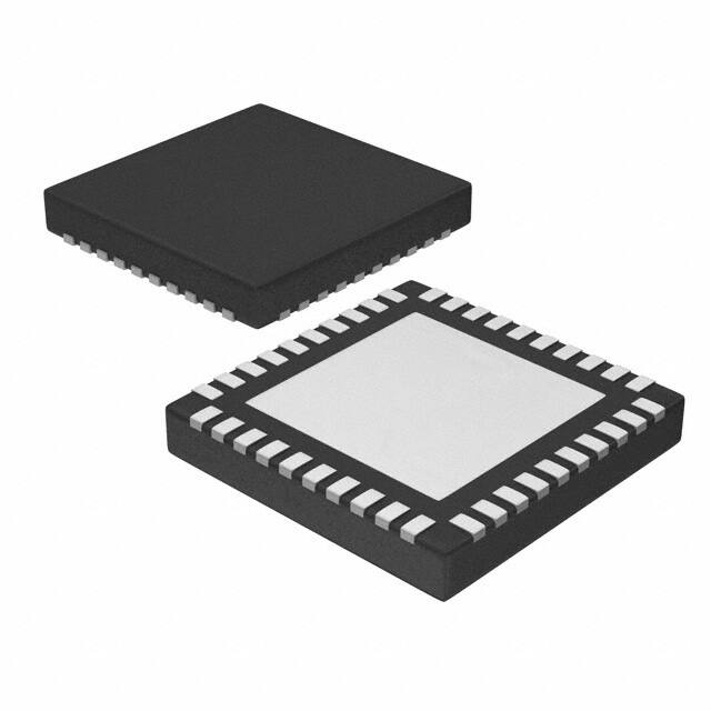


 工商网监
湘ICP备2023018690号
工商网监
湘ICP备2023018690号
