MSP430 Gang Programmer (MSP-GANG430)
User's Guide
Literature Number: SLAU101Q
March 2003 – Revised November 2011
�2
SLAU101Q – March 2003 – Revised November 2011
Submit Documentation Feedback
Copyright © 2003–2011, Texas Instruments Incorporated
�Contents
....................................................................................................................................... 7
Introduction, Installation, and Setup ...................................................................................... 9
1.1
Introduction ................................................................................................................. 10
1.2
Software Installation ....................................................................................................... 10
1.3
Hardware Installation ...................................................................................................... 11
Operation ......................................................................................................................... 13
2.1
Programming MSP430 Flash or FRAM Devices Using the GUI .................................................... 14
2.1.1 Procedure .......................................................................................................... 14
2.1.2 Description of the MSP-GANG430 GUI ....................................................................... 16
2.1.3 Status Messages ................................................................................................. 17
2.1.4 Error Messages ................................................................................................... 18
2.1.5 Description of the Gang430.ini File ............................................................................ 19
2.1.6 Target Connector Functional Check ........................................................................... 20
2.2
Programming MSP430 Flash or FRAM Devices in Stand-Alone Mode ............................................ 21
2.3
Programming MSP430 Flash or FRAM Devices With User-Configured UART Handler ......................... 21
2.4
Programming the MSP430 Devices With GANG430.DLL ........................................................... 21
Firmware .......................................................................................................................... 23
3.1
Commands ................................................................................................................. 24
3.2
Firmware Interface Protocol .............................................................................................. 24
3.3
Synchronization Sequence ............................................................................................... 24
3.4
Data Frame ................................................................................................................. 24
3.4.1 Frame Structure .................................................................................................. 25
3.4.2 Checksum ......................................................................................................... 25
3.5
Detailed Description of Commands ..................................................................................... 27
3.5.1 General ............................................................................................................ 27
3.5.2 Load Parameters ................................................................................................. 27
3.5.3 Start ................................................................................................................ 28
3.5.4 Transmit Diagnostic .............................................................................................. 28
3.5.5 Erase Image ....................................................................................................... 28
3.5.6 Load Image Block ................................................................................................ 29
3.5.7 Write Target Selective ........................................................................................... 29
3.5.8 Read Target Selective ........................................................................................... 29
3.5.9 Set Target VCC ..................................................................................................... 29
3.5.10 Load Image Checksum ......................................................................................... 29
3.5.11 Select Baud Rate ................................................................................................ 30
3.5.12 Execute Self Test ................................................................................................ 31
3.5.13 Set Signals ....................................................................................................... 31
3.5.14 Select Image ..................................................................................................... 31
3.5.15 Firmware Commands ........................................................................................... 31
Dynamic Link Library GANG430.DLL ................................................................................... 33
4.1
GANG430.DLL Description ............................................................................................... 34
4.2
Return Values/Error Codes From GANG430.DLL .................................................................... 54
Hardware .......................................................................................................................... 55
5.1
Specifications .............................................................................................................. 56
Preface
1
2
3
4
5
SLAU101Q – March 2003 – Revised November 2011
Submit Documentation Feedback
Copyright © 2003–2011, Texas Instruments Incorporated
Contents
3
�www.ti.com
5.2
5.3
5.4
5.5
5.6
5.7
6
Schematics
6.1
6.2
A
Programming Times vs Code Size for the Gang Programmer ......................................................
Recommendations for Target Connections ............................................................................
MSP-GANG430 Target Connector Signals ............................................................................
MSP-GANG430 Schematics .............................................................................................
MSP-GANG430 Component Locations .................................................................................
Gang_Exp Target Expansion Board Layout ...........................................................................
....................................................................................................................... 65
Schematics ................................................................................................................. 66
Hardware Revision History ............................................................................................... 72
Hex File Formats
A.1
A.2
56
57
57
61
62
63
............................................................................................................... 73
Intel Hex Object Format .................................................................................................. 74
TI-txt File Format .......................................................................................................... 75
............................................................................................... 77
........................................................................................................................ 78
C
Preproduction Checklist ..................................................................................................... 81
Document Revision History ......................................................................................................... 83
B
Frequently Asked Questions
B.1
4
FAQs
Contents
SLAU101Q – March 2003 – Revised November 2011
Submit Documentation Feedback
Copyright © 2003–2011, Texas Instruments Incorporated
�www.ti.com
List of Figures
1-1.
MSP-GANG430 Gang Programmer..................................................................................... 12
2-1.
MSP-GANG430 GUI ...................................................................................................... 15
5-1.
25-Pin Sub-D at MSP-GANG430 ........................................................................................ 58
5-2.
14-Pin Connector at End of Interconnect Cable ....................................................................... 58
5-3.
Signal Connections for 4-Wire JTAG Communication ................................................................ 60
5-4.
Signal Connections for 2-Wire JTAG Communication (SpyBiWire)
5-5.
MSP-GANG430 Component Locations ................................................................................. 62
5-6.
Gang_Exp Layout ......................................................................................................... 63
6-1.
MSP-GANG430 Schematic (1 of 5) ..................................................................................... 66
6-2.
MSP-GANG430 Schematic (2 of 5) ..................................................................................... 67
6-3.
MSP-GANG430 Schematic (3 of 5) ..................................................................................... 68
6-4.
MSP-GANG430 Schematic (4 of 5) ..................................................................................... 69
6-5.
MSP-GANG430 Schematic (5 of 5) ..................................................................................... 70
6-6.
MSP-GANG430 Expansion Board Schematic ......................................................................... 71
A-1.
Intel Hex Object Format .................................................................................................. 74
................................................
61
List of Tables
2-1.
Function Buttons and Descriptions ...................................................................................... 16
2-2.
Status Messages .......................................................................................................... 17
2-3.
Error Messages ............................................................................................................ 18
2-4.
Values for MiscErrors ..................................................................................................... 20
2-5.
Control Bit Definitions for Target Connector Pins ..................................................................... 20
3-1.
..................................................................................
Return Values/Error Codes ..............................................................................................
MSP-GANG430 Hardware Specifications ..............................................................................
MSP-GANG430 Target Connector Signal Functions .................................................................
MSP-GANG430 Signal Levels ...........................................................................................
Preproduction Checklist for the Gang Programmer ...................................................................
4-1.
5-1.
5-2.
5-3.
C-1.
Data Frame of Firmware Commands
SLAU101Q – March 2003 – Revised November 2011
Submit Documentation Feedback
Copyright © 2003–2011, Texas Instruments Incorporated
List of Figures
26
54
56
59
59
81
5
�All trademarks are the property of their respective owners.
6
List of Tables
SLAU101Q – March 2003 – Revised November 2011
Submit Documentation Feedback
Copyright © 2003–2011, Texas Instruments Incorporated
�Preface
SLAU101Q – March 2003 – Revised November 2011
Read This First
About This Manual
This user’s guide documents the MSP430 gang programmer MSP-GANG430 .
How to Use This Manual
This document contains the following chapters:
• Chapter 1 – Introduction, Installation, and Setup
• Chapter 2 – Operation
• Chapter 3 – Firmware
• Chapter 4 – Dynamic Link Library GANG430.DLL
• Chapter 5 – Hardware
• Chapter 6 – Schematics
Information About Cautions and Warnings
This book may contain cautions and warnings.
CAUTION
This is an example of a caution statement.
A caution statement describes a situation that could potentially damage your
software or equipment.
WARNING
This is an example of a warning statement.
A warning statement describes a situation that could potentially
cause harm to you.
The information in a caution or a warning is provided for your protection. Please read each caution and
warning carefully.
If You Need Assistance...
Support for the MSP430 device and the MSP-GANG430 is provided by the Texas Instruments Product
Information Center (PIC). Contact information for the PIC can be found on the Texas Instruments web site
at www.ti.com. Additional device-specific information can be found on the MSP430 web site at
www.ti.com/msp430.
SLAU101Q – March 2003 – Revised November 2011
Submit Documentation Feedback
Copyright © 2003–2011, Texas Instruments Incorporated
Read This First
7
�8
Read This First
SLAU101Q – March 2003 – Revised November 2011
Submit Documentation Feedback
Copyright © 2003–2011, Texas Instruments Incorporated
�Chapter 1
SLAU101Q – March 2003 – Revised November 2011
Introduction, Installation, and Setup
This chapter introduces the MSP-GANG430 and guides you through the installation of the software and
hardware.
Topic
1.1
1.2
1.3
...........................................................................................................................
Page
Introduction ...................................................................................................... 10
Software Installation .......................................................................................... 10
Hardware Installation ......................................................................................... 11
SLAU101Q – March 2003 – Revised November 2011
Submit Documentation Feedback
Copyright © 2003–2011, Texas Instruments Incorporated
Introduction, Installation, and Setup
9
�Introduction
1.1
www.ti.com
Introduction
The MSP-GANG430 is an MSP430 device programmer that can program up to eight identical MSP430
flash or FRAM devices at the same time. The MSP-GANG430 connects to the host PC using a standard
RS232 serial connection. The MSP-GANG430 provides flexible device programming options as described
in Chapter 2.
The MSP-GANG430 is not a gang programmer in the traditional sense; i.e., there are not eight sockets
provided to program the target devices. Instead, the MSP-GANG430 is designed to connect to the target
devices in-circuit (i.e., the target devices are mounted in the final circuit/system). The MSP-GANG430
accesses the target devices using connectors to the JTAG signals.
Chapter 6 contains a schematic that shows how the signals from the MSP-GANG430 can be brought out
to each of the target devices via an MSP430-standard JTAG connector. The circuit could easily be
modified to connect the signals to the target device pins directly (via a socket) if a traditional gang
programmer is desired.
The MSP-GANG430 is provided with an expansion board that implements the interconnections between
the MSP-GANG430 and multiple target devices. Eight cables are provided that connect the expansion
board to eight target devices (via a JTAG connector).
1.2
Software Installation
Always use the latest software version, which can be downloaded from the MSP430 web site at
www.msp430.com.
To install the MSP-GANG430 software:
1. Insert the MSP430 CD-ROM into the CD-ROM drive of the computer. Setup automatically opens the
default browser of the computer and displays the MSP430 start page.
If the start page does not open automatically, open the file index.htm located in the root directory of the
CD-ROM using a web browser. The MSP430 start page is displayed in the browser window.
2. Select Tools & Software.
3. Select MSP-GANG430 Gang Programmer.
4. Select Save this program to disk under the File Download options and click OK. A Save As dialog is
displayed.
5. Using the Save As dialog, save the GANG430_Rxxx.exe program to the computer. Make a note of the
directory path to this file.
6. Navigate to this file (GANG430_Rxxx.exe) and run it. A welcome message is displayed on the screen.
7. The setup program guides you through the installation process. Follow the setup instructions on the
screen.
8. On completion of the setup program execution, the MSP-GANG430 program icons are created in the
selected folder. Click on the GANG430 Read Me First icon to obtain important information about the
MSP-GANG430 hardware and software.
9. The appropriate program group and icons are added to the Windows desktop.
10. To start the MSP-GANG430 software, click the GANG430 icon in the selected program group (the
default program group is ADT430).
10
Introduction, Installation, and Setup
SLAU101Q – March 2003 – Revised November 2011
Submit Documentation Feedback
Copyright © 2003–2011, Texas Instruments Incorporated
�Hardware Installation
www.ti.com
1.3
Hardware Installation
To install the MSP-GANG430 hardware:
1. Connect the MSP-GANG430 to the serial port (COM1 to COM15 or extension board) of the PC using
the 9-pin Sub-D connector.
2. Connect an external power supply to the MSP-GANG430. The voltage of the power supply must be
between 9 V and 15 V dc and must be capable of providing a minimum current of 300 mA. The center
post of the power supply connector on the MSP-GANG430 is the positive-voltage terminal.
The power supply connection status is indicated by the yellow system LED on the MSP-GANG430.
3. Attach the expansion board to the 25-pin Sub-D connector on the MSP-GANG430. The expansion
board provides connectivity for up to eight targets, using the included 14-pin cables. The target
MSP430 flash or FRAM devices can be in stand-alone sockets or can be on an application’s PCB, and
they are accessed via the JTAG signals.
NOTE:
Maximum Signal Path Length: 60 cm
The maximum length of the signal path between the 25-pin Sub-D connector on the
MSP-GANG430 and a target device is 60 cm. If cables between the programmer and targets
are longer than 20 cm, serial resistors of 100 Ω should be inserted on signals TCK and TMS
on the expansion board. TCK is on pin 4 and TMS is on pin 3 of the 25-pin Sub-D connector.
4. The MSP-GANG430 provides the selected power-supply voltage VCC (VCC_MSP on pins 7 and 14 of
the 25-pin Sub-D target connector; pin 2 on the 14-pin cable) to the target devices in application PCBs.
A maximum total current of 150 mA can be provided by the programmer to the targets.
When an external supply voltage VCC is used for the target systems, it also should be connected to the
sense input pin (MSP_VCC_IN on pin 15 of the 25-pin Sub-D target connector; pin 4 on the 14-pin
cable) of the programmer. This connection allows the integrated level shifters to match the target JTAG
signal levels with the external supply voltage.
If the expander PCB (25-pin Sub-D to 8 x 14-pin header) is used, the external supply voltage must be
connected to pin 4 of the 14-pin header at position 1.
CAUTION
When an external supply voltage is used for the target systems, it is important
to disconnect VCC_MSP from the targets to avoid power-supply conflicts that
could potential damage the MSP-GANG430 and the targets. Connect the
external supply voltage to MSP_VCC_IN.
It is not possible to simultaneously use the MSP-GANG430 with targets
powered by the MSP-GANG430 and with targets powered by an external
supply.
SLAU101Q – March 2003 – Revised November 2011
Submit Documentation Feedback
Copyright © 2003–2011, Texas Instruments Incorporated
Introduction, Installation, and Setup
11
�Hardware Installation
www.ti.com
Power
supply
OK
1
2
3
4
5
6
7
8
MSP430 Gang Programmer
MSP-GANG430
MODE
TARGET
RS232
8-15V
300 mA
ERR
START
TI
JTAG connector
for eight
MSP430 devices
RS232
from
PC
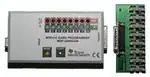
Figure 1-1. MSP-GANG430 Gang Programmer
12
Introduction, Installation, and Setup
SLAU101Q – March 2003 – Revised November 2011
Submit Documentation Feedback
Copyright © 2003–2011, Texas Instruments Incorporated
�Chapter 2
SLAU101Q – March 2003 – Revised November 2011
Operation
This chapter describes how to program MSP430 flash or FRAM devices using the MSP-GANG430.
Topic
2.1
2.2
2.3
2.4
...........................................................................................................................
Programming MSP430 Flash or FRAM Devices Using the GUI ................................
Programming MSP430 Flash or FRAM Devices in Stand-Alone Mode ......................
Programming MSP430 Flash or FRAM Devices With User-Configured UART
Handler ............................................................................................................
Programming the MSP430 Devices With GANG430.DLL .........................................
SLAU101Q – March 2003 – Revised November 2011
Submit Documentation Feedback
Copyright © 2003–2011, Texas Instruments Incorporated
Operation
Page
14
21
21
21
13
�Programming MSP430 Flash or FRAM Devices Using the GUI
2.1
www.ti.com
Programming MSP430 Flash or FRAM Devices Using the GUI
2.1.1 Procedure
Use the following sequence to start the GUI and program MSP430 flash or FRAM devices using the
MSP-GANG430.
1. Connect the MSP-GANG430 hardware and the targets as described in Section 1.3.
2. Click on the GANG430 icon located in the program group specified during installation of the software
(the default group is ADT430). The MSP430 Gang Programmer GUI is displayed on the screen (see
Figure 2-1).
If a Firmware Update dialog appears, see FAQ #3 in Section B.1. The status line in the GUI displays
the message "MSP-GANG430 Gang Programmer connected." If this message is not displayed, check
the COM Port selection in the communication settings and the MSP-GANG430 connections.
3. Select the required device using the Group and Type menu.
4. Select the object code file(s) to be programmed into the device(s) using the File Names menu. The
formats supported for the object code file are TI TXT (.txt) and Intel hex (.a43, .hex, .int).
5. Use the Load Image button to download the object code file and its checksum to the MSP-GANG430.
The data is written to an internal memory called the image buffer.
6. Select the supply voltage using the Supply Voltage menu.
7. Select the options in Main Process as required.
8. Click on the Start button in the Main Process section to start the programming operation. The progress
and completion of the operation are displayed in the Status section.
Before the gang programming operation starts, a reset of all targets is performed. The duration of the
reset pulse and the delay after reset are specified by Settling Time. The reset feature is available on
hardware V1.30 and later.
14
Operation
SLAU101Q – March 2003 – Revised November 2011
Submit Documentation Feedback
Copyright © 2003–2011, Texas Instruments Incorporated
�Programming MSP430 Flash or FRAM Devices Using the GUI
www.ti.com
Figure 2-1. MSP-GANG430 GUI
SLAU101Q – March 2003 – Revised November 2011
Submit Documentation Feedback
Copyright © 2003–2011, Texas Instruments Incorporated
Operation
15
�Programming MSP430 Flash or FRAM Devices Using the GUI
www.ti.com
2.1.2 Description of the MSP-GANG430 GUI
Table 2-1 describes the function buttons and option settings in the MSP-GANG430 GUI.
Table 2-1. Function Buttons and Descriptions
Button Group
Functions
Start
Executes the function(s) selected in Main Process
Erase
Erases the target’s flash memories as selected on the panel Erase/Check
Erase
Erase Check
Checks if the target’s memories are erased as selected on the panel
Erase/Check Erase
Program
Programs the image buffer into the target’s flash or FRAM memory
Verify
Compares the target’s flash or FRAM memory and the image buffer
Secure Device
Makes MSP430 devices secure after successful completion of the selected
operations (permanently disables device access through JTAG)
Supplied by
Programmer
The connected targets are powered by the MSP-GANG430 via VCC_MSP
pin.
Switch Vcc Off
The supply voltage provided by the VCC_MSP pin is switched off after
programming the targets.
Supply Voltage
Selects the voltage supplied to the targets
Settling Time
Specifies the time to allow the target capacitors to fully charge
Load Image
Loads the selected object code file into the image buffer
Group
Selects the group (family) device to be programmed belongs to
Type
Select the target device
Device Information
Shows memory details of the selected device type
File Names
Selects one or two files containing the object code. If two files are selected,
their contents will be merged during download.
Main Memory
Select to specify that the main memory should be erased or checked
according to setting in group Main Process.
Info Memory
Select to specify that the info memory should be erased or checked according
to setting in group Main Process.
Protected Info
Select to specify that the protected info memory (INFO A) should be erased
and/or checked according to setting in group Main Process.
BSL Memory
Select to specify that the BSL memory should be erased or checked
according the settings in group Main Process
Execute
Starts the operation that is selected in Category
H/W Self Test
Initiates hardware self test
All green LEDs on = test pass. All red LEDs on = test fail.
Update Firmware
Updates MSP-GANG430 firmware with the firmware update file
Read out Target
Reads out exclusively one of eight target modules
Erase Image
Erases the image buffer
Target Connector (Test)
Sets the selected pin on the 25-pin target connector of the MSP-GANG430
Use SpyBiWire
Check this option if the 2-wire SpyBiWire interface should be used for device
operation. This option is not available for all devices.
Note: The 2-wire SpyBiWire interface operation is slower than the regular
4-wire JTAG.
COM port
Selects the PC serial port used to communicate with the MSP-GANG430
Baud Rate
Selects the baud rate of the serial port
System Menu Mode
The System Menu is displayed by clicking on the icon at the upper left corner
of GUI (or {Alt} and {Space} pressed together).
Lock Settings
Locks all settings on the GUI. Only the Start button, Result group box, and
Status group box are displayed. Other group boxes are hidden.
Unlock Settings
The locked settings and the hidden group boxes are enabled.
Help
Opens the user help window
About Gang
Programmer
Displays the desktop application software and firmware version and filename
information (or press F1)
Main Process
Target Power
Target Program/Device
Erase/Check Erase
Maintenance
JTAG
Communication Settings
System Menu
16
Operation
Description
SLAU101Q – March 2003 – Revised November 2011
Submit Documentation Feedback
Copyright © 2003–2011, Texas Instruments Incorporated
�Programming MSP430 Flash or FRAM Devices Using the GUI
www.ti.com
2.1.3 Status Messages
Table 2-2 shows the status messages that can be displayed in the MSP-GANG430 GUI during operation.
Table 2-2. Status Messages
Status Type
Status Message
Executing main process...
Erasing image buffer...
Loading image buffer...
Loading checksum of image buffer...
Progress
Erasing firmware section...
Loading firmware section...
Initializing firmware...
Changing baud rate...
Executing self test...
Setting signals at target connector...
Operation successful
System
MSP-GANG430 gang programmer connected.
Result of the operation: See the result section.
Setting
Maintenance
COM port settings modified. MSP-GANG430 gang programmer connected.
Target power settings modified
Operation successful
Selftest passed
SLAU101Q – March 2003 – Revised November 2011
Submit Documentation Feedback
Copyright © 2003–2011, Texas Instruments Incorporated
Operation
17
�Programming MSP430 Flash or FRAM Devices Using the GUI
www.ti.com
2.1.4 Error Messages
Table 2-3 shows the error messages that can be displayed in the MSP-GANG430 GUI when an error
occurs during operation.
Table 2-3. Error Messages
Error Type
Error Message
ERROR: Unable to read Target!
ERROR: Unable to open COM port − already in use?
Communication
ERROR: Unable to close COM port!
ERROR: Synchronization failed. Programmer connected?
ERROR: Time out during operation − Correct COM port selected?
ERROR: Communication − Frame has errors!
ERROR: Select baud rate command not accepted!
WARNING: Target voltage too low for erase / program operation! Set to > 2.7-V.
WARNING: Could not set target voltage − Externally supplied?
ERROR: Value wrong or out of range!
ERROR: Selected file is of unrecognizable format!
ERROR: Selected file is not a firmware update file!
ERROR: Firmware section cannot be erased!
ERROR: Unable to load firmware. Correct file format?
ERROR: Unable to refresh gang programmer system parameters!
Setting System
ERROR: Unable to load Image buffer! Image buffer erased? Correct file format?
ERROR: Result of operation not received!
FATAL ERROR: Image memory corrupted or erased!
ERROR: Unexpected end of file!
ERROR: File contains invalid record!
ERROR: Wrong target device connected!
ERROR: Image range XXXX−YYYY placed outside of existing memory
ERROR: No target device connected
ERROR: File(s) contains already specified data (code overwritten)
General error!
ERROR: Self test failed – No access to one ore more image buffer devices!
ERROR: Self test failed − No JTAG access to one or more target channels!
Maintenance
ERROR: Self test failed − Target voltage generator (VCCT) does not work properly!
ERROR: Self test failed – System voltage (VCC) not in range!
ERROR: Self test failed − Blow fuse voltage (VPP) not in range!
ERROR: Unable to open file!
Windows
ERROR: Error during file I/O!
ERROR: Unable to open INI file!
18
Operation
SLAU101Q – March 2003 – Revised November 2011
Submit Documentation Feedback
Copyright © 2003–2011, Texas Instruments Incorporated
�Programming MSP430 Flash or FRAM Devices Using the GUI
www.ti.com
2.1.5 Description of the Gang430.ini File
The Gang430.ini file contains the MSP-GANG430 default settings and the most recently used GUI
settings.
2.1.5.1
Section [System]
The most recently used settings of the MSP-GANG430 GUI are stored in the Gang430.ini file when the
GUI application exits. This information is stored under the [System] section of the file. There are few
entries in this section that cannot be changed via the GUI.
JtagSpeed = 0 (default value is 0)
Set JtagSpeed = 1 to make the JTAG connection slower. This can be used for quality testing of the cable
between target devices and the MSP-GANG430.
VerifyMarginal = 0 (default value is 0)
Set VerifyMarginal = 0 to avoid the marginal check on devices with the marginal read feature. It can be
used to reduce the verification time. For more information, see the MSP430x2xx Family User's Guide or
MSP430x4xx Family User's Guide.
2.1.5.2
Section [User]
The initial settings for the following parameters are in the [User] section and may be modified by the user.
CaptionIndexed = 0 (default). The caption of the MSP-GANG430 GUI in the default state is MSP430 Gang
Programmer.
CaptionIndexed = 1. The caption is extended with a suffix [n] to allow multiple-instance operation for
programming in automated production environment that uses caption titles for process control. The suffix n
represents the unique COMn port number for that instance. For example, for COM3, the caption is
displayed as MSP430 Gang Programmer [3].
2.1.5.3
Section [Timing]
The [Timing] section shows the approximate time, in milliseconds, that has elapsed for various operations
of the MSP-GANG430. The parameters under this section are updated after successful completion of the
associated operations. The information on the elapsed time is useful for development and setup. The
parameter that is most often useful is the time taken to complete a gang programming cycle, which is
reported in the TimeGangProg key in this section.
2.1.5.4
Section [Diagnostic]
The [Diagnostic] section is useful for automatic production using the MSP-GANG430. During gang
programming operation, Busy = 1. After completion of the operation, the information in the Result group
box in the GUI is also listed in this section for the following: Connected, EraseChecked, Verified,
SecureDevice, OverAll, and MiscErrors, if any. A Busy = 0 terminates that process and the diagnostics
can be read from the .ini file.
For example:
OverAll = 239 (0xEF) indicates that all channels except channel 5 were successfully processed
(channel 1 represents the LSB, channel 8 represents the MSB of a byte).
NOTE: When MiscErrors is nonzero, the diagnostic values are not valid for evaluation. Possible
values for MiscErrors are shown in Table 2-4.
SLAU101Q – March 2003 – Revised November 2011
Submit Documentation Feedback
Copyright © 2003–2011, Texas Instruments Incorporated
Operation
19
�Programming MSP430 Flash or FRAM Devices Using the GUI
www.ti.com
Table 2-4. Values for MiscErrors
MiscErrors
Description
0
Operation successful
1
FATAL ERROR: Image memory could be corrupted or erased
11
ERROR: Main process parameters not yet set
16
ERROR: Could not set target voltage (VCCT) − MSP_VCC_IN pin connected?
2.1.6 Target Connector Functional Check
The MSP-GANG430 GUI diagnostics support a functional check of the target connector pins. The
functional check is invoked by selecting the Target Connector category in the Maintenance group box, and
clicking the Execute button with the appropriate Set Signals defined. The Set Signals value is the decimal
value that represents the combination of the appropriate control bits. The defined pin’s signal level is
available for measurement after execution of the functional check. The signal levels remain unchanged
until another configuration is set. The target connector functional check always must be terminated by
executing the End of Check setting (0x8000 = 32768) or by executing an hardware self test to initialize the
MSP-GANG430. Table 2-5 shows the details of the control bits.
Table 2-5. Control Bit Definitions for Target Connector Pins
Bit
Pin Function and Level
Signal Level
Connector Pins
0x0000
Select TDO/TDI1
–
1, 8
0x0001
Select TDO/TDI2
–
9
0x0002
Select TDO/TDI3
–
10
0x0003
Select TDO/TDI4
–
11
0x0004
Select TDO/TDI5
–
12
0x0005
Select TDO/TDI6
–
13
0x0006
Select TDO/TDI7
–
25
0x0007
Select TDO/TDI8
–
24
0x0008
Logic level at TDO/TDIx pin
VCC or 0
1, 8–13, 25, 24
Logic level at TDI/VPP pin
VCC/VPP or 0
2
0x0010
Logic level at TCK pin
VCC or 0
4
0x0020
Logic level at TMS pin
VCC or 0
3
0x0040
Logic level at TEST/VPP pin
VCC – 0.25 V or 0
17
0x0080
Logic level at TDI/VPP pin
VCC or 0
2
0x0100
VCC on/off at VCC_MSP pin
VCC or 0
7, 14
0x0200
VPP on/off at TDI/VPP pin, overwrites bit 0x0080
VPP or 0
2
0x0400
VPP on/off at TEST/VPP pin
VPP or 0
17
0x0800
RESET activate/deactivate on RST pin
VCC or 0
6
0x7000
Reserved
0x8000
End of check, reinitialize MSP-GANG430
Initial
All
Example 1
To check the logic-high level on TDO/TDI3 and VPP voltage level on TEST/VPP:
Enter 0x040A (0x0002 + 0x0008 + 0x0400) into Set Signal and click Execute.
The VCC at pin 10 and VPP at pin 17 can be measured now. All other pins remain at 0 V. The connector
case is electrically grounded, as are pins 19 to 23.
20
Operation
SLAU101Q – March 2003 – Revised November 2011
Submit Documentation Feedback
Copyright © 2003–2011, Texas Instruments Incorporated
�Programming MSP430 Flash or FRAM Devices in Stand-Alone Mode
www.ti.com
Example 2
To let free run target 3 programmed via SpyBiWire (2-wire mode):
Select TDO/TDI3 = 0x0002
Logic level at TDO/TDIx = 0x0008
VCC on at VCC_MSP pin = 0x0100
Enter 0x010A (0x0002 + 0x0008 + 0x0100) into Set Signal and click Execute.
2.2
Programming MSP430 Flash or FRAM Devices in Stand-Alone Mode
The MSP-GANG430 supports a stand-alone mode of programming the target MSP430 flash or FRAM
devices.
The programming options for the MSP-GANG430 while it operates in stand-alone mode are configured
using the GUI. When the Start button in Main Process is clicked, all selected options are downloaded into
the flash or FRAM memory of the MSP-GANG430. Once the download is complete, the MSP-GANG430
can be disconnected from the PC and used stand-alone to program the target devices. The Start button
on the MSP-GANG430 operates the same as the Start button of the GUI. Note that after performing
additional MSP-GANG430 operations using the GUI, the options to be used for stand-alone programming
need to be re-downloaded into the flash or FRAM memory of the MSP-GANG430 by pressing of the Start
button of the GUI. Note that after performing additional MSP-GANG430 operations using the GUI, the
options to be used for stand-alone programming need to be downloaded again into the flash or FRAM
memory of the MSP-GANG430. Progress of the operation in stand-alone mode is indicated by the flashing
yellow LED.
The result status is represented by the rows of green and red LEDs on the MSP-GANG430. For each
channel, a green LED indicates a successful operation, and a red LED indicates a failed operation. If both
red and green LEDs are off for a channel, the target device connected to that channel is not accessible or
there is no target device.
To start the hardware self test of the MSP-GANG430 while in stand-alone mode, press and hold the Start
key for more than three seconds. The progress of the test is indicated by alternately flashing green and
red LEDs in groups of four. If the self test passes, all eight green LEDs are on. Any other combination of
the LEDs indicates that the self test failed.
NOTE: If the GANG430.DLL is used for configuration of MSP-GANG430 in stand-alone mode, the
MSP-GANG430 works with image #0 (default) after power on. Thus, the programming
options and the program code should be downloaded into image #0. This is not relevant
when using the GUI gang430.exe, because it uses only image #0.
2.3
Programming MSP430 Flash or FRAM Devices With User-Configured UART Handler
The MSP-GANG430 programmer supports programming the MSP430 flash or FRAM devices using
generic firmware commands. The generic firmware commands and protocol are described in Chapter 3.
2.4
Programming the MSP430 Devices With GANG430.DLL
The MSP-GANG430 programmer supports programming the MSP430 flash or FRAM devices by using
DLL functions. The usage of the DLL functions and their prototypes (calling conventions) are described in
Chapter 4.
SLAU101Q – March 2003 – Revised November 2011
Submit Documentation Feedback
Copyright © 2003–2011, Texas Instruments Incorporated
Operation
21
�22
Operation
SLAU101Q – March 2003 – Revised November 2011
Submit Documentation Feedback
Copyright © 2003–2011, Texas Instruments Incorporated
�Chapter 3
SLAU101Q – March 2003 – Revised November 2011
Firmware
This chapter describes the firmware commands and protocol for controlling the MSP-GANG430 via its
RS-232 serial communication interface.
Topic
3.1
3.2
3.3
3.4
3.5
...........................................................................................................................
Commands .......................................................................................................
Firmware Interface Protocol ................................................................................
Synchronization Sequence .................................................................................
Data Frame .......................................................................................................
Detailed Description of Commands .....................................................................
SLAU101Q – March 2003 – Revised November 2011
Submit Documentation Feedback
Copyright © 2003–2011, Texas Instruments Incorporated
Firmware
Page
24
24
24
24
27
23
�Commands
3.1
www.ti.com
Commands
The MSP-GANG430 can be controlled via firmware commands received through its RS-232 serial port.
The following firmware commands are supported:
• Load Parameters
• Start
• Transmit Diagnostics
• Erase Image
• Load Image Block
• Load Image Checksum
• Erase Firmware
• Load Firmware Block
• Finalize Firmware
• Select Baud Rate
• Execute Self Test
• Set Signals (at target connector)
• Read Target Selective
• Write Target Selective
• Set Target VCC
• Select Image
3.2
Firmware Interface Protocol
The MSP-GANG430 supports the following UART communication protocol:
• Baud rates from 9600 to 115200 baud in half duplex mode. The default baud rate at startup is 115200
baud, which is the recommended baud rate.
• One start bit, eight data bits, even parity bit, and one stop bit
• Software handshake by (not)acknowledge character
3.3
Synchronization Sequence
To synchronize with the MSP-GANG430, the host serial handler transmits a SYNC character (0x80) to the
MSP-GANG430. The MSP-GANG430 acknowledges successful reception of the SYNC by responding
with a DATA_ACK character (0x90). If the SYNC is not received correctly, a DATA_NAK character (0xA0)
is sent back. This sequence is required to establish the communication channel and/or react immediately
to line faults.
NOTE: The synchronization character is not part of the data frame described in Section 3.4.
3.4
Data Frame
The data frame format follows the TI MSP430 serial standard protocol (SSP) rules, extended with a
preceding synchronization sequence (SS), as described in Section 3.3. The MSP-GANG430 is considered
the receiver in Table 3-1.
The redundancy of some parameters results from the adaptation of the SSP or to save boot ROM space.
24
Firmware
SLAU101Q – March 2003 – Revised November 2011
Submit Documentation Feedback
Copyright © 2003–2011, Texas Instruments Incorporated
�Data Frame
www.ti.com
3.4.1 Frame Structure
The data frame format of the firmware commands is shown in Table 3-1.
• The first eight bytes (HDR through LH) are mandatory (– represents dummy data).
• Data bytes D1 to Dn are optional.
• Two bytes (CKL and CKH) for checksum are mandatory.
• Acknowledge done by the MSP-GANG430 is mandatory except with the Transmit Diagnostic
command.
3.4.2 Checksum
The 16-bit (2-byte) checksum is calculated over all received/transmitted bytes, B1 to Bn, in the data frame
except the checksum bytes themselves by XORing words (two successive bytes) and inverting the result,
as shown in the following formulas.
CHECKSUM = INV [ (B1 + 256 × B2) XOR (B3 + 256 × B4) XOR … XOR ((Bn – 1) + 256 × Bn) ]
or
CKL = INV [ B1 XOR B3 XOR … XOR Bn–1 ]
CKH = INV [ B2 XOR B4 XOR … XOR Bn ]
The example of the frame Execute Self Test with checksum:
0x80 0x35 0x06 0x06 0x00 0x00 0x00 0x00 0x00 0x00 0x79 0xCC
SLAU101Q – March 2003 – Revised November 2011
Submit Documentation Feedback
Copyright © 2003–2011, Texas Instruments Incorporated
Firmware
25
�Data Frame
www.ti.com
Table 3-1. Data Frame of Firmware Commands
Received
MSPGANG430
Firmware
Command
(1) (2)
HDR
CMD
L1
L2
A1
A2
A3
A4
LL
LH
D1
D2...Dn
CKL
CKH
ACK
Load
Parameters
80
36
08
08
D1
D2
D3
D4
D5
D6
00
00
CKL
CKH
ACK
Start
80
31
06
06
00
00
–
–
00
00
00
00
CKL
CKH
ACK
Transmit
Diagnostic
80
32
04
04
00
00
–
–
00
00
–
–
CKL
CKH
–
GANG430
responds on
Transmit
Diagnostic
80
00
20
20
D1
D2
–
–
D3
D4
D5
D06...D20
CKL
CKH
–
Erase Image
80
33
06
06
00
00
–
–
00
00
00
00
CKL
CKH
ACK
Load Image
Block
80
34
n
n
A1
A2
A3
00
n–6
00
D1
D2...Dn–6
CKL
CKH
ACK
Load Image
Checksum
80
37
n
n
D1
D2
–
–
D3
D4
D5
D6...Dn
CKL
CKH
ACK
Execute Self
Test
80
35
06
06
00
00
–
–
00
00
00
00
CKL
CKH
ACK
Set Signals
80
30
04
04
D1
D2
–
–
D3
D4
–
–
CKL
CKH
ACK
Erase
Firmware
80
39
04
04
D1
D2
–
–
D3
D4
–
–
CKL
CKH
ACK
Load
Firmware
Block
80
3A
n
n
AL
AH
–
–
n–4
00
D1
D2...Dn–4
CKL
CKH
ACK
Finalize
Firmware
80
3B
04
04
00
00
–
–
00
00
–
–
CKL
CKH
ACK
Select Baud
Rate
80
38
06
06
D1
00
–
–
00
00
00
00
CKL
CKH
ACK
Write Target
Selective
80
3C
n
n
A1
A2
A3
00
n–6
00
D1
D2...Dn–6
CKL
CKH
ACK
Read Target
Selective
80
3D
08
08
A1
A2
A3
00
n
00
D1
D2
CKL
CKH
–
(1)
All numbers are bytes in hexadecimal notation. ACK is sent by the MSP-GANG430. The synchronization sequence (TX = 0x80,
RX = 0x90) is not part of the data frame. It must precede every frame.
(2)
HDR:
CMD:
L1, L2:
A1, A2,
A3:
LL, LH:
D1...Dn:
CLK,
CKH:
xx:
–:
ACK:
n:
26
Firmware
DATA_FRAME = 0x80 means data frame expected in accordance with TI MSP430
serial standard protocol (SSP).
Command identification
Number of bytes consisting of A1 through Dn. The valid values of these bytes are
restricted as follows: L1 = L2, L1 < 255, L1 even.
Block start address or erase (check) address or jump address LO/HI byte. The bytes
are combined to generate a 24-bit word as follows: Address = A3 × 0x10000 + A2 ×
0x100 + A1
Number of pure data bytes (maximum 250) or erase information LO/HI byte or block
length of erase check (maximum is 0xFFFF)
Data bytes
16-bit checksum LO/HI byte
Can be any data
No character (data byte) received/transmitted
The acknowledge character returned by the MSP-GANG430 can be either
DATA_ACK = 0x90 (frame was received correctly, command was executed
successfully) or DATA_NAK = 0xA0 (frame not valid (for example, wrong checksum,
L1 ≠ L2), command is not defined, is not allowed, or was executed unsuccessfully).
Number of bytes
SLAU101Q – March 2003 – Revised November 2011
Submit Documentation Feedback
Copyright © 2003–2011, Texas Instruments Incorporated
�Detailed Description of Commands
www.ti.com
Table 3-1. Data Frame of Firmware Commands (1)
Received
MSPGANG430
Firmware
Command
3.5
(2)
(continued)
HDR
CMD
L1
L2
A1
A2
A3
A4
LL
LH
D1
D2...Dn
CKL
CKH
ACK
GANG430
responds on
Read Target
Selective
80
00
n
n
D1
D2
–
–
D3
D4
D5
D6...Dn
CKL
CKH
–
Set Target
VCC
80
3E
04
04
D1
D2
–
–
D3
D4
–
–
CKL
CKH
ACK
Select Image
80
50
06
06
D1
00
–
–
00
00
00
00
CKL
CKH
ACK
Detailed Description of Commands
3.5.1 General
After the header byte HDR (0x80) and the command identification byte CMD, the frame length bytes L1
and L2 (which must be equal) hold the number of bytes following L2, excluding the checksum bytes CKL
and CKH.
Bytes A1, A2, A3, A4, LL, LH, and D1 to Dn are command specific. However, the checksum bytes CKL
(low byte) and CKH (high byte) are mandatory.
If the data frame is received correctly and the command execution is successful, the acknowledge byte
ACK is send back by the MSP-GANG430 set to DATA_ACK = 0x90. Incorrectly received data frames,
unsuccessful operations, and commands that are not defined are confirmed with a DATA_NAK = 0xA0.
The data frame should be sent to the MSP-GANG430 within one second after the synchronization
sequence (TX = 0x80, RX = 0x90).
3.5.2 Load Parameters
The Load Parameters command downloads to the MSP-GANG430 the information that the main process
needs for gang programming. It must be invoked before the first gang programming command. The
parameters are stored in the system flash memory.
Data bytes D1 to D6 specify the parameters, as follows:
D1: Flags for process control, in any combination
0x01: Executes erasure of info memory
0x02: Executes erasure of main memory
0x04: Executes erasure of protected info memory
0x07: Executes erasure of main and info memory (including protected info)
0x08: Executes programming of info memory
0x10: Executes programming of main memory
0x18: Executes programming of info and main memory
0x20: Executes verification of info and main memory
0x40: Makes MSP430 devices secure
0x80: Executes programming of RAM memory
D2: Flags for target supply voltage VCC_MSP
0x3F: Voltage in 100-mV steps (valid values are 18 to 36, and 0 for external supply)
0x80: Switch VCC_MSP off after programming
D3
0x01: Executes erase check of info memory
0x02: Executes erase check of main memory
0x04: Executes erase check of protected info memory
0x07: Executes erase check whole memory
SLAU101Q – March 2003 – Revised November 2011
Submit Documentation Feedback
Copyright © 2003–2011, Texas Instruments Incorporated
Firmware
27
�Detailed Description of Commands
www.ti.com
0x08: Use Spy-Bi-Wire JTAG interface
0x10: Use slower JTAG speed mode. Not applicable for Spy-Bi-Wire communication mode.
0x40: Verify targets additionally for marginal 1 and 0. For more information, see the MSP430x2xx
Family User's Guide or MSP430x4xx Family User's Guide.
D4:
0x01: Executes erasure of the BSL memory
0x02: Executes erase check of the BSL memory
0x04: Executes programming of the BSL memory
D5, D6: VCC_MSP settle time
Delay in milliseconds between switching VCC_MSP on and starting programming cycle. Valid
values are 1 to 0xFFFF (>65 s). D5 holds the LSB, and D6 holds the MSB.
Protected information memory segments can be treated in two ways:
• If the calibration data that was stored during factory testing is not needed, this segment can be
used as normal information memory segments, and D1 bit 0x04 should be set.
• If calibration data should be preserved, D1 bit 0x04 should be cleared to avoid erasing of the
protected information memory segment when normal information memory is erased.
3.5.3 Start
The Start command begins the gang programming cycle, using the operations defined with the Load
Parameters command. The result of the command execution can be determined using the Transmit
Diagnostic command described in Section 3.5.4.
3.5.4 Transmit Diagnostic
The Transmit Diagnostic command retrieves the result of the preceding gang programming command.
Data bytes D1 to D30 hold the parameters, as follows:
D1 to D5 give information about success of each target channel. The LSB represents channel 1, the
MSB represents channel 8.
D1: Channels that are connected to the programmer (device detected)
D2: Channels that passed the erase check successfully
D3: Channels that passed the verification successfully
D4: Channels that passed the device securing successfully, or are already secured
D5: Channels that passed all operations successfully
D6: Miscellaneous errors (see Section 2.1.5.4)
D7 to D8 are reserved.
D9 to D10 hold the hardware version number: D9 (MSByte), D10 (LSByte).
D11 to D12 hold the firmware version number: D11 (MSByte), D12 (LSByte).
D13 to D30 hold a zero-terminated character string representing the firmware file name; for example,
GANG430_100.TXT.
3.5.5 Erase Image
The Erase Image command erases the entire image memory and verifies the erasure.
28
Firmware
SLAU101Q – March 2003 – Revised November 2011
Submit Documentation Feedback
Copyright © 2003–2011, Texas Instruments Incorporated
�Detailed Description of Commands
www.ti.com
3.5.6 Load Image Block
The Load Image Block command loads the data bytes into the image buffer of the MSP-GANG430 and
verifies them.
D1 to Dn–4 contain the data bytes.
3.5.7 Write Target Selective
The Write Target Selective command loads the data bytes into one exclusively selected target flash or
FRAM memory and verifies them.
Before applying this operation, stable supply voltage at the targets is assumed (if not, use Set Target VCC
command and optionally wait for capacitor’s settle time).
D1: Target number (0 to 7)
D2: 0
D3 to Dn–4 contain the data bytes (start address and number of bytes must be even numbered).
3.5.8 Read Target Selective
The Read Target Selective command is used for any read access to the flash, FRAM, RAM or peripheral
module control registers at 0x0100 to 0x01FE of the selected target.
The 20-bit block start address is defined as:
Address = A3 × 0x10000 + A2 × 0x100 + A1
The 16-bit block length is defined in LL (low byte) and LH (high byte). Because pure data bytes are limited
to a maximum of 244, LH is always 0.
For this operation, stable supply voltage at the targets is necessary. If not, use Set Target VCC command
and wait for capacitor’s settle time, as required.
D1: Target number (0 to 7)
D2: 0
The GANG430 responds with the requested data block. No acknowledge character is necessary.
D1 to Dn contain the data bytes (start address and number of bytes must be even numbered).
3.5.9 Set Target VCC
The Set Target VCC command sets the VCC_MSP pin voltage of the programmer’s target connector to the
given value.
D1: Target supply voltage
0: VCC_MSP output voltage is equal to MSP_VCC_IN input voltage.
1: VCC_MSP output voltage is switched off.
2: VCC_MSP output voltage is same as loaded by the Load Parameters command.
18+: VCC_MSP is set in hundreds of millivolts (for example, D1 = 36 for 3.6 V).
3.5.10 Load Image Checksum
The Load Image Checksum command writes the checksums of all non-empty memory segments (Info_x,
main, RAM) and the memory model of the target device into the system flash memory. The gang
programmer uses the checksums to verify the correct download of data to the image buffer and the correct
programming of the target device.
On devices with protected information memory segments (for example, SegA on F2xxx devices), it can be
indicated if this segment should be excluded from erasure when the other information memory segments
are to be erased.
The number of parameters depends on the memory model of the selected device.
SLAU101Q – March 2003 – Revised November 2011
Submit Documentation Feedback
Copyright © 2003–2011, Texas Instruments Incorporated
Firmware
29
�Detailed Description of Commands
www.ti.com
Data bytes D1 to D4 hold the parameters, as follows:
D1:
0x80: VPP to TEST
0x00: VPP to TDI
D2: Combination of
0x01: Device is Spy-Bi-Wire capable
0x02: Device has X-CPU
D3: Device ID, corresponds to DevId in GANG430.ini file, LSByte
D4: Device ID, corresponds to DevId in GANG430.ini file, MSByte
D5: Byte 0x0D from ROM device ID, corresponds to DevIdxD
D6: Reserved, should be 0x00
For each memory segment of the device (main memory is treated as one segment), a set of 8 bytes
indicating memory type, start address, length, and checksum follows:
D7: Memory type
0x06: Calibration data
0x05: Protected Info
0x03: Main
0x02: Info
0x01: RAM
0x00: Terminates the list of memory segment descriptions
D8
0x01: Indicates that the memory segment is empty (= 0xFFFF)
0x00: Indicates that the memory segment is not empty
D9: Segment start address, bits 23 to 16
D10: Segment start address, bits 15 to 8
D11: Segment start address, bits 7 to 0
D12: Segment length, bits 23 to 16
D13: Segment length, bits 15 to 8
D14: Segment length, bits 7 to 0
D15: Checksum (PSA) for memory segment, LSByte
D16: Checksum (PSA) for memory segment, MSByte
The list must be terminated by a single byte containing 0x00.
D7 to D14 correspond to the MemDefx=... entries in the GANG430.INI File.
The pseudo signature analysis (PSA) is computed using the following algorithm (using the C language):
for (PSA = StartAddr - 2, i = 0; i < Length; i++) { if (PSA & 0x8000) PSA = ((PSA ^
0x0805)


 工商网监
湘ICP备2023018690号
工商网监
湘ICP备2023018690号
