®
OPA2541
Dual High Power
OPERATIONAL AMPLIFIER
FEATURES
DESCRIPTION
● OUTPUT CURRENTS TO 5A
● POWER SUPPLIES TO ±40V
● FET INPUT
The OPA2541 is a dual power operational amplifier
capable of operation from power supplies up to ±40V
and output currents of 5A continuous. With two monolithic power amplifiers in a single package it provides
unequaled functional density.
● ELECTRICALLY ISOLATED CASE
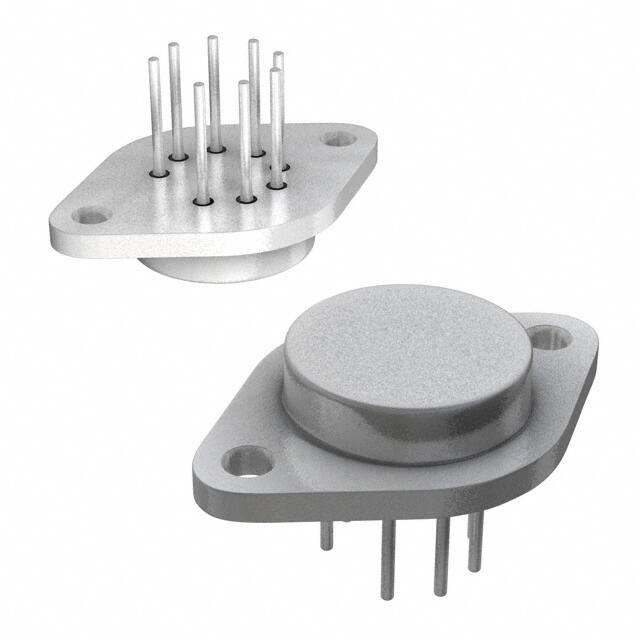
The industry-standard 8-pin TO-3 package is isolated
from all internal circuitry allowing it to be mounted
directly to a heat sink without insulators which degrade thermal performance. Internal circuitry limits
output current to approximately 6A.
APPLICATIONS
●
●
●
●
●
MOTOR DRIVER
SERVO AMPLIFIER
SYNCRO/RESOLVER EXCITATION
VOICE COIL DRIVER
BRIDGE AMPLIFIER
The OPA2541 is available in both industrial and
military temperature range versions.
● PROGRAMMABLE POWER SUPPLY
● AUDIO AMPLIFIER
+VS (2)
–In
(4, 8)
+In
(3, 7)
Out
(5, 1)
–VS (6)
International Airport Industrial Park • Mailing Address: PO Box 11400
Tel: (520) 746-1111 • Twx: 910-952-1111 • Cable: BBRCORP •
©
SBOS157
1987 Burr-Brown Corporation
• Tucson, AZ 85734 • Street Address: 6730 S. Tucson Blvd. • Tucson, AZ 85706
Telex: 066-6491 • FAX: (520) 889-1510 • Immediate Product Info: (800) 548-6132
PDS-768B
Printed in U.S.A. October, 1993
�SPECIFICATIONS
ELECTRICAL
At TC = +25°C and VS = ±35VDC, unless otherwise noted.
OPA2541AM
PARAMETER
CONDITIONS
MIN
OPA2541BM, SM
TYP
MAX
±2
±20
±2.5
±20
Specified Temperature Range
Specified Temperature Range
MIN
TYP
MAX
UNITS
±10
±40
±10
±60
±0.25
±15
*
*
±1
±30
*
*
mV
µV/°C
µV/V
µV/W
15
Note 1
50
*
*
*
pA
±5
Note 1
±30
*
*
*
pA
INPUT OFFSET VOLTAGE
VOS
vs Temperature
vs Supply Voltage
vs Power
Specified Temperature Range
VS = ±10V to ±VMAX
INPUT BIAS CURRENT
IB
INPUT OFFSET CURRENT
IOS
INPUT CHARACTERISTICS
Common-Mode Voltage Range
Common-Mode Rejection
Input Capacitance
Input Impedance, DC
Specified Temperature Range
VCM = (|±VS| –6V)
±(|VS| –6)
95
±(|VS| –3)
106
5
1
*
*
*
*
*
*
V
dB
pF
1012Ω
RL = 6Ω
90
96
1.6
*
*
*
dB
MHz
*
*
*
*
*
3
*
*
*
*
3.5
V
V
V
A
A
A
*
*
*
V/µs
kHz
µs
GAIN CHARACTERISTICS
Open Loop Gain at 10Hz
Gain-Bandwidth Product
OUTPUT
Voltage Swing
Current, Continuous
IO = 5A
IO = 2A
IO = 0.5A
+25°C
+85°C
+125°C (SM grade only)
±(|VS| –5.5) ±(|VS| –4.5)
±(|VS| –4.5) ±(|VS| –3.6)
±(|VS| –4) ±(|VS| –3.2)
5
7.0
4
5.0
AC PERFORMANCE
Slew Rate
Power Bandwidth
Settling Time to 0.1%
Capacitive Load
Phase Margin
Channel Separation
6
45
RL = 8Ω, VO = 20Vrms
2V Step
Specified Temperature Range, G = 1
Specified Temperature Range, G >10
Specified Temperature Range, RL = 8Ω
1kHz, RL = 6Ω
8
55
2
*
*
3.3
SOA
*
*
40
80
*
*
nF
Degrees
dB
POWER SUPPLY
Power Supply Voltage, ±VS
Current, Quiescent
±10
Specified Temperature Range
Total—Both Amplifiers
±30
40
±35
50
0.8
0.9
1.25
1.4
30
1.0
1.2
1.5
1.9
*
±35
*
±40
*
V
mA
*
*
*
*
*
*
*
*
*
°C/W
°C/W
°C/W
°C/W
°C/W
*
+125
°C
°C
THERMAL RESISTANCE
θJC, (Junction-to-Case)
θJC
θJC
θJC
θJA, (Junction-to-Ambient)
Both Amplifiers(2), AC Output f > 60Hz
Both Amplifiers(2), DC Output
One Amplifier, AC Output f > 60Hz
One Amplifier, DC Output
No Heat Sink
TEMPERATURE RANGE
Case
AM, BM
SM
–25
+85
*
–55
*Specification same as OPA2541AM.
NOTES: (1) Input bias and offset current approximately doubles for every 10°C increase in temperature. (2) Assumes equal dissipation in both amplifiers.
The information provided herein is believed to be reliable; however, BURR-BROWN assumes no responsibility for inaccuracies or omissions. BURR-BROWN assumes
no responsibility for the use of this information, and all use of such information shall be entirely at the user’s own risk. Prices and specifications are subject to change
without notice. No patent rights or licenses to any of the circuits described herein are implied or granted to any third party. BURR-BROWN does not authorize or warrant
any BURR-BROWN product for use in life support devices and/or systems.
®
OPA2541
2
�ABSOLUTE MAXIMUM RATINGS
CONNECTION DIAGRAM
Supply Voltage, +VS to –VS .................................................................. 80V
Output Current ............................................................................. see SOA
Power Dissipation, Internal(1) ............................................................ 125W
Input Voltage: Differential ..................................................................... ±VS
Common-mode ............................................................. ±VS
Temperature: Pin Solder, 10s ........................................................ +300°C
Junction(1) ............................................................... +150°C
Temperature Range:
Storage .................................................... –65°C to +150°C
Operating (Case) ..................................... –55°C to +125°C
Top View
TO-3
+VS
+InA
2
3
1 OutB
–InA
4
OutA
5
A
B
8
–VS
NOTE: (1) Long term operation at the maximum junction temperature will
result in reduced product life. Derate internal power dissipation to achieve
high MTTF.
6
–InB
7
+InB
PACKAGE INFORMATION
MODEL
PACKAGE
PACKAGE DRAWING
NUMBER(1)
TO-3
TO-3
TO-3
030
030
030
OPA2541AM
OPA2541BM
OPA2541SM
NOTE: (1) For detailed drawing and dimension table, please see end of data
sheet, or Appendix D of Burr-Brown IC Data Book.
ORDERING INFORMATION
MODEL
PACKAGE
TEMPERATURE RANGE
OPA2541AM
OPA2541BM
OPA2541SM
TO-3
TO-3
TO-3
–25°C to +85°C
–25°C to +85°C
–55°C to +125°C
TYPICAL PERFORMANCE CURVES
TA = +25°C and VS = ±35VDC, unless otherwise noted.
INPUT BIAS CURRENT vs TEMPERATURE
OPEN-LOOP GAIN AND PHASE vs FREQUENCY
Voltage Gain (dB)
10
1
0.1
0.01
0.001
–25
0
25
50
75
100
125
110
100
90
80
70
60
50
40
30
20
10
0
–10
Phase
Gain
ZL = 3.3nF
ZL = 2kΩ
ZL = 3.3nF
1
Junction Temperature (°C)
ZL = 2kΩ
0
–45
–90
–135
–180
Phase (Degrees)
Input Bias Current (nA)
100
10
100
1k
10k
100k
1M
10M
Frequency (Hz)
®
3
OPA2541
�TYPICAL PERFORMANCE CURVES (CONT)
TA = +25°C and VS = ±35VDC, unless otherwise noted.
NORMALIZED QUIESCENT CURRENT
vs TOTAL POWER SUPPLY VOLTAGE
OUTPUT VOLTAGE SWING vs OUTPUT CURRENT
1.3
6
1.2
5
(+VS) – VO
|±VS| – |VOUT| (V)
Normalized IQ
1.1
TC = –25°C
1.0
TC = +25°C
0.9
0.8
TC = +125°C
4
|–VS| – |VO|
3
2
1
0.7
0.6
0
20
40
30
50
60
70
80
0
90
1
2
3
6
8
7
9
10
10
1.0
THD + Noise (%)
Voltage Noise Density (nV/√Hz)
5
TOTAL HARMONIC DISTORTION vs FREQUENCY
VOLTAGE NOISE DENSITY vs FREQUENCY
1k
100
PO = 100mW
0.1
PO = 5W
PO = 50W
0.01
0.001
10
1
10
100
1k
10k
10
100k
1k
100
10k
100k
Frequency (Hz)
Frequency (Hz)
COMMON-MODE REJECTION vs FREQUENCY
OUTPUT CURRENT vs TEMPERATURE
120
12
110
10
Output Current (A)
100
CMRR (dB)
4
IOUT (A)
+VS + |–VS| (V)
90
80
70
8
IOUT–
6
IOUT+
4
2
60
50
0
10
100
1k
10k
100k
1M
–50
Frequency (Hz)
0
25
50
Case Temperature (°C)
®
OPA2541
–25
4
75
100
125
�TYPICAL PERFORMANCE CURVES (CONT)
TA = +25°C and VS = ±35VDC, unless otherwise noted.
DYNAMIC RESPONSE
DYNAMIC RESPONSE
ZLOAD = ∞, VS = ±35V, AV = +1
ZLOAD = 4700pF, VS = ±35V, AV = +1
INSTALLATION
INSTRUCTIONS
POWER SUPPLIES
pation (total of both amplifiers) times the appropriate thermal resistance—
The OPA2541 is specified for operation from power supplies up to ±40V. It can also be operated from an unbalanced
or a single power supply so long as the total power supply
voltage does not exceed 80V (70V for “AM” grade). The
power supplies should be bypassed with low series impedance capacitors such as ceramic or tantalum. These should
be located as near as practical to the amplifier’s power
supply pins. Good power amplifier circuit layout is, in
general, like good high-frequency layout. Consider the path
of large power supply and output currents. Avoid routing
these connections near low-level input circuitry to avoid
waveform distortion and instability.
∆ TJC = (PD total) (θJC).
Sufficient heat sinking must be provided to keep the case
temperature within safe limits for the maximum ambient
temperature and power dissipation. The thermal resistance
of the heat sink required may be calculated by:
θHS = (150°C – ∆ TJC – TA)/PD.
Commercially available heat sinks usually specify thermal
resistance. These ratings are often suspect, however, since
they depend greatly on the mounting environment and air
flow conditions. Actual thermal performance should be
verified by measurement of case temperature under the
required load and environmental conditions.
Signal dependent load current can modulate the power
supply voltage with inadequate power supply bypassing.
This can affect both amplifiers’ outputs. Since the second
amplifier’s signal may not be related to the first, this will
degrade the inherent channel separation of the OPA2541.
No insulating hardware is required when using the OPA2541.
Since mica and other similar insulators typically add
0.7°C/W thermal resistance, this is a significant advantage.
See Burr-Brown Application Note AN-83 for further details
on heat sinking.
HEAT SINKING
Most applications will require a heat sink to prevent junction
temperatures from exceeding the 150°C maximum rating.
The type of heat sink required will depend on the output
signals, power dissipation of each amplifier, and ambient
temperature. The thermal resistance from junction-to-case,
θJC, depends on how the power dissipation is distributed on
the amplifier die.
SAFE OPERATING AREA
The Safe Operating Area (SOA) curve provides comprehensive information on the power handling abilities of the
OPA2541. It shows the allowable output current as a function of the voltage across the conducting output transistor
(see Figure 1). This voltage is equal to the power supply
voltage minus the output voltage. For example, as the
amplifier output swings near the positive power supply
voltage, the voltage across the output transistor decreases
and the device can safely provide large output currents
demanded by the load.
DC output concentrates the power dissipation in one output
transistor. AC output distributes the power dissipation equally
between the two output transistors and therefore has lower
thermal resistance. Similarly, the power dissipation may be
all in one amplifier (worst case) or equally distributed
between the two amplifiers (best case). Thermal resistances
are provided for each of these possibilities. The case-tojunction temperature rise is the product of the power dissi-
®
5
OPA2541
�APPLICATIONS CIRCUITS
The internal current limit will not provide short-circuit
protection in most applications. When the amplifier output is
shorted to ground, the full power supply voltage is impressed across the conducting output transistor. For instance, with VS = ±35V, a short circuit to ground would
impress 35V across the conducting power transistor. The
maximum safe output current at this voltage is 1.8A, so the
internal current limit would not protect the amplifier. The
unit-to-unit variation and temperature dependence of the
internal current limit suggest that it be used to handle
abnormal conditions and not activated in commonly encountered circuit operation.
+VS
10µF
+
0.1µF
D1
L
D2
SAFE OPERATING AREA
0.1µF
10
Inductiveor EMFGenerating
Load
TC = +25°C
TC = +85°C
10µF
*
|IO| (A)
+
TC = +125°C
–VS
1.0
D1 – D2: IN4003
FIGURE 2. Clamping Output for EMF-Generating Loads.
*Depending on temperature, maximum output may
be restricted by internal current limit. See output
current specifications and typical curves.
0.1
1
10
+35V
0.1µF
100
|VS – VOUT| (V)
R2
10kΩ
FIGURE 1. Safe Operating Area.
30pF
Reactive, or EMF generating loads such as DC motors can
present demanding SOA requirements. With a purely reactive load, output voltage current occurs when the output
voltage is zero and the voltage across the conducting transistor is equal to the full power supply voltage. See BurrBrown Application Note AN-123 for further information on
evaluating SOA.
VO
0.5Ω
VIN
R1
2.5kΩ
0.1µF
AV = 1 + R2/R1 = 5
–35V
Applications with inductive or EMF-generating loads which
can produce “kick back” voltage surges to the amplifiers
should include clamp diodes from the output terminals to the
power supplies. These diodes should be chosen to limit the
peak amplifier output voltage surges to less than 2V beyond
the power supply rail voltage. Common 1A rated rectifier
diodes will suffice in most applications.
FIGURE 3. Isolating Capacitive Loads.
R2
100kΩ
20pF
R1
10kΩ
AV = –R2/R1 = –10
VIN
0.1Ω
A
L
10kΩ
Master
20pF
0.1Ω
B
Slave
FIGURE 4. Paralleled Operation, Extended SOA.
®
OPA2541
6
�+60V
0.1µF
25kΩ
0-2mA
DAC80-CBI-I
VO
0-50V
0.1µF
Protects DAC
During Slewing
–8V
FIGURE 5. Programmable Voltage Source.
+15V
+35V
+
+
1µF
1µF
Digital Word Input
1
2
3
4
5
6
7
8
9
10
11
12
13
14
15
16
18
23
100pF
MSB
0.5Ω
1/2
OPA2541
VOUT = –30V to +30V
DAC702
1µF
+
21
–35V
+15V
FB
±1mA
10kΩ
17
+
1µF
10kΩ(1)
LSB
7
20
19
+
6
1µF
OPA27
2
3
4
–15V
+
NOTE: (1) TCR Tracking Resistors.
1µF
5kΩ(1)
–15V
FIGURE 6. 16-Bit Programmable Voltage Source.
®
7
OPA2541
�VIN
10kΩ
10kΩ
10kΩ
+35V
1/2
OPA2541
1/2
OPA2541
EMF
0.6Ω
0.1Ω
–35V
5kΩ
INA105KP
5kΩ
5
25kΩ
25kΩ
25kΩ
25kΩ
2
Regulation
Adjust
6
1
7
+15V
+VS
750mA Continuous
(1)
L
–VS
NOTE: (1) Midwest Components Inc. 288D01006
FIGURE 8. Limiting Output Current.
®
OPA2541
4
–15V
FIGURE 7. Bridge Amplifier Motor-Speed Controller.
VIN
10kΩ
PMI MOD907
8
3
�PACKAGE OPTION ADDENDUM
www.ti.com
7-Oct-2021
PACKAGING INFORMATION
Orderable Device
Status
(1)
Package Type Package Pins Package
Drawing
Qty
Eco Plan
(2)
Lead finish/
Ball material
MSL Peak Temp
Op Temp (°C)
(3)
Device Marking
(4/5)
(6)
OPA2541AM
ACTIVE
TO-3
LMF
8
18
RoHS-Exempt
& Green
Call TI
N / A for Pkg Type
-55 to 125
OPA2541AM
OPA2541BM
ACTIVE
TO-3
LMF
8
18
RoHS-Exempt
& Green
NI
N / A for Pkg Type
-55 to 125
OPA2541BM
OPA2541SM
ACTIVE
TO-3
LMF
8
18
RoHS-Exempt
& Green
Call TI
N / A for Pkg Type
-55 to 125
OPA2541SM
OPA2541SMQ
ACTIVE
TO-3
LMF
8
1
RoHS-Exempt
& Green
NI
N / A for Pkg Type
-40 to 125
OPA2541
OPA2541SMQ
(1)
The marketing status values are defined as follows:
ACTIVE: Product device recommended for new designs.
LIFEBUY: TI has announced that the device will be discontinued, and a lifetime-buy period is in effect.
NRND: Not recommended for new designs. Device is in production to support existing customers, but TI does not recommend using this part in a new design.
PREVIEW: Device has been announced but is not in production. Samples may or may not be available.
OBSOLETE: TI has discontinued the production of the device.
(2)
RoHS: TI defines "RoHS" to mean semiconductor products that are compliant with the current EU RoHS requirements for all 10 RoHS substances, including the requirement that RoHS substance
do not exceed 0.1% by weight in homogeneous materials. Where designed to be soldered at high temperatures, "RoHS" products are suitable for use in specified lead-free processes. TI may
reference these types of products as "Pb-Free".
RoHS Exempt: TI defines "RoHS Exempt" to mean products that contain lead but are compliant with EU RoHS pursuant to a specific EU RoHS exemption.
Green: TI defines "Green" to mean the content of Chlorine (Cl) and Bromine (Br) based flame retardants meet JS709B low halogen requirements of


 工商网监
湘ICP备2023018690号
工商网监
湘ICP备2023018690号
