OPA
26
OPA2670
70
www.ti.com
SBOS434 – AUGUST 2010
Single Port, High Output Current
VDSL2 Line Driver with Power Control
Check for Samples: OPA2670
FEATURES
DESCRIPTION
•
The OPA2670 provides the high output current and
low distortion required in emerging xDSL and Power
Line Modem driver applications. Operating on a
single +12V supply, the OPA2670 consumes a low
30.5mA quiescent current to deliver a very high
700mA output current. This output current supports
even the most demanding xDSL requirements with
greater than 450mA minimum output current (+25°C
minimum value) with low harmonic distortion.
Differential driver applications deliver less than
–71dBc distortion at the peak upstream power levels
of full-rate ADSL. The high 420MHz bandwidth also
supports the most demanding VDSL2 line driver
requirements.
1
23
•
•
•
•
•
WIDEBAND +12V OPERATION:
420MHz (G = +5V/V)
HIGH OUTPUT CURRENT: 700mA
OUTPUT VOLTAGE SWING: 9.4VPP into 10Ω
Single-Ended Load
HIGH DIFFERENTIAL SLEW RATE: 5000V/ms
LOW SUPPLY CURRENT: 30.5mA
FLEXIBLE POWER CONTROL
APPLICATIONS
•
•
•
•
•
POWER LINE MODEM
xDSL LINE DRIVERS
CABLE MODEM DRIVERS
BROADBAND VIDEO LINE DRIVERS
ARB LINE DRIVERS
Power control features are included to allow system
power to be minimized. Two logic control lines allow
four quiescent power settings, including full power,
66% power, 33% power, and shutdown.
RELATED PRODUCTS
DUALS
NOTES
OPA2673
Single +12V capable, active off-line control
OPA2674
Dual wideband, high output current, operational
amplifier with current limit
THS6214
Dual port VDSL2 line driver amplifier
+12V
A0
A1
1/2
OPA2670
1/2
OPA2670
1
2
3
Please be aware that an important notice concerning availability, standard warranty, and use in critical applications of Texas
Instruments semiconductor products and disclaimers thereto appears at the end of this data sheet.
PowerPAD is a trademark of Texas Instruments.
All other trademarks are the property of their respective owners.
PRODUCTION DATA information is current as of publication date.
Products conform to specifications per the terms of the Texas
Instruments standard warranty. Production processing does not
necessarily include testing of all parameters.
Copyright © 2010, Texas Instruments Incorporated
�OPA2670
SBOS434 – AUGUST 2010
www.ti.com
This integrated circuit can be damaged by ESD. Texas Instruments recommends that all integrated circuits be handled with
appropriate precautions. Failure to observe proper handling and installation procedures can cause damage.
ESD damage can range from subtle performance degradation to complete device failure. Precision integrated circuits may be more
susceptible to damage because very small parametric changes could cause the device not to meet its published specifications.
PACKAGE/ORDERING INFORMATION (1)
(1)
PRODUCT
PACKAGELEAD
PACKAGE
DESIGNATOR
SPECIFIED
TEMPERATURE
RANGE
OPA2670
QFN-16
RGV
–40°C to +85°C
PACKAGE
MARKING
ORDERING
NUMBER
TRANSPORT MEDIA,
QUANTITY
OPA2670
IRGV
OPA2670IRGVT
Tape and Reel, 250
OPA2670IRGVR
Tape and Reel, 2500
For the most current package and ordering information, see the Package Option Addendum at the end of this document, or visit the
device product folder at www.ti.com.
ABSOLUTE MAXIMUM RATINGS (1)
Over operating free-air temperature range, unless otherwise noted.
OPA2670
UNIT
Supply voltage (–40°C to +85°C)
±6.5
VDC
Supply voltage (0°C to +70°C)
±6.65
VDC
Internal power dissipation
See Thermal Characteristics
Differential input voltage
±4
Input common-mode voltage range
±VS
V
–65 to +125
°C
Junction temperature (TJ)
+150
°C
Continuous operating junction temperature
+130
°C
Human body model (HBM)
2000
V
Charged device model (CDM)
1000
V
Machine model (MM)
200
V
Storage temperature range: RGV
ESD rating
(1)
V
Stresses beyond those listed under Absolute Maximum Ratings may cause permanent damage to the device. These are stress ratings
only, and functional operation of the device at these or any other conditions beyond those indicated under Recommended Operating
Conditions is not implied. Exposure to absolute-maximum-rated conditions for extended periods may affect device reliability.
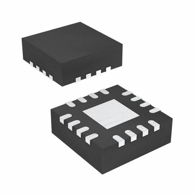
PIN CONFIGURATION
2
(1)
NC = Not connected.
(2)
–VS connected through PowerPAD™.
Submit Documentation Feedback
(1)
OUTA
NC
+VS
OUTB
15
14
13
2
11
-INB
+INA
3
10
+INB
GND
4
9
8
A1
A0
-VS
(2)
7
-INA
6
NC
NC
12
5
1
NC
NC
16
RGV PACKAGE
4×4 QFN-16
(TOP VIEW)
Copyright © 2010, Texas Instruments Incorporated
�OPA2670
www.ti.com
SBOS434 – AUGUST 2010
ELECTRICAL CHARACTERISTICS: VS = +12V
Boldface limits are tested at +25°C. At TA = +25°C, A0 = A1 = 0 (full power), G = +5V/V, RF = 432Ω, and RL = 100Ω, and fully
differential specifications, unless otherwise noted. See Figure 38 for ac performance only.
OPA2670IRGV
PARAMETER
CONDITIONS
MIN
TYP
MAX
UNITS
TEST
LEVEL (1)
AC PERFORMANCE
Small-signal bandwidth
G = +5V/V, RF = 750Ω, VO = 2VPP
420
MHz
C
G=+10V/V, RF = 750Ω, VO = 500mVPP
140
MHz
C
Bandwidth for 0.1dB flatness
G = +5V/V, VO = 2VPP
80
MHz
C
Large-signal bandwidth
G = +5V/V, VO = 10VPP
300
MHz
C
Slew rate (differential)
G = +5V/V, 16V step
5000
V/ms
C
Rise-and-fall time (differential)
G = +5V/V, 2V step
1.3
ns
C
Harmonic distortion
G = +5V/V, VO = 2VPP, 10MHz
2nd harmonic
RL = 100Ω, Diff
–71
dBc
C
3rd harmonic
RL = 100Ω, Diff
–80
dBc
C
Input voltage noise
f > 1MHz, single-ended model
3.6
nV/√Hz
C
Noninverting input current noise
f > 1MHz, single-ended model
6
pA/√Hz
C
Inverting input current noise
f > 1MHz, single-ended model
38
pA/√Hz
C
DC PERFORMANCE (2)
Open-loop transimpedance gain (ZOL)
Input offset voltage
VO = 0V, RL = 100Ω, single-ended amplifier
90
VCM = 0V, single-ended amplifier
150
±2
–40°C to +85°C
kΩ
A
±6
mV
A
±7.2
mV
B
Input offset voltage drift
VCM = 0V, single-ended amplifier
±8
±20
mV/°C
B
Input offset voltage matching
VCM = 0V, single-ended amplifier
±0.5
±4
mV
A
Noninverting input bias current
VCM = 0V, single-ended amplifier
±6
±24
mA
A
±26
mA
B
–40°C to +85°C
Noninverting input bias current drift
VCM = 0V, single-ended amplifier
±9
±40
nA/°C
B
Noninverting Input bias current matching
VCM = 0V, single-ended amplifier
±0.5
±5
mA
A
Inverting input bias current
VCM = 0V, single-ended amplifier
±5
±34
mA
A
±38
mA
B
±62
mA/°C
B
–40°C to +85°C
Inverting input bias current drift
VCM = 0V, single-ended amplifier
±8
INPUT (2)
Common-mode input range
Common-mode rejection ratio
Noninverting input impedance
Inverting input resistance
Each amplifier
±3.5
±3.8
V
A
VCM = 0V, input-referred, single-ended
amplifier
50
56
dB
A
–40°C to +85°C
48
dB
B
1.5 || 1
MΩ || pF
C
60
Ω
B
0.8
V
A
V
A
Each amplifier
Open-loop, each amplifier
Maximum logic 0
A1, A0
Minimum logic 1
A1, A0
16
45
2
Logic input current
A1 = 0V, A0 = 0V, each line
+5
Shutdown isolation
G = +4V/V, f = 1MHz, A1 = A0 = 1
85
(1)
(2)
+10
mA
A
dB
C
Test levels: (A) 100% tested at +25°C. Over temperature limits set by characterization and simulation. (B) Limits set by characterization
and simulation. (C) Typical value only for information.
Current is considered positive-out-of node. VCM is the input common-mode voltage.
Copyright © 2010, Texas Instruments Incorporated
Submit Documentation Feedback
3
�OPA2670
SBOS434 – AUGUST 2010
www.ti.com
ELECTRICAL CHARACTERISTICS: VS = +12V (continued)
Boldface limits are tested at +25°C. At TA = +25°C, A0 = A1 = 0 (full power), G = +5V/V, RF = 432Ω, and RL = 100Ω, and fully
differential specifications, unless otherwise noted. See Figure 38 for ac performance only.
OPA2670IRGV
UNITS
TEST
LEVEL (1)
±5
V
C
±4.8
V
B
±4.7
V
A
±500
±700
mA
A
VO = 0V, A1 = 0, A0 = 1, each amplifier
±500
±600
mA
A
VO = 0V, A1 = 1, A0 = 0, each amplifier
±450
±500
mA
A
VO = 0V, each amplifier
1.2
A
C
Closed-loop output impedance at full bias
G = +4V/V, f ≤ 100kHz, A1 = 0, A0 = 0,
each amplifier
0.01
Ω
C
Closed-loop output impedance at mid bias
G = +4V/V, f ≤ 1MHz, A1 = 0, A0 = 1,
each amplifier
0.01
Ω
C
Closed-loop output impedance at low bias
G = +4V/V, f ≤ 1MHz, A1 = 1, A0 = 0,
each amplifier
0.02
Ω
C
each amplifier
25 || 4
kΩ || pF
C
Inputs at GND, each amplifier
±20
mV
C
+12.6
V
A
+12.6
V
B
31.5
mA
A
32.5
mA
B
24
mA
A
25
mA
B
16
mA
A
17
mA
B
1
mA
A
1.2
mA
B
250
ns
C
54
dB
A
–40 to
+85
°C
C
PowerPAD soldered to PCB
51.2
°C/W
C
PowerPAD floating (3)
75
°C/W
C
PARAMETER
CONDITIONS
MIN
TYP
50Ω differential load, each amplifier
±4.7
20Ω differential load, each amplifier
±4.55
Output current at full bias (peak)
VO = 0V, A1 = 0, A0 = 0, each amplifier
Output current at mid bias (peak)
Output current at low bias (peak)
MAX
OUTPUT
Voltage output swing
No load, each amplifier
Short-circuit current
Output impedance at shutdown
Output switching glitch
POWER SUPPLY
Specified operating voltage
+5.5
+12
–40°C to +85°C
Quiescent current at full bias
Supply current at mid bias
Supply current at low bias
Supply current (disabled)
VS = +12V, A1 = 0, A0 = 0
29.5
–40°C to +85°C
28.5
VS = +12V, A1 = 0, A0 = 1
20
–40°C to +85°C
19
VS = +12V, A1 = 1, A0 = 0
13
–40°C to +85°C
12
VS = +12V, A1 = 1, A0 = 1
30.5
22
14
0.9
–40°C to +85°C
Supply current step time
Time to reach 90% final value
Power-supply rejection ratio
(+PSRR)
Input-referred
48
THERMAL CHARACTERISTICS
Specified operating temperature range
RGV package
Thermal resistance, q JA
RGV
(3)
Junction-to-ambient
QFN-16
PowerPAD is physically connected to the negative supply (–VS) for dual-supply configuration or the ground (GND) for single-supply
configuration.
THERMAL INFORMATION
OPA2670
THERMAL METRIC (1)
RGV
UNITS
16 PINS
qJA
Junction-to-ambient thermal resistance
51.2
qJCtop
Junction-to-case (top) thermal resistance
56.7
qJB
Junction-to-board thermal resistance
54.3
yJT
Junction-to-top characterization parameter
3.5
yJB
Junction-to-board characterization parameter
35.6
qJCbot
Junction-to-case (bottom) thermal resistance
2.5
(1)
4
°C/W
For more information about traditional and new thermal metrics, see the IC Package Thermal Metrics application report, SPRA953.
Submit Documentation Feedback
Copyright © 2010, Texas Instruments Incorporated
�OPA2670
www.ti.com
SBOS434 – AUGUST 2010
TYPICAL CHARACTERISTICS: Full Bias
At TA = +25°C, IQ = 30.5mA, Full Bias, and RL_Differential = 100Ω, unless otherwise noted.
SMALL-SIGNAL FREQUENCY RESPONSE
6
0
3
−3
0
Normalized Gain (dB)
Normalized Gain (dB)
SMALL-SIGNAL FREQUENCY RESPONSE
3
−6
−9
−12
−15
Full Bias
G = +10V/V
RL = 100Ω
VO = 2VPP
−18
−21
1
10
Frequency (MHz)
100
−9
−12
−18
500
Full Bias
G = +5V/V
RL = 100Ω
VO = 2VPP
1
10
100
Frequency (MHz)
800
Figure 1.
Figure 2.
LARGE-SIGNAL FREQUENCY RESPONSE
OUTPUT VOLTAGE AND
OUTPUT CURRENT LIMITATIONS
6
5
0
4
2W Internal
Power Dissipation
Single Channel
3
−3
Output Voltage (V)
Normalized Gain (dB)
−6
−15
3
−6
−9
−12
−15
2
1
0
−1
−2
2W Internal
Power Dissipation
Single Channel
10Ω Load Line
25Ω Load Line
100Ω Load Line
−3
Full Bias
G = +5V/V
RL = 100Ω
VO = 10VPP
−18
−21
−3
50Ω Load Line
−4
−5
1
10
Frequency (MHz)
100
−6
200 400
−1000 −800 −600 −400 −200 0
Output Current (mA)
500
Figure 3.
600
800 1000
Figure 4.
OVERDRIVE RECOVERY
INPUT OFFSET VOLTAGE
4
20
3
Input Voltage
Output Voltage 15
2
10
1
5
0
0
−1
−5
−2
−10
−3
−15
−4
−20
100
600
0
10
20
30
40
50
60
Time (ns)
70
Figure 5.
Copyright © 2010, Texas Instruments Incorporated
80
90
Count (Units)
Output Voltage (V)
Input Voltage (V)
500
400
300
200
100
0
−0.9 −0.3 0.3 0.9 1.5 2.1 2.7 3.3 3.9 4.5 5.1 5.7
Input Offset Voltage (mV)
Figure 6.
Submit Documentation Feedback
5
�OPA2670
SBOS434 – AUGUST 2010
www.ti.com
TYPICAL CHARACTERISTICS: Full Bias (continued)
At TA = +25°C, IQ = 30.5mA, Full Bias, and RL_Differential = 100Ω, unless otherwise noted.
HARMONIC DISTORTION
vs FREQUENCY
HARMONIC DISTORTION
vs LOAD
−35
−35
Harmonic Distortion (dBc)
−45
−55
Second-Order Harmonic Distortion
Third-Order Harmonic Distortion
−65
−75
−85
−95
1
10
Frequency (MHz)
−65
−75
−85
−105
50
Full Bias
f = 5MHz
G = +5V/V
VO = 2VPP
10
100
Figure 7.
Figure 8.
HARMONIC DISTORTION
vs OUTPUT VOLTAGE
HARMONIC DISTORTION
vs SUPPLY VOLTAGE
−84
Full Bias
f = 5MHz
G = +5V/V
RL = 100Ω
Full Bias
f = 5MHz
G = +5V/V
RL = 100Ω
VO = 2VPP
−86
Harmonic Distortion (dBc)
−65
−75
−85
−95
1
−88
−90
−92
−94
Second-Order Harmonic Distortion
Third-Order Harmonic Distortion
−96
10
Second-Order Harmonic Distortion
Third-Order Harmonic Distortion
3
3.5
Output Voltage (VPP)
5.5
HARMONIC DISTORTION
vs BIAS CURRENT
TWO-TONE, THIRD-ORDER
INTERMODULATION INTERCEPT
−85
−90
Second-Order Harmonic Distortion
Third-Order Harmonic Distortion
Mid
Bias Current
Figure 11.
Submit Documentation Feedback
f = 5MHz
G = +5V/V
RL = 100Ω
VO = 2VPP
Low
Third-Order Intermodulation Intercept (dBc)
Harmonic Distortion (dBc)
5
Figure 10.
−80
−100
High
4.5
Figure 9.
−75
−95
4
6
Supply Voltage (±VS)
−70
6
500
Load (Ω)
−55
Harmonic Distortion (dBc)
−55
−95
−105
0.5
−105
Second-Order Harmonic Distortion
Third-Order Harmonic Distortion
−45
Harmonic Distortion (dBc)
Full Bias
G = +5V/V
RL = 100Ω
VO = 2VPP
50
Low Bias
Mid Bias
High Bias
45
40
35
30
25
Measured at 50Ω matched load
20
0
10
20
30
Frequency (MHz)
40
50
Figure 12.
Copyright © 2010, Texas Instruments Incorporated
�OPA2670
www.ti.com
SBOS434 – AUGUST 2010
TYPICAL CHARACTERISTICS: Full Bias (continued)
At TA = +25°C, IQ = 30.5mA, Full Bias, and RL_Differential = 100Ω, unless otherwise noted.
LARGE-SIGNAL
ENABLE/DISABLE RESPONSE
DISABLE FEEDTHROUGH
vs FREQUENCY
6
6
−3
4
−6
−50
−60
Gain (dB)
−70
−80
2
−90
0
−100
−2
0
10
20
Time (ns)
30
40
−110
1
10
Figure 13.
INPUT NOISE DENSITY
140
120
−20
110
−40
100
−60
90
−80
80
−100
70
−120
60
−140
50
−160
10k
100k
1M
Frequency (Hz)
10M
100M
1k
Input Voltage Noise Density
Inverting Input Current Noise Density
Noninverting Input Current Noise Density
Input Voltage Noise Density (nV/rtHz)
0
Phase (°)
Gain
Phase
130
Transimpedance Gain (dBΩ)
1k
20
1k
100
100
10
10
1
100
−180
1G
1k
Figure 15.
50
40
40
30
30
20
20
10
Common-Mode Rejection Ratio
Power-Supply Rejection Ratio
100k
1M
Frequency (Hz)
Figure 17.
Copyright © 2010, Texas Instruments Incorporated
10M
0
100M
Output Impedance (Ω)
50
10k
1
10M
10
Power-Supply Rejection Ratio (dB)
Common-Mode Rejection Ratio (dB)
60
1k
1M
OUTPUT IMPEDANCE
60
0
100
10k
100k
Frequency (Hz)
Figure 16.
COMMON-MODE REJECTION RATIO AND
POWER-SUPPLY REJECTION RATIO
10
1k
Figure 14.
OPEN-LOOP TRANSIMPEDANCE
GAIN AND PHASE
40
100
100
Frequency (MHz)
Input Current Noise Density (pA/rtHz)
Disable Voltage (V)
0
Output Voltage (V)
3
−40
1
0.1
0.01
0.001
100
1k
10k
100k
1M
Frequency (Hz)
10M
100M
Figure 18.
Submit Documentation Feedback
7
�OPA2670
SBOS434 – AUGUST 2010
www.ti.com
TYPICAL CHARACTERISTICS: Full Bias (continued)
At TA = +25°C, IQ = 30.5mA, Full Bias, and RL_Differential = 100Ω, unless otherwise noted.
520
31
510
30.5
500
+ IQ
− IQ
+ IOUT
− IOUT
30
−25
0
25
50
Temperature (°C)
75
100
3
8
2
6
1
4
−25
0
25
50
Temperature (°C)
75
100
Figure 20.
TYPICAL DC DRIFT MATCHING
vs TEMPERATURE
QUIESCENT CURRENT
vs SUPPLY VOLTAGE
0
1
0
−1
−1
−1.5
−2
−2
−3
−2.5
−4
−3
−5
−3.5
−6
−4
−7
Input Offset Voltage (VOS)
Inverting Input Bias Current (− IB)
Noninverting Input Bias Current (+ IB)
−4.5
−5
−25
10
Figure 19.
−0.5
−5.5
−50
12
4
0
−50
480
125
0
25
50
Temperature (°C)
75
100
2
125
35
−8
30
Quiescent Current (mA)
Input Offset Voltage Matching (mV)
29.5
−50
5
490
14
Input Offset Voltage (VOS)
Inverting Input Bias Current (− IB)
Noninverting Input Bias Current (+ IB)
Input Bias Current (µA)
31.5
6
Output Current (mA)
530
Input Offset Voltage (mV)
32
TYPICAL DC DRIFT
vs TEMPERATURE
Input Bias Current Matching (µA)
Quiescent Current (mA)
QUIESCENT CURRENT AND OUTPUT CURRENT
vs TEMPERATURE
−9
25
20
15
+ IQ Low Bias
− IQ Low Bias
+ IQ Mid Bias
− IQ Mid Bias
+ IQ Full Bias
− IQ Full Bias
10
5
0
−10
125
−5
2
3
4
5
6
Supply Voltage (±VS)
Figure 21.
Figure 22.
SERIES RESISTANCE
vs CAPACITIVE LOAD
SMALL-SIGNAL FREQUENCY RESPONSE
vs FREQUENCY
3
1k
Normalized Gain (dB)
Series Resistance (Ω)
0
100
10
−3
−6
−9
VIN
−12
−15
1
1
10
100
Capacitive Load (pF)
Figure 23.
8
Submit Documentation Feedback
1k
RS
−18
1M
10pF
24pF
44pF
94pF
330pF
CL
VOUT
RS
10M
Frequency (Hz)
100M
600M
Figure 24.
Copyright © 2010, Texas Instruments Incorporated
�OPA2670
www.ti.com
SBOS434 – AUGUST 2010
TYPICAL CHARACTERISTICS: Full Bias (continued)
At TA = +25°C, IQ = 30.5mA, Full Bias, and RL_Differential = 100Ω, unless otherwise noted.
PULSE RESPONSE
10
5
4VPP
16VPP
4
6
3
4
2
2
1
0
0
−2
−1
−4
−2
−6
−3
−8
−4
−10
0
10
20
30
40
50
60
Time (ns)
70
80
90
Output Voltage (V)
Output Voltage (V)
8
−5
100
Figure 25.
Copyright © 2010, Texas Instruments Incorporated
Submit Documentation Feedback
9
�OPA2670
SBOS434 – AUGUST 2010
www.ti.com
TYPICAL CHARACTERISTICS: Mid Bias
At TA = +25°C, IQ = 22mA, Mid Bias, and RL_Differential = 100Ω, unless otherwise noted.
3
−3
0
Normalized Gain (dB)
0
−6
−9
−12
−15
Mid Bias
G = +10V/V
RL = 100Ω
VO = 2VPP
−18
−21
Normalized Gain (dB)
SMALL-SIGNAL FREQUENCY RESPONSE
6
1
−9
−12
10
Frequency (MHz)
100
−18
500
HARMONIC DISTORTION
vs FREQUENCY
−3
−6
−9
−12
Mid Bias
G = +5V/V
RL = 100Ω
VO = 10VPP
10
Frequency (MHz)
100
−55
−65
−75
−85
Second-Order Harmonic Distortion
Third-Order Harmonic Distortion
−105
0.5
500
800
Mid Bias
G = +5V/V
RL = 100Ω
VO = 2VPP
−95
1
10
Frequency (MHz)
Figure 28.
Figure 29.
HARMONIC DISTORTION
vs LOAD
HARMONIC DISTORTION
vs OUTPUT VOLTAGE
50
−55
Mid Bias
f = 5MHz
G = +5V/V
VO = 2VPP
−45
−55
−65
−75
−85
−95
Harmonic Distortion (dBc)
−35
−105
10
100
Frequency (MHz)
LARGE-SIGNAL FREQUENCY RESPONSE
−45
1
1
Figure 27.
0
−15
Mid Bias
G = +5V/V
RL = 100Ω
VO = 2VPP
Figure 26.
−35
−21
Harmonic Distortion (dBc)
−6
3
−18
Mid Bias
f = 5MHz
G = +5V/V
RL = 100Ω
−65
−75
−85
−95
Second-Order Harmonic Distortion
Third-Order Harmonic Distortion
10
100
Load (Ω)
Figure 30.
10
−3
−15
Harmonic Distortion (dBc)
Normalized Gain (dB)
SMALL-SIGNAL FREQUENCY RESPONSE
3
Submit Documentation Feedback
Second-Order Harmonic Distortion
Third-Order Harmonic Distortion
500
−105
1
10
Output Voltage (VPP)
Figure 31.
Copyright © 2010, Texas Instruments Incorporated
�OPA2670
www.ti.com
SBOS434 – AUGUST 2010
TYPICAL CHARACTERISTICS: Low Bias
At TA = +25°C, IQ = 14mA, Low Bias, and RL_Differential = 100Ω, unless otherwise noted.
3
−3
0
Normalized Gain (dB)
0
−6
−9
−12
−15
Low Bias
G = +10V/V
RL = 100Ω
VO = 2VPP
−18
−21
Normalized Gain (dB)
SMALL-SIGNAL FREQUENCY RESPONSE
6
1
−6
−9
−12
10
Frequency (MHz)
100
−18
500
HARMONIC DISTORTION
vs FREQUENCY
−45
−3
−6
−9
−12
Low Bias
G = +5V/V
RL = 100Ω
VO = 10VPP
1
10
Frequency (MHz)
100
−55
−65
−75
−85
Second-Order Harmonic Distortion
Third-Order Harmonic Distortion
−105
0.5
500
800
Low Bias
G = +5V/V
RL = 100Ω
VO = 2VPP
−95
1
10
Frequency (MHz)
Figure 34.
Figure 35.
HARMONIC DISTORTION
vs LOAD
HARMONIC DISTORTION
vs OUTPUT VOLTAGE
50
−55
−35
−55
−65
−75
−85
−95
100
Load (Ω)
Figure 36.
Copyright © 2010, Texas Instruments Incorporated
−65
−70
−75
−80
Second-Order Harmonic Distortion
Third-Order Harmonic Distortion
10
Low Bias
f = 5MHz
G = +5V/V
RL = 100Ω
−60
Harmonic Distortion (dBc)
Low Bias
f = 5MHz
G = +5V/V
VO = 2VPP
−45
−105
10
100
Frequency (MHz)
LARGE-SIGNAL FREQUENCY RESPONSE
0
−21
1
Figure 33.
−35
−15
Low Bias
G = +5V/V
RL = 100Ω
VO = 2VPP
Figure 32.
3
−18
Harmonic Distortion (dBc)
−3
−15
Harmonic Distortion (dBc)
Normalized Gain (dB)
SMALL-SIGNAL FREQUENCY RESPONSE
3
500
−85
Second-Order Harmonic Distortion
Third-Order Harmonic Distortion
1
10
Output Voltage (VPP)
Figure 37.
Submit Documentation Feedback
11
�OPA2670
SBOS434 – AUGUST 2010
www.ti.com
APPLICATION INFORMATION
WIDEBAND CURRENT-FEEDBACK
OPERATION
The OPA2670 provides the exceptional ac
performance of a wideband current-feedback op amp
with a highly linear, high-power output stage.
Requiring only 21mA/port quiescent current, the
OPA2670 swings to within 1V of either supply rail on
a 100Ω load and delivers in excess of 700mA at room
temperature. This low-output headroom requirement,
along with supply voltage independent biasing,
provides remarkable +12V supply operation. The
OPA2670 delivers greater than 420MHz bandwidth
driving a 2VPP output into 100Ω on a +12V supply.
Previous boosted output stage amplifiers typically
suffer from very poor crossover distortion as the
output current goes through zero. The OPA2670
achieves a comparable power gain with much better
linearity.
The
primary
advantage
of
a
current-feedback op amp over a voltage-feedback op
amp is that ac performance (bandwidth and
distortion) is relatively independent of signal gain.
Figure 38 shows the dc-coupled, gain of +10V/V, dual
power-supply circuit configuration used as the basis
of the +12V Electrical and Typical Characteristics. For
test purposes, the input impedance is set to 50Ω with
a resistor to ground and the output impedance is set
to 50Ω with a series output resistor. Voltage swings
reported in the Electrical Characteristics are taken
directly at the input and output pins, whereas load
powers (dBm) are defined at a matched 50Ω load.
For the circuit of Figure 38, the total effective load is
100Ω || 750Ω || 750Ω = 78.9Ω.
+12V
1/2
OPA2670
RF
750W
VIN
RG
167W
RF
750W
This approach allows the user to set a source
termination impedance at the input that is
independent of the signal gain. For instance, simple
differential filters may be included in the signal path
right up to the noninverting inputs with no interaction
with the gain setting. The differential signal gain for
the circuit of Figure 38 is:
RF
AD = 1 + 2 ´
RG
(1)
Where AD = differential gain.
Figure 38 shows a value of 167Ω for the AD = +10V/V
design. Because the OPA2670 is a current feedback
(CFB) amplifier, its bandwidth is primarily controlled
with the feedback resistor value; the differential gain,
however, may be adjusted with considerable freedom
using just the RG resistor. In fact, RG may be reduced
by a reactive network that provides a very isolated
shaping to the differential frequency response.
Various combinations of single-supply or ac-coupled
gain can also be delivered using the basic circuit of
Figure 38. Common-mode bias voltages on the two
noninverting inputs pass on to the output with a gain
of +1V/V because an equal dc voltage at each
inverting node creates no current through RG. This
circuit does show a common-mode gain of +1V/V
from input to output. The source connection should
either remove this common-mode signal if undesired
(using an input transformer can provide this function),
or the common-mode voltage at the inputs can be
used to set the output common-mode bias. If the low
common-mode rejection of this circuit is a problem,
the output interface can also be used to reject that
common-mode. For instance, most modern
differential input analog-to-digital converters (ADCs)
reject common-mode signals very well, while a line
driver application through a transformer also
attenuates the common-mode signal through to the
line.
VOUT
RL
1/2
OPA2670
GDIFF = 1 +
2 ´ RF
RG
=
VOUT
VIN
Figure 38. Noninverting Differential I/O Amplifier
12
Submit Documentation Feedback
Copyright © 2010, Texas Instruments Incorporated
�OPA2670
www.ti.com
SBOS434 – AUGUST 2010
DUAL-SUPPLY VDSL DOWNSTREAM
Figure 39 shows an example of a dual-supply VDSL
downstream driver. Both channels of the OPA2670
are configured as a differential gain stage to provide
signal drive to the primary winding of the transformer
(in Figure 39, a step-up transformer with a turns ratio
of 1:n). The main advantage of this configuration is
the cancellation of all even harmonic-distortion
products. Another important advantage for VDSL is
that each amplifier must only swing half of the total
output required driving the load.
LINE DRIVER HEADROOM MODEL
+12V
The first step in a transformer-coupled, twisted-pair
driver design is to compute the peak-to-peak output
voltage from the target specifications. This calculation
is done using the following equations:
VRMS2
PL = 10 ´ log
(1mW) ´ RL
(4)
1/2
OPA2670
IP
RS
RF
1:n
RP
AFE
2VPP
Max
Assumed
The two back-termination resistors (RS) added at
each terminal of the transformer make the impedance
of the modem match the impedance of the phone
line, and also provide a means of detecting the
received signal for the receiver. The value of these
resistors (RS) is a function of the line impedance and
the transformer turns ratio (n), given by the following
equation:
ZLINE
RS =
2n2
(3)
ZLINE
RG
RP
RL
100W
RS
RF
with:
• PL = power at the load
• VRMS = voltage at the load
• RL = load impedance
These values produce the following:
1/2
OPA2670
IP
Figure 39. Dual-Supply VDSL Downstream Driver
The analog front-end (AFE) signal is ac-coupled to
the driver, and the noninverting input of each
amplifier is biased to the mid-supply voltage (ground
in this case). In addition to providing the proper
biasing to the amplifier, this approach also provides a
high-pass filtering with a corner frequency. Because
the signal bandwidth starts at 26kHz, this high-pass
filter does not generate any problem and has the
advantage of filtering out unwanted lower
frequencies.
The input signal is amplified with a gain set by the
following equation:
2 ´ RF
GD = 1 +
RG
(2)
VRMS =
(1mW) ´ RL ´ 10
PL
10
(5)
VP = CrestFactor ´ VRMS = CF ´ VRMS
(6)
with:
• VP = peak voltage at the load
• CF = Crest Factor
VLPP = 2 ´ CF ´ VRMS
(7)
with VLPP = peak-to-peak voltage at the load.
Consolidating Equation 4 through Equation 7 allows
us to express the required peak-to-peak voltage at
the load as a function of the crest factor, the load
impedance, and the power at the load. Thus:
VLPP = 2 ´ CF ´
(1mW) ´ RL ´ 10
PL
10
(8)
VLPP is usually computed for a nominal line
impedance and may be taken as a fixed design
target.
The next step in the design is to compute the
individual amplifier output voltage and currents as a
function of peak-to-peak voltage on the line and
transformer turns ratio.
Copyright © 2010, Texas Instruments Incorporated
Submit Documentation Feedback
13
�OPA2670
SBOS434 – AUGUST 2010
www.ti.com
As this turns ratio changes, the minimum allowed
supply voltage changes along with it. The peak
current in the amplifier output is given by:
2 ´ VLPP
1
1
±IP =
´
´
n
2
4RS
(9)
with VPP as defined in Equation 8, and RM as defined
in Equation 3 and shown in Figure 40.
RS
VPP =
2VLPP
n
VLPP
n
RL
VLPP
V1,V2, R1, and R2 are given in Table 1 for +12V
operation.
Table 1. Line Driver Headroom Model Values
+12V
V1
R1
V2
R2
0.8V
0.3Ω
0.8V
0.6Ω
When using a synthetic output impedance circuit (see
Figure 39), a significant drop is noticed in bandwidth
from the specification that appears in the Electrical
Characteristics table. This apparent drop in
bandwidth for the differential signal is a result of the
apparent increase in the feedback transimpedance as
seen
for
each
amplifier.
This
feedback
transimpedance equation is given below.
RS
1+2´
ZFB = RF ´
RS
1+2´
Figure 40. Driver Peak Output Voltage
With the previous information available, it is now
possible to select a supply voltage and the turns ratio
desired for the transformer, as well as calculate the
headroom for the OPA2670.
RS
+
+
RL
RS
RP
RL
RS
RP
RF
-
RP
(12)
To increase 0.1dB flatness to the frequency of
interest, adding a serial RC in parallel with the gain
resistor may be needed, as shown in Figure 42.
RS
1/2
OPA2670
The model, shown in Figure 41, can be described
with the following set of equations:
1. As the available output swing:
VPP = VCC - (V1 + V2) - IP ´ (R1 + R2)
(10)
RF
RP
RM
2. Or as the required supply voltage:
VCC = VPP + (V1 + V2) + IP ´ (R1 + R2)
ZLINE
(11)
The minimum supply voltage for power and load
requirements is given by Equation 11.
VIN
RG
RP
100W
CM
RF
+VCC
1/2
OPA2670
RS
R1
V1
Figure 42. +0.1dB Flatness Compensation Circuit
VOUT
IP
V2
R2
Figure 41. Line Driver Headroom Model
14
Submit Documentation Feedback
Copyright © 2010, Texas Instruments Incorporated
�OPA2670
www.ti.com
SBOS434 – AUGUST 2010
TOTAL DRIVER POWER FOR xDSL
APPLICATIONS
The total internal power dissipation for the OPA2670
in an xDSL line driver application is the sum of the
quiescent power and the output stage power. The
OPA2670 holds a relatively constant quiescent
current versus supply voltage—giving a power
contribution that is simply the quiescent current times
the supply voltage used. The total output stage power
can be computed with reference to Figure 43.
+VCC
IAVG =
IP
CF
RT
Figure 43. Output Stage Power Model
The two output stages used to drive the load of
Figure 40 can be seen as an H-Bridge in Figure 43.
The average current drawn from the supply into this
H-Bridge and load is the peak current in the load
divided by the crest factor (CF) for the xDSL
modulation. This total power from the supply is then
reduced by the power in RT, leaving the power
dissipated internal to the drivers in the four output
stage transistors. That power is simply the target line
power used in Equation 4 plus the power lost in the
matching elements (RS). In the following examples, a
perfect match is targeted giving the same power in
the matching elements as in the load.
For a target line power of 100mW into 100Ω, the
voltage at the load is 3.16VRMS and the current is
31.6mARMS. Bringing this load current to the amplifier
side and using a 1:2 turns ratio to be 63.2mARMS, the
average current is then:
2
IAVG = 63.2mARMS ? 2 ? p = 56.89mA (average)
(13)
With a +12V power supply, the average driving power
is 683mW.
If the total quiescent current is used to drive the load,
the total average power consumption for Low Bias
mode is then (per port):
2
12V ? 14mA ?
+ 683mW = 750mW
5
(14)
Copyright © 2010, Texas Instruments Incorporated
OUTPUT CURRENT AND VOLTAGE
The OPA2670 provides output voltage and current
capabilities that are unsurpassed in a low-cost, dual
monolithic op amp. The output voltage for a 50Ω
differential load tested at +25°C typically swings
closer than 1.3V to either supply rail. Into a 20Ω load
(the minimum tested load), the amplifier delivers more
than ±450mA continuous and greater than ±1A peak
output current.
The specifications described above, though familiar in
the industry, consider voltage and current limits
separately. In many applications, it is the voltage
times current (or V-I product) that is more relevant to
circuit operation. Refer to the Output Voltage and
Current Limitations plot (Figure 4) in the Typical
Characteristics. The X- and Y-axes of this graph
show the zero-voltage output current limit and the
zero-current output voltage limit, respectively. The
four quadrants give a more detailed view of the
OPA2670 output drive capabilities, noting that the
graph is bounded by a safe operating area of 2W
maximum internal power dissipation (in this case, for
one channel only). Superimposing resistor load lines
onto the plot shows that the OPA2670 can drive
±5.1V into 100Ω or ±5V into 50Ω without exceeding
the output capabilities or the 1W dissipation limit. A
100Ω load line (the standard test circuit load) shows
the full +12V output swing capability, as shown in the
Electrical Characteristics table. The minimum
specified output voltage and current over temperature
are set by worst-case simulations at the cold
temperature extreme. Only at cold startup do the
output current and voltage decrease to the numbers
shown in the Electrical Characteristics table. As the
output transistors deliver power, the junction
temperature increases, decreasing the VBEs
(increasing the available output voltage swing), and
increasing the current gains (increasing the available
output current). In steady-state operation, the
available output voltage and current are always
greater than that shown in the over-temperature
specifications, because the output stage junction
temperatures are higher than the minimum specified
operating ambient temperature. To maintain
maximum output stage linearity, no output
short-circuit protection is provided. This absence of
short-circuit protection is normally not a problem
because most applications include a series-matching
resistor at the output that limits the internal power
dissipation if the output side of this resistor is shorted
to ground. However, shorting the output pin directly to
the adjacent positive power-supply pin, in most
cases, destroys the amplifier. If additional short-circuit
protection is required, a small series resistor may be
included in the supply lines. Under heavy output
loads, this additional resistor reduces the available
output voltage swing. A 5Ω series resistor in each
power-supply lead limits the internal power
dissipation to less than 2W for an output short-circuit,
Submit Documentation Feedback
15
�OPA2670
SBOS434 – AUGUST 2010
www.ti.com
while decreasing the available output voltage swing
only 0.5V for up to 100mA desired load currents.
Always place the 0.1mF power-supply decoupling
capacitors after these supply current limiting resistors,
directly on the supply pins.
connections to multiple devices can easily cause this
value to be exceeded. Always consider this effect
carefully, and add the recommended series resistor
as close as possible to the OPA2670 output pin (see
the Board Layout Guidelines section).
DRIVING CAPACITIVE LOADS
DISTORTION PERFORMANCE
One of the most demanding and yet very common
load conditions for an op amp is capacitive loading.
Often, the capacitive load is the input of an
ADC—including additional external capacitance that
may be recommended to improve the ADC linearity.
A high-speed, high open-loop gain amplifier such as
the OPA2670 can be very susceptible to decreased
stability and closed-loop response peaking when a
capacitive load is placed directly on the output pin.
When the amplifier open-loop output resistance is
considered, this capacitive load introduces an
additional pole in the signal path that can decrease
the phase margin. Several external solutions to this
problem have been suggested.
The OPA2670 provides good distortion performance
into a 100Ω load on +12V supplies. Relative to
alternative
solutions,
the
amplifier
provides
exceptional performance into lighter loads. Generally,
until the fundamental signal reaches very high
frequency or power levels, the second harmonic
dominates the distortion with a negligible
third-harmonic component. Focusing then on the
second harmonic, increasing the load impedance
improves distortion directly. Remember that the total
load includes the feedback network—in the
noninverting, fully-differential configuration (see
Figure 38), this value is the sum of 2RF + RG.
When the primary considerations are frequency
response flatness, pulse response fidelity, and/or
distortion, the simplest and most effective solution is
to isolate the capacitive load from the feedback loop
by inserting a series isolation resistor between the
amplifier output and the capacitive load. This series
resistor does not eliminate the pole from the loop
response, but shifts it and adds a zero at a higher
frequency. The additional zero acts to cancel the
phase lag from the capacitive load pole, thus
increasing the phase margin and improving stability.
The Typical Characteristics show the recommended
RS vs Capacitive Load (see Figure 23 and Figure 24)
and the resulting frequency response at the load.
Parasitic capacitive loads greater than 2pF can begin
to degrade device performance. Long printed circuit
board (PCB) traces, unmatched cables, and
16
Submit Documentation Feedback
In most op amps, increasing the output voltage swing
directly increases harmonic distortion. The Typical
Characteristics show the second harmonic increasing
at a little less than the expected 2x rate, whereas the
third harmonic increases at a little less than the
expected 3x rate. Where the test power doubles, the
difference between it and the second harmonic
decreases less than the expected 6dB, whereas the
difference between it and the third harmonic
decreases by less than the expected 12dB. This
difference also shows up in the two-tone, third-order
intermodulation spurious (IM3) response curves. The
third-order spurious levels are extremely low at
low-output power levels. The output stage continues
to hold them low even as the fundamental power
reaches very high levels.
Copyright © 2010, Texas Instruments Incorporated
�OPA2670
www.ti.com
SBOS434 – AUGUST 2010
DIFFERENTIAL NOISE PERFORMANCE
The OPA2670 is designed to be used as a differential
driver in xDSL applications. Therefore, it is important
to analyze the noise in such a configuration.
Figure 44 shows the op amp noise model for the
differential configuration.
Dividing this expression by the differential noise gain
[GD = (1 + 2RF/RG)] gives the equivalent
input-referred spot noise voltage at the noninverting
input, as shown in Equation 17.
EO =
2
iIRF
2
2 ´ eN + (iN ´ RS) + 4kTRS + 2
2
+2
4kTRF
GD
GD
(17)
IN
Evaluating these equations for the OPA2670 ADSL
circuit and component values of Figure 39 gives a
total output spot noise voltage of 66.7nV/√Hz and a
total equivalent input spot noise voltage of
6.67nV/√Hz
EN
RS
IN
ERS
RF
In order to minimize the output noise as a result of
the noninverting input bias current noise, it is
recommended to keep the noninverting source
impedance as low as possible.
4kTRF
4kTRS
RG
2
EO
4kTRG
RF
4kTRF
IN
EN
RS
IN
ERS
4kTRS
Figure 44. Differential Op Amp Noise Analysis
Model
As a reminder, the differential gain is expressed as:
2 ´ RF
GD = 1 +
RG
(15)
The output noise can be expressed as shown below:
EO =
2
2
A current-feedback op amp such as the OPA2670
provides exceptional bandwidth in high gains, giving
fast pulse settling but only moderate dc accuracy.
The Electrical Characteristics show an input offset
voltage comparable to high-speed, voltage-feedback
amplifiers; however, the two input bias currents are
somewhat higher and are unmatched. While bias
current cancellation techniques are very effective with
most voltage-feedback op amps, they do not
generally reduce the output dc offset for wideband
current-feedback op amps. Because the two input
bias currents are unrelated in both magnitude and
polarity, matching the input source impedance to
reduce error contribution to the output is ineffective.
Evaluating the configuration of Figure 38, using a
worst-case condition at +25°C input offset voltage
and the two input bias currents, gives a worst-case
output offset range equal to:
VOFF = ±(NG × VOS(MAX)) + (IBN × RS/2 × NG)
±(IBI × RF)
where NG = noninverting signal gain
=
±(10 × 6mV)
±(750Ω × 34mA)
+
(24mA
×
25Ω
×
10)
2
2 ´ GD2 ´ eN + (iN ´ RS) + 4kTRS + 2(iIRF) + 2(4kTRFGD)
(16)
Copyright © 2010, Texas Instruments Incorporated
DC ACCURACY AND OFFSET CONTROL
= ±60mV ± 6mV ± 25.5mV
VOFF = ±121.8mV
Submit Documentation Feedback
17
�OPA2670
SBOS434 – AUGUST 2010
BOARD LAYOUT GUIDELINES
Achieving
optimum
performance
with
a
high-frequency amplifier such as the OPA2670
requires careful attention to board layout parasitic and
external component types. Recommendations that
optimize performance include:
a) Minimize parasitic capacitance to any ac ground
for all of the signal I/O pins. Parasitic capacitance on
the output and inverting input pins can cause
instability; on the noninverting input, it can react with
the source impedance to cause unintentional band
limiting. To reduce unwanted capacitance, a window
around the signal I/O pins should be opened in all of
the ground and power planes around those pins.
Otherwise, ground and power planes should be
unbroken elsewhere on the board. .
b) Minimize the distance (less than 0.25in, or
6,35mm)
from
the
power-supply
pins
to
high-frequency 0.1mF decoupling capacitors. At the
device pins, the ground and power plane layout
should not be in close proximity to the signal I/O pins.
Avoid narrow power and ground traces to minimize
inductance between the pins and the decoupling
capacitors. The power-supply connections should
always be decoupled with these capacitors. An
optional supply decoupling capacitor across the two
power supplies (for bipolar operation) improves
second-harmonic distortion performance. Larger
(2.2mF to 6.8mF) decoupling capacitors, effective at
lower frequencies, should also be used on the main
supply pins. These capacitors can be placed
somewhat farther from the device and may be shared
among several devices in the same area of the PCB.
c) Careful selection and placement of external
components
preserve
the
high-frequency
performance of the OPA2670. Resistors should be
a very low reactance type. Surface-mount resistors
work best and allow a tighter overall layout. Metal film
and carbon composition, axially-leaded resistors can
also provide good high-frequency performance.
Again, keep leads and PCB trace length as short as
possible. Never use wire-wound type resistors in a
high-frequency application. Although the output pin
and inverting input pin are the most sensitive to
parasitic capacitance, always position the feedback
and series output resistor, if any, as close as possible
to the output pin. Other network components, such as
noninverting input termination resistors, should also
be placed close to the package. Where double-side
component mounting is allowed, place the feedback
resistor directly under the package on the other side
of the board between the output and inverting input
pins. The frequency response is primarily determined
by the feedback resistor value as described
previously. Increasing the value reduces the
18
Submit Documentation Feedback
www.ti.com
bandwidth, whereas decreasing it leads to a more
peaked frequency response. The 750Ω feedback
resistor used in the Typical Characteristics at a gain
of +10V/V on +12V supplies is a good starting point
for design.
d) Connections to other wideband devices on the
board may be made with short direct traces or
through onboard transmission lines. For short
connections, consider the trace and the input to the
next device as a lumped capacitive load. Relatively
wide traces (50mils to 100mils [.050in to .100in, or
1,27mm to 2,54mm]) should be used, preferably with
ground and power planes opened up around them.
Estimate the total capacitive load and set RS from the
plot of RS vs Capacitive Load (see Figure 23 and
Figure 24). Low parasitic capacitive loads (less than
5pF) may not need an isolation resistor because the
OPA2670 is nominally compensated to operate with a
2pF parasitic load. If a long trace is required, and the
6dB signal loss intrinsic to a doubly-terminated
transmission line is acceptable, implement a
matched-impedance
transmission
line
using
microstrip or stripline techniques (consult an ECL
design handbook for microstrip and stripline layout
techniques). A 50Ω environment is not necessary on
board; in fact, a higher impedance environment
improves distortion (see the distortion versus load
plots). With a characteristic board trace impedance
defined based on board material and trace
dimensions, a matching series resistor into the trace
from the output of the OPA2670 is used, as well as a
terminating shunt resistor at the input of the
destination device. Remember also that the
terminating impedance is the parallel combination of
the shunt resistor and the input impedance of the
destination device.
This total effective impedance should be set to match
the trace impedance. The high output voltage and
current capability of the OPA2670 allows multiple
destination devices to be handled as separate
transmission lines, each with their own series and
shunt terminations. If the 6dB attenuation of a
doubly-terminated transmission line is unacceptable,
a long trace can be series-terminated at the source
end only.
Treat the trace as a capacitive load in this case and
set the series resistor value as shown in the plot of
RS vs Capacitive Load. However, this configuration
does not preserve signal integrity as well as a
doubly-terminated line. If the input impedance of the
destination device is low, there is some signal
attenuation as a result of the voltage divider formed
by the series output into the terminating impedance.
Copyright © 2010, Texas Instruments Incorporated
�OPA2670
www.ti.com
e) Socketing a high-speed part such as the
OPA2670 is not recommended. The additional lead
length and pin-to-pin capacitance introduced by the
socket can create an extremely troublesome parasitic
network, which can make it almost impossible to
achieve a smooth, stable frequency response. Best
results are obtained by soldering the OPA2670
directly onto the board.
Copyright © 2010, Texas Instruments Incorporated
SBOS434 – AUGUST 2010
f) Use the –VS plane to conduct heat out of the
QFN-16 PowerPAD package. This package attaches
the die directly to an exposed thermal pad on the
bottom, which should be soldered to the board. This
pad must be connected electrically to the same
voltage plane as the most negative supply applied to
the OPA2670 (in Figure 39, this supply is GND).
Submit Documentation Feedback
19
�PACKAGE MATERIALS INFORMATION
www.ti.com
3-Jun-2022
TAPE AND REEL INFORMATION
REEL DIMENSIONS
TAPE DIMENSIONS
K0
P1
B0 W
Reel
Diameter
Cavity
A0
B0
K0
W
P1
A0
Dimension designed to accommodate the component width
Dimension designed to accommodate the component length
Dimension designed to accommodate the component thickness
Overall width of the carrier tape
Pitch between successive cavity centers
Reel Width (W1)
QUADRANT ASSIGNMENTS FOR PIN 1 ORIENTATION IN TAPE
Sprocket Holes
Q1
Q2
Q1
Q2
Q3
Q4
Q3
Q4
User Direction of Feed
Pocket Quadrants
*All dimensions are nominal
Device
Package Package Pins
Type Drawing
SPQ
Reel
Reel
A0
Diameter Width (mm)
(mm) W1 (mm)
B0
(mm)
K0
(mm)
P1
(mm)
W
Pin1
(mm) Quadrant
OPA2670IRGVR
VQFN
RGV
16
2500
330.0
12.4
4.25
4.25
1.15
8.0
12.0
Q2
OPA2670IRGVT
VQFN
RGV
16
250
180.0
12.4
4.25
4.25
1.15
8.0
12.0
Q2
Pack Materials-Page 1
�PACKAGE MATERIALS INFORMATION
www.ti.com
3-Jun-2022
TAPE AND REEL BOX DIMENSIONS
Width (mm)
W
L
H
*All dimensions are nominal
Device
Package Type
Package Drawing
Pins
SPQ
Length (mm)
Width (mm)
Height (mm)
OPA2670IRGVR
VQFN
RGV
16
2500
356.0
356.0
35.0
OPA2670IRGVT
VQFN
RGV
16
250
210.0
185.0
35.0
Pack Materials-Page 2
�GENERIC PACKAGE VIEW
RGV 16
VQFN - 1 mm max height
PLASTIC QUAD FLATPACK - NO LEAD
4 x 4, 0.65 mm pitch
Images above are just a representation of the package family, actual package may vary.
Refer to the product data sheet for package details.
4224748/A
www.ti.com
�PACKAGE OUTLINE
RGV0016A
VQFN - 1 mm max height
SCALE 3.000
PLASTIC QUAD FLATPACK - NO LEAD
4.15
3.85
B
A
PIN 1 INDEX AREA
4.15
3.85
C
1.0
0.8
SEATING PLANE
0.08 C
0.05
0.00
2.16 0.1
2X 1.95
SYMM
(0.2) TYP
8
5
(0.37) TYP
EXPOSED
THERMAL PAD
9
4
2X 1.95
SYMM
17
2.16 0.1
12X 0.65
1
12
PIN 1 ID
13
16
16X
0.65
0.45
16X
0.38
0.23
0.1
0.05
C A B
4219037/A 06/2019
NOTES:
1. All linear dimensions are in millimeters. Any dimensions in parenthesis are for reference only. Dimensioning and tolerancing
per ASME Y14.5M.
2. This drawing is subject to change without notice.
3. The package thermal pad must be soldered to the printed circuit board for thermal and mechanical performance.
www.ti.com
�EXAMPLE BOARD LAYOUT
RGV0016A
VQFN - 1 mm max height
PLASTIC QUAD FLATPACK - NO LEAD
( 2.16)
SYMM
SEE SOLDER MASK
DETAIL
13
16
16X (0.75)
16X (0.305)
12
1
17
SYMM
12X (0.65)
(3.65)
(0.83)
4
9
(R0.05) TYP
( 0.2) TYP
VIA
5
8
(0.83)
(3.65)
LAND PATTERN EXAMPLE
EXPOSED METAL SHOWN
SCALE: 20X
0.07 MIN
ALL AROUND
0.07 MAX
ALL AROUND
METAL UNDER
SOLDER MASK
METAL EDGE
EXPOSED METAL
SOLDER MASK
OPENING
EXPOSED
METAL
NON SOLDER MASK
DEFINED
(PREFERRED)
SOLDER MASK
OPENING
SOLDER MASK DEFINED
SOLDER MASK DETAILS
4219037/A 06/2019
NOTES: (continued)
4. This package is designed to be soldered to a thermal pad on the board. For more information, see Texas Instruments literature
number SLUA271 (www.ti.com/lit/slua271).
5. Vias are optional depending on application, refer to device data sheet. If any vias are implemented, refer to their locations shown
on this view. It is recommended that vias under paste be filled, plugged or tented.
www.ti.com
�EXAMPLE STENCIL DESIGN
RGV0016A
VQFN - 1 mm max height
PLASTIC QUAD FLATPACK - NO LEAD
(0.58) TYP
16
13
16X (0.75)
16X (0.305)
1
12
(0.58) TYP
17
SYMM
12X (0.65)
(3.65)
4X (0.96)
4
9
(R0.05) TYP
8
5
4X (0.96)
SYMM
(3.65)
SOLDER PASTE EXAMPLE
BASED ON 0.125 MM THICK STENCIL
SCALE: 20X
EXPOSED PAD 17
79% PRINTED SOLDER COVERAGE BY AREA UNDER PACKAGE
4219037/A 06/2019
NOTES: (continued)
6. Laser cutting apertures with trapezoidal walls and rounded corners may offer better paste release. IPC-7525 may have alternate
design recommendations.
www.ti.com
�IMPORTANT NOTICE AND DISCLAIMER
TI PROVIDES TECHNICAL AND RELIABILITY DATA (INCLUDING DATA SHEETS), DESIGN RESOURCES (INCLUDING REFERENCE
DESIGNS), APPLICATION OR OTHER DESIGN ADVICE, WEB TOOLS, SAFETY INFORMATION, AND OTHER RESOURCES “AS IS”
AND WITH ALL FAULTS, AND DISCLAIMS ALL WARRANTIES, EXPRESS AND IMPLIED, INCLUDING WITHOUT LIMITATION ANY
IMPLIED WARRANTIES OF MERCHANTABILITY, FITNESS FOR A PARTICULAR PURPOSE OR NON-INFRINGEMENT OF THIRD
PARTY INTELLECTUAL PROPERTY RIGHTS.
These resources are intended for skilled developers designing with TI products. You are solely responsible for (1) selecting the appropriate
TI products for your application, (2) designing, validating and testing your application, and (3) ensuring your application meets applicable
standards, and any other safety, security, regulatory or other requirements.
These resources are subject to change without notice. TI grants you permission to use these resources only for development of an
application that uses the TI products described in the resource. Other reproduction and display of these resources is prohibited. No license
is granted to any other TI intellectual property right or to any third party intellectual property right. TI disclaims responsibility for, and you
will fully indemnify TI and its representatives against, any claims, damages, costs, losses, and liabilities arising out of your use of these
resources.
TI’s products are provided subject to TI’s Terms of Sale or other applicable terms available either on ti.com or provided in conjunction with
such TI products. TI’s provision of these resources does not expand or otherwise alter TI’s applicable warranties or warranty disclaimers for
TI products.
TI objects to and rejects any additional or different terms you may have proposed. IMPORTANT NOTICE
Mailing Address: Texas Instruments, Post Office Box 655303, Dallas, Texas 75265
Copyright © 2022, Texas Instruments Incorporated
�


 工商网监
湘ICP备2023018690号
工商网监
湘ICP备2023018690号
