OPA512
®
Very-High Current—High Power
OPERATIONAL AMPLIFIER
FEATURES
APPLICATIONS
● WIDE SUPPLY RANGE: ±10V to ±50V
● HIGH OUTPUT CURRENT: 15A Peak
● CLASS A/B OUTPUT STAGE:
Low Distortion
●
●
●
●
●
● VOLTAGE-CURRENT LIMIT PROTECTION
CIRCUIT
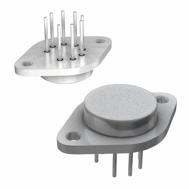
● SMALL TO-3 PACKAGE
DESCRIPTION
The OPA512 is a high voltage, very-high current
operational amplifier designed to drive a wide variety
of resistive and reactive loads. Its complementary
class A/B output stage provides superior performance
in applications requiring freedom from cross-over
distortion. User-set current limit circuitry provides
protection to the amplifier and load in fault conditions.
A resistor-programmable voltage-current limiter
circuit may be used to further protect the amplifier
from damaging conditions.
3
SERVO AMPLIFIER
MOTOR DRIVER
SYNCRO EXCITATION
AUDIO AMPLIFIER
TEST PIN DRIVER
The OPA512 employs a laser-trimmed monolithic
integrated circuit to bias the output transistors, providing excellent low-level signal fidelity and high output
voltage swing. The reduced internal parts count made
possible with this monolithic IC improves performance and reliability.
This hybrid integrated circuit is housed in a hermetic
TO-3 package and all circuitry is electrically-isolated
from the case. This allows direct mounting to a chassis
or heat sink without cumbersome insulating hardware
and provides optimum heat transfer.
+VS
2
4
5
RCL+
1
Bias
Circuit
Out
7
RCL–
8
RVI
(Optional)
6
–VS
International Airport Industrial Park • Mailing Address: PO Box 11400
Tel: (520) 746-1111 • Twx: 910-952-1111 • Cable: BBRCORP •
©
1985 Burr-Brown Corporation
SBOS144
• Tucson, AZ 85734 • Street Address: 6730 S. Tucson Blvd. • Tucson, AZ 85706
Telex: 066-6491 • FAX: (520) 889-1510 • Immediate Product Info: (800) 548-6132
PDS-600B
Printed in U.S.A. December, 1993
�SPECIFICATIONS
ELECTRICAL
At TC = +25°C, and VS = ±40V, unless otherwise noted.
OPA512BM
PARAMETER
CONDITIONS
INPUT OFFSET VOLTAGE
Initial Offset
vs Temperature
vs Supply Voltage
vs Power
INPUT BIAS CURRENT
Initial
vs Temperature
vs Supply Voltage
INPUT OFFSET CURRENT
Initial
vs Temperature
MIN
Specified Temp. Range
Specified Temp. Range
Specfied Temp. Range
INPUT IMPEDANCE, DC
INPUT CAPACITANCE
VOLTAGE RANGE
Common-Mode Voltage
Common-Mode Rejection
GAIN
Open-Loop Gain at 10Hz
Gain-Bandwidth Product, 1MHz
Power Bandwidth
Phase Margin
OUTPUT
Voltage Swing (1)
Specified Temp. Range
Specified Temp. Range
1kΩ Load
Specified Temp. Range
8Ω Load
8Ω Load
8Ω Load
Specified Temp. Range
8Ω Load
BM at 10A, SM at 15A
Specified Temp. Range
IO = 80mA
IO = 5A
Current, Peak
Settling Time to 0.1%
Slew Rate
Capacitive Load
POWER SUPPLY
Voltage
Current, Quiescent
THERMAL RESISTANCE
AC Junction-to-Case(3)
DC Junction-to-Case
Junction to Air
TEMPERATURE RANGE
Specified
±(|VS| – 5)
74
MAX
TYP
MAX
UNITS
±2
±10
±30
±20
±6
±65
±200
±1
*
*
*
±3
±40
*
mV
µV/°C
µV/V
µV/V
12
±50
±10
30
400
10
*
*
20
*
nA
pA/°C
pA/V
±12
±50
±30
±5
*
±10
nA
pA/°C
*
MΩ
3
*
pF
*
*
V
dB
*
dB
*
*
*
dB
MHz
kHz
*
Degrees
*
*
110
96
108
4
20
13
*
*
20
±(|VS| – 6)
±(|VS| – 7)
V
±(|VS| – 5)
±(|VS| – 5)
10
*
*
15
V
V
A
µs
V/µs
2
4
2.5
Specified Temp. Range
G=1
Specified Temp. Range
G > 10
±10
TC = –55°C to +125°C,
f > 60Hz
TC = –55°C to +125°C
TC = –55°C to +125°C
TC
MIN
200
±(|VS| – 3)
100
2V Step
Specified Temp. Range
OPA512SM
TYP
–25
*
*
*
1.5
*
SOA(2)
*
±40
25
±45
50
0.8
1.25
30
0.9
1.4
+85
*
–55
nF
*
*
±50
35
V
mA
*
*
*
*
*
°C/W
°C/W
°C/W
+125
°C
*Specification same as OPA512BM.
NOTES: (1) +VS and –VS denote the postive and negative supply voltage, respectively. Total VS is measured from +VS to –VS. (2) SOA = Safe Operating Area.
(3) Rating applies if the output current alternates between both output transistors at a rate faster than 60Hz.
The information provided herein is believed to be reliable; however, BURR-BROWN assumes no responsibility for inaccuracies or omissions. BURR-BROWN assumes
no responsibility for the use of this information, and all use of such information shall be entirely at the user’s own risk. Prices and specifications are subject to change
without notice. No patent rights or licenses to any of the circuits described herein are implied or granted to any third party. BURR-BROWN does not authorize or warrant
any BURR-BROWN product for use in life support devices and/or systems.
®
OPA512
2
�ABSOLUTE MAXIMUM RATINGS
CONNECTION DIAGRAM
Supply Voltage, +VS to –VS ................................................................ 100V
Output Current: Source ........................................................................ 15A
Sink .................................................................... see SOA
Power Dissipation, Internal(1) ............................................................ 125W
Input Voltage: Differential ........................................................ ±(|VS| – 3V)
Common-mode ............................................................. ±VS
Temperature: Pins (soldering, 10s) ................................................ +300°C
Junction(1) ............................................................... +200°C
Temperature Range: Storage(2) ...................................... –65°C to +150°C
Operating (Case) .......................... –55°C to +125°C
Top View
+RCL
+Current
Limit
+VS
3
2
+In 4
1
–In 5
8
Output
–RCL
NOTES: (1) Long term operation at the maximum junction temperature will
result in reduced product life. Derate internal power dissipation to achieve
high MTTF. (2) OPA512BM, –55°C to +100°C.
6
–VS
7
RVI
–Current
Limit
ORDERING INFORMATION
MODEL
PACKAGE
TEMPERATURE RANGE
OPA512BM
OPA512SM
8-pin TO-3
8-pin TO-3
–25°C to +85°C
–55°C to +125°C
PACKAGE INFORMATION
MODEL
PACKAGE
PACKAGE DRAWING
NUMBER(1)
OPA512BM
OPA512SM
8-Pin TO-3
8-Pin TO-3
030
030
NOTE: (1) For detailed drawing and dimension table, please see end of data
sheet, or Appendix D of Burr-Brown IC Data Book.
®
3
OPA512
�TYPICAL PERFORMANCE CURVES
TA = 25°C, VS = ±40VDC, unless otherwise noted.
BIAS CURRENT
2.5
120
2.2
Normalized Bias Current, IB
Internal Power Dissipation, P (W)
POWER DERATING
140
100
80
60
40
BM
SM
20
0
1.9
1.6
1.3
1.0
0.7
0.4
0
20
40
60
80
100
120
140
–50
–25
Case Temperature, TC (°C)
15.0
100
VO = 0
RCL = 0.06Ω, RVI = ∞
10.0
7.5
VO = 24V
5.0
RCL = 0.18Ω, RVI = 0
VO = 0
25
50
75
100
125
1M
10M
SMALL SIGNAL RESPONSE
120
Open-Loop Gain, A (dB)
Current Limit, ILIM (A)
CURRENT LIMIT
17.5
12.5
0
Case Temperature, TC (°C)
2.5
80
60
40
20
0
VO = –24V
0
–20
–50
–25
0
25
50
75
100
125
1
10
100
1k
Case Temperature, TC (°C)
PHASE RESPONSE
100k
POWER RESPONSE
0
100
–30
68
Output Voltage, VO (Vp-p)
Phase, φ (degrees)
10k
Frequency, f (Hz)
–60
–90
–120
–150
–180
|+VS| + |–VS| = 100V
|+VS| + |–VS| = 80V
46
32
22
|+VS| + |–VS| = 30V
15
10
6.8
–210
4.6
1
10
100
1k
10k
100k
1M
10M
10
Frequency, f (Hz)
30
Frequency, f (kHz)
®
OPA512
20
4
50
70
100
�TYPICAL PERFORMANCE CURVES (CONT)
TA = 25°C, VS = ±40VDC, unless otherwise noted.
PULSE RESPONSE
COMMON-MODE REJECTION
8
VIN = ±5V, tR = 100ns
6
100
Output Voltage, VO (V)
Common-Mode Rejection, CMR (dB)
120
80
60
40
20
4
2
0
–2
–4
–6
–8
0
1
10
100
1k
10k
100k
0
1M
2
4
8
12
10
HARMONIC DISTORTION
100
3
70
1
50
Distortion (%)
Input Noise Voltage, VN (nV/√Hz)
INPUT NOISE
40
30
20
G = 10
VS = ±37V
RL = 4Ω
0.3
PO = 4W
PO = 100mW
0.1
0.03
PO = 120W
0.01
0.003
10
0
100
1k
100
100k
10k
300
1k
3k
10k
30k
100k
Frequency, f (Hz)
Frequency, f (Hz)
QUIESCENT CURRENT
OUTPUT VOLTAGE SWING
1.6
Voltage Drop From Supply (V)
6
1.4
Normalized, IQ
6
Time, t (µs)
Frequency, f (Hz)
TC = –25°C
1.2
TC = +25°C
1.0
TC = +85°C
0.8
TC = +125°C
0.6
0.4
5
4
–VO
3
+VO
2
1
40
50
60
70
80
90
100
0
Total Supply Voltage, VS (V)
3
6
9
12
15
Output Current, IO (A)
®
5
OPA512
�APPLICATIONS INFORMATION
POWER SUPPLIES
15
Output Current (A)
Specifications for the OPA512 are based on a nominal
operating voltage of ±40V. A single power supply or unbalanced supplies may be used as long as the maximum total
operating voltage (total of +VS and –VS) is not greater than
90V (100V for OPA512SM model.)
CURRENT LIMITS
Current limit resistors must be provided for proper operation. Independent positive and negative current limit values
may be selected by choice of RCL+ and RCL–, respectively.
Resistor values are calculated by:
Thermal Limit
t = 5ms
t = 1ms
10
8
6
5
4
3
t = 0.5ms
TC = +125°C
TC = +25°C
2
1.5
TC = +85°C
1
0.8
0.5
0.4
0.3
0.2
Secondary Breakdown
5
6 7 8 9 10
15
20
40
60
80 100
Voltage Across Output Transistor (V)
RCL = 0.65/ILIM (amps) –0.007
FIGURE 1. Safe Operating Area.
This is the nominal current limit value at room temperature.
The maximum output current decreases at high temperature
as shown in the typical performance curve. Most wirewound resistors are satisfactory, but some highly inductive
types may cause loop stability problems. Be sure to evaluate
performance with the actual resistors to be used in production.
under normal load conditions. Sensing both the output current and the output voltage, this limiter circuit increases the
current limit value as the output voltage approaches the
power supply voltage (where power dissipation is low.) This
type of limiting is achieved by connecting pin 7 through a
programming resistor to ground. The V-I limiter circuit is
governed by the equation:
HEAT SINKING
Power amplifiers are rated by case temperature (not ambient
temperature.) The maximum allowable power dissipation is
a function of the case temperature as shown in the power
derating curve. Load characteristics, signal conditions, and
power supply voltage determine the power dissipated by the
amplifier. The case temperature will be determined by the
heat sinking conditions. Sufficient heat sinking must be
provided to keep the case temperature within safe bounds
given the power dissipated and ambient temperature. See
Application Bulletin AB-038 for further details.
0.65 +
ILIMIT =
0.28 VO
20 + RVI
RCL + 0.007
where:
ILIMIT is the maximum current available at a given output
voltage.
RVI is the value (kΩ) of the resistor from pin 7 to ground.
RCL is the current limit resistor in ohms.
VO is the instantaneous output voltage in volts.
SAFE OPERATING AREA (SOA)
Reactive or EMF-generating loads may produce unusual
(perhaps undesirable) waveforms with the V-I limit circuit
driven into limit. Since current peaks in a reactive load do
not align with the output voltage peaks, the output waveform
will not appear as a simple voltage-limited waveform.
Response of the load to the limiter, in fact, may produce a
“backfire” reaction producing unusual output waveforms.
The safe area plot provides a comprehensive summary of the
power handling limitations of a power amplifier, including
maximum current, voltage and power as well as the secondary breakdown region (see Figure 1) It shows the allowable
output current as a function of the power supply to output
voltage differential (voltage across the conducting power
device.) See Application Bulletin AB-039 for details on
SOA.
VOLTAGE-CURRENT LIMITER CIRCUITRY
The voltage-current (V-I) limiter circuit provides a means to
protect the amplifier from SOA damage such as a short
circuit to ground, yet allows high output currents to flow
®
OPA512
6
�PACKAGE OPTION ADDENDUM
www.ti.com
3-Oct-2003
PACKAGING INFORMATION
ORDERABLE DEVICE
STATUS(1)
PACKAGE TYPE
PACKAGE DRAWING
PINS
PACKAGE QTY
OPA512BM
NRND
TO/SOT
LMF
8
18
OPA512SM
NRND
TO/SOT
LMF
8
18
(1) The marketing status values are defined as follows:
ACTIVE: Product device recommended for new designs.
LIFEBUY: TI has announced that the device will be discontinued, and a lifetime-buy period is in effect.
NRND: Not recommended for new designs. Device is in production to support existing customers, but TI does not recommend using this part in
a new design.
PREVIEW: Device has been announced but is not in production. Samples may or may not be available.
OBSOLETE: TI has discontinued the production of the device.
�IMPORTANT NOTICE
Texas Instruments Incorporated and its subsidiaries (TI) reserve the right to make corrections, modifications,
enhancements, improvements, and other changes to its products and services at any time and to discontinue
any product or service without notice. Customers should obtain the latest relevant information before placing
orders and should verify that such information is current and complete. All products are sold subject to TI’s terms
and conditions of sale supplied at the time of order acknowledgment.
TI warrants performance of its hardware products to the specifications applicable at the time of sale in
accordance with TI’s standard warranty. Testing and other quality control techniques are used to the extent TI
deems necessary to support this warranty. Except where mandated by government requirements, testing of all
parameters of each product is not necessarily performed.
TI assumes no liability for applications assistance or customer product design. Customers are responsible for
their products and applications using TI components. To minimize the risks associated with customer products
and applications, customers should provide adequate design and operating safeguards.
TI does not warrant or represent that any license, either express or implied, is granted under any TI patent right,
copyright, mask work right, or other TI intellectual property right relating to any combination, machine, or process
in which TI products or services are used. Information published by TI regarding third-party products or services
does not constitute a license from TI to use such products or services or a warranty or endorsement thereof.
Use of such information may require a license from a third party under the patents or other intellectual property
of the third party, or a license from TI under the patents or other intellectual property of TI.
Reproduction of information in TI data books or data sheets is permissible only if reproduction is without
alteration and is accompanied by all associated warranties, conditions, limitations, and notices. Reproduction
of this information with alteration is an unfair and deceptive business practice. TI is not responsible or liable for
such altered documentation.
Resale of TI products or services with statements different from or beyond the parameters stated by TI for that
product or service voids all express and any implied warranties for the associated TI product or service and
is an unfair and deceptive business practice. TI is not responsible or liable for any such statements.
Following are URLs where you can obtain information on other Texas Instruments products and application
solutions:
Products
Amplifiers
Applications
amplifier.ti.com
Audio
www.ti.com/audio
Data Converters
dataconverter.ti.com
Automotive
www.ti.com/automotive
DSP
dsp.ti.com
Broadband
www.ti.com/broadband
Interface
interface.ti.com
Digital Control
www.ti.com/digitalcontrol
Logic
logic.ti.com
Military
www.ti.com/military
Power Mgmt
power.ti.com
Optical Networking
www.ti.com/opticalnetwork
Microcontrollers
microcontroller.ti.com
Security
www.ti.com/security
Telephony
www.ti.com/telephony
Video & Imaging
www.ti.com/video
Wireless
www.ti.com/wireless
Mailing Address:
Texas Instruments
Post Office Box 655303 Dallas, Texas 75265
Copyright 2003, Texas Instruments Incorporated
�