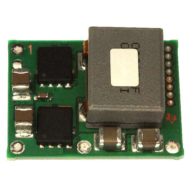
PTD08A020W
www.ti.com
SLTS286F – MAY 2007 – REVISED FEBRUARY 2010
20-A, 4.75-V to 14-V INPUT, NON-ISOLATED,
WIDE-OUTPUT, DIGITAL POWERTRAIN™ MODULE
Check for Samples: PTD08A020W
FEATURES
APPLICATIONS
•
•
•
•
1
2
•
•
•
•
•
Up to 20-A Output Current
4.75-V to 14-V Input Voltage
Programmable Wide-Output Voltage
(0.7 V to 3.6 V)
Efficiencies up to 96%
Digital I/O
– PWM signal
– INHIBIT
– Current limit flag (FAULT)
– Sychronous Rectifier Enable (SRE)
Analog I/O
– Temperature
– Output currrent
Safety Agency Approvals: (Pending)
– UL/IEC/CSA-C22.2 60950-1
Operating Temperature: –40°C to 85°C
Digital Power Systems
using UCD92XX Digital Controllers
DESCRIPTION
The PTD08A020W is a high-performance 20-A rated, non-isolated digital PowerTrain module. This module is the
power conversion section of a digital power system which incorporates TI's UCD7230 MOSFET driver IC. The
PTD08A020W must be used in conjunction with a digital power controller such as the UCD9240 or UCD9110
family. The PTD08A020W receives control signals from the digital controller and provides parametric and status
information back to the digital controller. Together, PowerTrain modules and a digital power controller form a
sophisticated, robust, and easily configured power management solution.
Operating from an input voltage range of 4.75 V to 14 V, the PTD08A020W provides step-down power
conversion to a wide range of output voltages from, 0.7 V to 3.6 V. The wide input voltage range makes the
PTD08A020W particularly suitable for advanced computing and server applications that utilize a loosely
regulated 8-V, 9.6-V or 12-V intermediate distribution bus. Additionally, the wide input voltage range increases
design flexibility by supporting operation with tightly regulated 5-V or 12-V intermediate bus architectures.
The module incorporates output over-current and temperature monitoring which protects against most load faults.
Output current and module temperature signals are provided for the digital controller to permit user defined
over-current and over-temperature warning and fault scerarios.
The module uses double-sided surface mount construction to provide a low profile and compact footprint.
Package options include both through-hole and surface mount configurations that are lead (Pb) - free and RoHS
compatible.
1
2
Please be aware that an important notice concerning availability, standard warranty, and use in critical applications of Texas
Instruments semiconductor products and disclaimers thereto appears at the end of this data sheet.
POWERTRAIN is a trademark of Texas Instruments.
PRODUCTION DATA information is current as of publication date.
Products conform to specifications per the terms of the Texas
Instruments standard warranty. Production processing does not
necessarily include testing of all parameters.
Copyright © 2007–2010, Texas Instruments Incorporated
�PTD08A020W
SLTS286F – MAY 2007 – REVISED FEBRUARY 2010
www.ti.com
This integrated circuit can be damaged by ESD. Texas Instruments recommends that all integrated circuits be handled with
appropriate precautions. Failure to observe proper handling and installation procedures can cause damage.
ESD damage can range from subtle performance degradation to complete device failure. Precision integrated circuits may be more
susceptible to damage because very small parametric changes could cause the device not to meet its published specifications.
Standard PTD08A020W Application
Digital Lines
To/From
Digital Controller
12
11
VBIAS PWM
10
9
SRE FAULT
8
INH
VO
VI
1
VO
VI
4
PTD08A020W
+
CI1
CI2
330 mF
22 mF
(Recommended) (Optional)
L
O
A
D
+
GND
TEMP
2
5
IOUT AGND
6
7
GND
3
GND
CO1
47 mF
(Optional)
CO2
330 mF
(Recommended)
GND
Analog Lines To
Digital Controller
UDG-07054
2
Submit Documentation Feedback
Copyright © 2007–2010, Texas Instruments Incorporated
Product Folder Link(s): PTD08A020W
�PTD08A020W
www.ti.com
SLTS286F – MAY 2007 – REVISED FEBRUARY 2010
ORDERING INFORMATION
For the most current package and ordering information, see the Package Option Addendum at the end of this datasheet, or see
the TI website at www.ti.com.
DATASHEET TABLE OF CONTENTS
DATASHEET SECTION
PAGE NUMBER
ENVIRONMENTAL AND ABSOLUTE MAXIMUM RATINGS
3
ELECTRICAL CHARACTERISTICS TABLE
4
TERMINAL FUNCTIONS
5
TYPICAL CHARACTERISTICS (VI = 12V)
6
TYPICAL CHARACTERISTICS (VI = 5V)
8
TYPICAL APPLICATION SCHEMATIC
10
GRAPHICAL USER INTERFACE VALUES
11
TRAY DRAWINGS
12
ENVIRONMENTAL AND ABSOLUTE MAXIMUM RATINGS
(Voltages are with respect to GND)
UNIT
VI
Input voltage
VB
Bias voltage
TA
Operating temperature range Over VI range
Twave
Wave soldering temperature
Surface temperature of module body or pins for 5
seconds maximum.
Tstg
Storage temperature
Storage temperature of module removed from shipping package
Tpkg
Packaging temperature
Shipping Tray or Tape and Reel storage or bake temperature
45
Mechanical shock
Per Mil-STD-883D, Method 2002.3, 1 msec, 1/2
sine, mounted
250
Mechanical vibration
Mil-STD-883D, Method 2007.2, 20-2000 Hz
V
16
V
–40 to 85
suffix AD
suffix AD
260
Reliability
Per Telcordia SR-332, 50% stress, TA = 40°C, ground benign
Flammability
Meets UL94V-O
Product Folder Link(s): PTD08A020W
G
7.4
grams
9.26
106 Hr
Submit Documentation Feedback
Copyright © 2007–2010, Texas Instruments Incorporated
°C
–55 to 125
15
Weight
MTBF
16
3
�PTD08A020W
SLTS286F – MAY 2007 – REVISED FEBRUARY 2010
www.ti.com
ELECTRICAL CHARACTERISTICS
PTD08A020W
TA= 25°C, FSW= 350kHz, VI= 12 V, VO= 3.3 V, VB= VI, CI1= 330 µF, CI2= 22 µF ceramic, CO1= 47 µF ceramic, CO2= 330 µF,
and IO= IO(max) (unless otherwise stated)
PARAMETER
TEST CONDITIONS
PTD08A010W
MIN
UNIT
MAX
IO
Output current
Over VO range
0
20
A
VI
Input voltage range
Over IO range
4.75
14 (1)
V
VOADJ
Output voltage adjust range
Over IO range
0.7 (1)
3.6
V
Efficiency
h
VOPP
VO Ripple (peak-to-peak)
VB
Bias voltage
VB
UVLO
Bias voltage under voltage
lockout
IB
Bias current
VIH
High-level input voltage
VIL
Low-level input voltage
PWM input
TEMP output
25°C, natural convection
TYP
IO = 20 A,
fs = 350 kHz
VO = 3.3 V
91%
VO = 2.5 V
89%
VO = 1.8 V
86%
VO = 1.5 V
84%
VO = 1.2 V
83%
VO = 1.0 V
80%
20-MHz bandwidth
20
4.75
VB increasing
4.25
4.5
4.75
VB decreasing
4.0
4.25
4.5
Inhibit (pin 8) to AGND
Standby
5
Switching
42
2.0
SRE, INH, & PWM input levels
Frequency range
300
Pulse width limits
130
Range
-40
Accuracy, -40°C ≤ TA ≤ 85°C
-4.0
VOL
FAULT output
ILIM
2.7
Output Impedance
CO
External output capacitance
Equivalent series resistance (non-ceramic)
(1)
(2)
(3)
(4)
(5)
4
125
°C
mV
3.3
0.6
A
V
mV/A
66
86
0.44
0.6
0.76
10
15
20
Nonceramic
330
(2)
Ceramic
22
(2)
Nonceramic
330
(3)
10,000 (4)
47
(3)
(3)
1 (5)
V
3.5
46
Ceramic
°C
500
35
Offset
Capacitance Value
kHz
mV/°C
0.15
External input capacitance
500
+6.0
Overcurrent threshold; Reset, followed by auto-recovery
IOUT output
V
10
0
Gain
V
ns
Low-level output voltage, IFAULT = 4mA
Range
CI
5.5
Slope
High-level output voltage, IFAULT = 4mA
V
mA
0.8
Offset, TA = 0°C
VOH
mVPP
14
V
kΩ
µF
µF
mΩ
The maximum input voltage is duty cycle limited to (VO/(130ns × FSW)) or 14 V, whichever is less. The maximum allowable input voltage
is a function of switching frequency.
A 22 µF ceramic input capacitor is recommended for operation. An additional 330 µF bulk capacitor rated for a minimum of 500mA rms
of ripple current is recommended. Refer to the UCD9240 controller datasheet and user interface for application specific capacitor
specifications.
A 47 µF ceramic output capacitor is recommended for operation. An additional 330 µF bulk capacitor is recommended for improved
transient response. See the related Application Information section for further guidance. Refer to the UCD9240 controller datasheet and
user interface for application specific capacitor specifications.
10,000 µF is the calculated maximum output capacitance given a 1V/msec output voltage rise time. Additional capacitance or increasing
the output voltage rise rate may trigger the overcurrent threshold at start-up.
This is the minimum ESR for all non-ceramic output capacitance. Refer to the UCD9240 controller datasheet and user interface for
application specific capacitor specifications.
Submit Documentation Feedback
Copyright © 2007–2010, Texas Instruments Incorporated
Product Folder Link(s): PTD08A020W
�PTD08A020W
www.ti.com
SLTS286F – MAY 2007 – REVISED FEBRUARY 2010
TERMINAL FUNCTIONS
TERMINAL
NAME
VI
NO.
1
GND
2
3
DESCRIPTION
The positive input voltage power node to the module, which is referenced to common GND.
This is the common ground connection for the VI and VO power connections.
VO
4
The regulated positive power output with respect to GND.
TEMP
5
Temperature sense output. The voltage level on this pin represents the temperature of the module.
IOUT
6
Current sense output. The voltage level on this pin represents the average output current of the module.
AGND
7
Analog ground return. It is the 0 Vdc reference for the control inputs.
INH (1)
8
The inhibit pin is a negative logic input that is referenced to AGND. Applying a low-level signal to this pin disables the
module and turns off the output voltage. A 10 kΩ pull-up to 3.3 V or 5 V is required if the INH signal is not used.
FAULT
9
Current limit flag. The Fault signal is a 3.3 V digital output which is latched high after an over-current condition. The
Fault is reset after two complete PWM cycles without an over-current condition (third rising edge of the PWM).
SRE
10
Synchronized Rectifier Enable. This pin is a high impedance digital input. A 3.3 V or 5 V logic level signals is used to
enable the synchronous rectifier switch. When this signal is high, the module will source and sink output current. When
this signal is low, the module will only source current.
PWM
11
This is the PWM input pin. It is a high impedance digital input that accepts 3.3 V or 5 V logic level signals up to 500
MHz.
VBIAS
12
Bias voltage supply required to power internal circuitry. For optimal performance connect VBIAS to VI.
(1)
Denotes negative logic: Open = Normal operation, Ground = Function active
1
12
11
10
9
8
7
6
5
Texas
Instruments
PTD08A020W
(Top View)
2
3
4
Submit Documentation Feedback
Copyright © 2007–2010, Texas Instruments Incorporated
Product Folder Link(s): PTD08A020W
5
�PTD08A020W
SLTS286F – MAY 2007 – REVISED FEBRUARY 2010
www.ti.com
TYPICAL CHARACTERISTICS (1)
(2)
CHARACTERISTIC DATA (VI = 12 V)
EFFICIENCY vs
LOAD CURRENT
EFFICIENCY vs
LOAD CURRENT
100
6
100
3.3 V
3.3 V
90
80
80
70
0.8 V
1.2 V
1.8 V
60
fSW = 350 kHz
2.5 V
VO (V)
3.3V
2.5V
1.8V
1.2V
0.8V
50
40
1.8 V
5
70
0.8 V
1.2 V
60
1.8 V
fSW = 500 kHz
2.5 V
VO (V)
3.3V
2.5V
1.8V
1.2V
0.8V
50
40
30
PD – Power Dissipation – W
90
h – Efficiency – %
h – Efficiency – %
POWER DISSIPATION vs
LOAD CURRENT
4
8
12
IO – Output Current – A
16
20
3.3 V
1.2 V
3
2.5 V
fSW = 350 kHz
2
VO (V)
3.3V
2.5V
1.8V
1.2V
0.8V
0.8 V
1
30
0
4
0
0
4
8
12
IO – Output Current – A
16
20
0
4
8
12
IO – Output Current – A
16
Figure 1.
Figure 2.
Figure 3.
POWER DISSIPATION vs
LOAD CURRENT
INPUT BIAS CURRENT vs
SWITCHING FREQUENCY
AMBIENT TEMPERATURE vs
LOAD CURRENT
7
100
90
90
80
20
400
IBIAS – Input Bias Current – mA
PD – Power Dissipation – W
6
1.2 V
5
1.8 V
4
1.2 V
3
fSW = 500 kHz
2
0.8 V
1
VO (V)
3.3V
2.5V
1.8V
1.2V
0.8V
4
8
12
16
IO – Output Current – A
Figure 4.
(1)
(2)
6
80
70
60
50
20
30
300
70
60
200
100
50
VO = 1.2 V
fSW = 350 kHz
40
400 LFM
200 LFM
100 LFM
Natural Convection
30
40
0
0
TA – Ambient Temperature – °C
3.3 V
Natural
Convection
20
325
350 375 400 425 450 475
fSW – Switching Frequency – kHz
Figure 5.
500
0
4
8
12
16
IO – Output Current – A
20
Figure 6. Safe Operating Area
The electrical characteristic data has been developed from actual products tested at 25°C. This data is considered typical for the
converter. Applies to Figure 1 thru Figure 5.
The temperature derating curves represent the conditions at which internal components are at or below the manufacturer's maximum
operating temperatures. Derating limits apply to modules soldered directly to a 100 mm x 100 mm double-sided PCB with 2 oz. copper.
Please refer to the mechanical specification for more information. Applies to Figure 6 thru Figure 9.
Submit Documentation Feedback
Copyright © 2007–2010, Texas Instruments Incorporated
Product Folder Link(s): PTD08A020W
�PTD08A020W
www.ti.com
SLTS286F – MAY 2007 – REVISED FEBRUARY 2010
TYPICAL CHARACTERISTICS (3)
AMBIENT TEMPERATURE vs
LOAD CURRENT
(4)
90
AMBIENT TEMPERATURE vs
LOAD CURRENT
90
90
400
400
400
70
60
200
100
50
VO = 1.2 V
fSW = 500 kHz
40
400 LFM
200 LFM
100 LFM
Natural Convection
30
Natural
Convection
80
70
200
60
100
50
VO = 3.3 V
fSW = 350 kHz
40
400 LFM
200 LFM
100 LFM
Natural Convection
30
20
TA – Ambient Temperature – °C
80
TA – Ambient Temperature – °C
80
TA – Ambient Temperature – °C
(continued)
AMBIENT TEMPERATURE vs
LOAD CURRENT
Natural
Convection
4
8
12
16
IO – Output Current – A
20
Figure 7. Safe Operating Area
60
200
50
VO = 3.3 V
fSW = 500 kHz
40
400 LFM
200 LFM
100 LFM
Natural Convection
30
20
0
70
100
Natural
Convection
20
0
4
8
12
16
IO – Output Current – A
Figure 8. Safe Operating Area
20
0
4
8
12
16
IO – Output Current – A
Figure 9. Safe Operating Area
Submit Documentation Feedback
Copyright © 2007–2010, Texas Instruments Incorporated
Product Folder Link(s): PTD08A020W
20
7
�PTD08A020W
SLTS286F – MAY 2007 – REVISED FEBRUARY 2010
www.ti.com
TYPICAL CHARACTERISTICS (1)
(2)
CHARACTERISTIC DATA (VI = 5 V)
EFFICIENCY vs
LOAD CURRENT
POWER DISSIPATION
vs
LOAD CURRENT
EFFICIENCY vs
LOAD CURRENT
6
100
100
1.8 V
0.8 V
1.2 V
2.5 V
fSW = 350 kHz
VO (V)
3.3V
2.5V
1.8V
1.2V
0.8V
4
8
12
IO – Output Current – A
16
fSW = 500 kHz
VO (V)
3.3V
2.5V
1.8V
1.2V
0.8V
2
0.8 V
1
4
8
12
IO – Output Current – A
16
20
0
8
12
IO – Output Current – A
16
Figure 12.
POWER DISSIPATION vs
LOAD CURRENT
INPUT BIAS CURRENT vs
SWITCHING FREQUENCY
AMBIENT TEMPERATURE vs
LOAD CURRENT
90
400
3.3 V
2.5 V
0.8 V
2
1
30
TA – Ambient Temperature – °C
1.2 V
IBIAS – Input Bias Current – mA
1.8 V
3
25
20
15
70
60
200
100
50
VO = 1.2 V
fSW = 350 kHz
40
400 LFM
200 LFM
100 LFM
Natural Convection
30
0
4
20
80
VO (V)
3.3V
2.5V
1.8V
1.2V
0.8V
0
4
Figure 11.
35
4
1.2 V
3
Figure 10.
fSW = 500 kHz
5
4
2.5 V
0
0
20
6
PD – Power Dissipation – W
0.8 V
1.2 V
2.5 V
50
0
8
12
16
IO – Output Current – A
Figure 13.
8
1.8 V
70
60
50
(2)
80
1.8 V
VO (V)
3.3V
2.5V
1.8V
1.2V
0.8V
5
PD – Power Dissipation – W
h – Efficiency – %
h – Efficiency – %
80
60
(1)
fSW = 350 kHz
90
90
70
3.3 V
3.3 V
3.3 V
20
10
300
Natural
Convection
20
325
350 375 400 425 450 475
fSW – Switching Frequency – kHz
Figure 14.
500
0
4
8
12
16
IO – Output Current – A
20
Figure 15. Safe Operating Area
The electrical characteristic data has been developed from actual products tested at 25°C. This data is considered typical for the
converter. Applies to Figure 10 thru Figure 14.
The temperature derating curves represent the conditions at which internal components are at or below the manufacturer's maximum
operating temperatures. Derating limits apply to modules soldered directly to a 100 mm x 100 mm double-sided PCB with 2 oz. copper.
Please refer to the mechanical specification for more information. Applies to Figure 15 thru Figure 18.
Submit Documentation Feedback
Copyright © 2007–2010, Texas Instruments Incorporated
Product Folder Link(s): PTD08A020W
�PTD08A020W
www.ti.com
SLTS286F – MAY 2007 – REVISED FEBRUARY 2010
TYPICAL CHARACTERISTICS (3)
AMBIENT TEMPERATURE vs
LOAD CURRENT
(4)
90
AMBIENT TEMPERATURE vs
LOAD CURRENT
90
90
400
400
400
70
60
200
50
100
VO = 1.2 V
fSW = 500 kHz
40
400 LFM
200 LFM
100 LFM
Natural Convection
30
Natural
Convection
80
70
200
60
100
50
VO = 3.3 V
fSW = 350 kHz
40
400 LFM
200 LFM
100 LFM
Natural Convection
30
20
TA – Ambient Temperature – °C
80
TA – Ambient Temperature – °C
80
TA – Ambient Temperature – °C
(continued)
AMBIENT TEMPERATURE vs
LOAD CURRENT
Natural
Convection
4
8
12
16
IO – Output Current – A
20
Figure 16. Safe Operating Area
60
200
100
50
VO = 3.3 V
fSW = 500 kHz
40
400 LFM
200 LFM
100 LFM
Natural Convection
30
20
0
70
Natural
Convection
20
0
4
8
12
16
IO – Output Current – A
Figure 17. Safe Operating Area
20
0
4
8
12
16
IO – Output Current – A
Figure 18. Safe Operating Area
Submit Documentation Feedback
Copyright © 2007–2010, Texas Instruments Incorporated
Product Folder Link(s): PTD08A020W
20
9
�PTD08A020W
SLTS286F – MAY 2007 – REVISED FEBRUARY 2010
www.ti.com
APPLICATION INFORMATION
DIgital Power
VIN
0.1 mF
10 kW
82.5 kW
VIN
VBIAS
+3.3 V
FCX491A
FAULT
UCD7230 Driver
TEMP
+3.3 V
PWM
4.7 mF
Temp-rail1A
PTD08A020W
Temp Sensor
Commutation
VO
SRE
Logic
0.1 mF
INH
[A]
–Vsens-rail2
+Vsens-rail3
–Vsens-rail3
+Vsens-rail4
–Vsens-rail4
55
56
CS-rail3A
CS-rail4A
CS-rail1B
CS-rail2B
7
44
45
47
BPCap
DPWM-1B
DPWM-2B
DPWM-3A
EAn3
DPWM-4A
EAp4
57
FAULT-1A
EAn4
FAULT-1B
AddrSens0
FAULT-2A
AddrSens1
59
FAULT-2B
CS-1A(COMP1)
3
FAULT-3A
CS-2A(COMP2)
2
FAULT-4A
CS-3A(COMP3)
1
SRE-1A
CS-4A(COMP4)
63
UCD9240RGC
CS-1B
62
SRE-1B
SRE-2A
CS-2B
4
SRE-2B
Vin/Iin
5
SRE-3A
Vtrack
6
SRE-4A
Temp
15
TMUX-0
PMBus-Clk
16
TMUX-1
PMBus-Data
27
TMUX-2
PMBus-Alert
28
39
PMBus-Ctrl
FAN-PWM
PowerGood (TMS)
FAN-TACH
10 kW
SYNC-IN
16
Temp-rail1A
Temp-rail1B
Temp-rail2A
Temp-rail2B
Temp-rail3A
Temp-rail4A
13
14
15
12
1
5
2
4
Dgnd-3
Dgnd-1
Dgnd-2
43
26
Agnd-3
8
Agnd-2
64
49
RESET
48
9
Agnd-1
SYNC-OUT
+3.3 V 10 kW
IOUT
GND
DPWM-1A
DPWM-2A
EAp3
60
CS-rail2A
INH
CS-rail1A
EAn2
54
61
CS-rail1A
46
EAp2
53
V33DIO-2
EAn1
52
V33DIO-1
EAp1
51
V33A
–Vsens-rail1
+Vsens-rail2
50
V33FB
+Vsens-rail1
V33D
52
15 kW
TRST
RCR
17
VIN
Temp-rail1B
18
19
FAULT
20
VBIAS
PTD08A020W
SRE
23
INH
A1
A2
A3
A4
A5
Com
S2
S1
S0
EN
GND
11
12
+Vsens-rail1
–Vsens-rail1
CS-rail1B
13
VIN
14
25
Temp-rail2A
34
FAULT
22
PWM
24
SRE
33
INH
VBIAS
VIN
TEMP
PTD08A010W
GND
35
CS-rail2A
29
VIN
Temp-rail2B
30
FAULT
31
36
38
37
TEMP
INH
FAN-PWM
VIN
PTD08A010W
SRE
42
41
VBIAS
PWM
32
GND
CS-rail2B
+Vsens-rail2
–Vsens-rail2
FAN-Tach
VIN
SyncIn
SyncOut
Temp-rail3A
40
10
10 kW
FAULT
VBIAS
VIN
TEMP
PWM
PTD08A010W
SRE
6
A6
VOUT
GND
IOUT
+Vsens-rail3
–Vsens-rail3
VIN
Temp-rail4A
8
11
VOUT
IOUT
3
10
VOUT
IOUT
CS-rail3A
A0
VOUT
IOUT
INH
+3.3 V
VIN
TEMP
PWM
21
FAULT
VBIAS
PTD08A010W
SRE
INH
A7
CD74HC4051
VIN
TEMP
PWM
CS-rail4A
VOUT
GND
IOUT
+Vsens-rail4
–Vsens-rail4
UDG-08035
Figure 19. Typical Application Schematic
Figure 19 shows the UCD9240 power supply controller working in a system which requires the regulation of four
independent power supplies. The loop for each power supply is created by the respective voltage outputs feeding
into the Error ADC differential inputs, and completed by DPWM outputs feeding into the UCD7230 drivers which
are shown on the PTD08A010W and PTD08A020W modules.
10
Submit Documentation Feedback
Copyright © 2007–2010, Texas Instruments Incorporated
Product Folder Link(s): PTD08A020W
�PTD08A020W
www.ti.com
SLTS286F – MAY 2007 – REVISED FEBRUARY 2010
UCD9240 Graphical User Interface (GUI)
When using the UCD9240 digital controller along with digital PowerTrain modules to design a digital power
system, several internal parameters of the modules are required to run the Fusion Digital Power Designer GUI.
See the plant parameters below for the PTD08A010W and PTD08A020W digital PowerTrain modules.
Table 1. PTD08A010W Plant Parameters
PTD08A010W Plant Parameters
L (µH)
DCR (mΩ)
Rds-on-hi (mΩ)
Rds-on-lo (mΩ)
0.90
2.2
3.6
3.6
Table 2. PTD08A020W Plant Parameters
PTD08A020W Plant Parameters
L (µH)
DCR (mΩ)
Rds-on-hi (mΩ)
Rds-on-lo (mΩ)
1.0
1.5
5.0
2.5
Internal output capacitance is present on the digital PowerTrain modules themselves. When using the GUI
interface this capacitance information must be included along with any additional external capacitance. See the
capacitor parameters below for the PTD08A010W and PTD08A020W digital PowerTrain modules.
Table 3. PTD08A010W Capacitor Parameters
PTD08A010W Capacitor Parameters
C (µF)
ESR (mΩ)
ESL (nH)
Quantity
47
1.5
2.5
1
Table 4. PTD08A020W Capacitor Parameters
PTD08A020W Capacitor Parameters
C (µF)
ESR (mΩ)
ESL (nH)
Quantity
47
1.5
2.5
2
Submit Documentation Feedback
Copyright © 2007–2010, Texas Instruments Incorporated
Product Folder Link(s): PTD08A020W
11
�PTD08A020W
SLTS286F – MAY 2007 – REVISED FEBRUARY 2010
www.ti.com
TRAY
12
Submit Documentation Feedback
Copyright © 2007–2010, Texas Instruments Incorporated
Product Folder Link(s): PTD08A020W
�PACKAGE OPTION ADDENDUM
www.ti.com
16-Jul-2020
PACKAGING INFORMATION
Orderable Device
Status
(1)
Package Type Package Pins Package
Drawing
Qty
Eco Plan
(2)
Lead finish/
Ball material
MSL Peak Temp
Op Temp (°C)
(3)
Device Marking
(4/5)
(6)
PTD08A020WAD
ACTIVE
ThroughHole Module
EGP
12
42
RoHS (In
Work) & Green
(In Work)
SN
Level-1-235C-UNLIM/
Level-3-260C-168HRS
-40 to 85
(1)
The marketing status values are defined as follows:
ACTIVE: Product device recommended for new designs.
LIFEBUY: TI has announced that the device will be discontinued, and a lifetime-buy period is in effect.
NRND: Not recommended for new designs. Device is in production to support existing customers, but TI does not recommend using this part in a new design.
PREVIEW: Device has been announced but is not in production. Samples may or may not be available.
OBSOLETE: TI has discontinued the production of the device.
(2)
RoHS: TI defines "RoHS" to mean semiconductor products that are compliant with the current EU RoHS requirements for all 10 RoHS substances, including the requirement that RoHS substance
do not exceed 0.1% by weight in homogeneous materials. Where designed to be soldered at high temperatures, "RoHS" products are suitable for use in specified lead-free processes. TI may
reference these types of products as "Pb-Free".
RoHS Exempt: TI defines "RoHS Exempt" to mean products that contain lead but are compliant with EU RoHS pursuant to a specific EU RoHS exemption.
Green: TI defines "Green" to mean the content of Chlorine (Cl) and Bromine (Br) based flame retardants meet JS709B low halogen requirements of


 工商网监
湘ICP备2023018690号
工商网监
湘ICP备2023018690号
