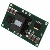
PTH12020W/L
www.ti.com ............................................................................................................................................................. SLTS208I – MAY 2003 – REVISED MARCH 2009
18-A, 12-V INPUT NON-ISOLATED WIDE-OUTPUT
ADJUST POWER MODULE
FEATURES
APPLICATIONS
• Up to 18 A Output Current
• 12-V Input Voltage
• Wide-Output Voltage Adjust
(1.2 V to 5.5 V/(0.8 V to 1.8 V)
• Efficiencies up to 95%
• 195 W/in3 Power Density
• On/Off Inhibit
• Output Voltage Sense
• Pre-Bias Startup
• Under-Voltage Lockout
• Auto-Track™ Sequencing
• Margin Up/Down Controls
• Output Over-Current Protection
(Non-Latching, Auto-Reset)
• Over-Temperature Protection
• Operating Temperature: –40°C to 85°C
• Point-of-Load Alliance (POLA™) Compatible
• Safety Agency Approvals:
UL/IEC/CSA-22.2 60950-1
•
1
2
Complex multi-voltage, multi-processor
systems
NOMINAL SIZE =
1.5 in x 0.87 in
(38,1 mm x 22,1 mm)
DESCRIPTION
The PTH12020 series of non-isolated power modules offers OEM designers a combination of high performance,
small footprint, and industry leading features. As part of a new class of power modules, these products provide
designers with the flexibility to power the most complex multi-processor digital systems using off-the-shelf catalog
parts.
The series employs double-sided surface mount construction and provides highperformance step-down power
conversion for up to 18A of output current from a 12-V input bus voltage. The output voltage of the W-suffix parts
can be set to any value over the range, 1.2V to 5.5V. The L-suffix parts have an adjustment range of 0.8V to
1.8V. The output voltage is set using a single resistor.
This series includes Auto-Track™ sequencing. Auto-Track sequencing simplifies the task of supply voltage
sequencing in a power system by enabling modules to track each other, or any external voltage, during power up
and power down. Other operating features include an on/off inhibit, output voltage adjust (trim), margin up/down
controls, and the ability to start up into an existing output voltage or prebias. For improved load regulation, an
output voltage sense is provided. A non-latching over-current trip and overtemperature shutdown feature protects
against load faults.
Target applications include complex multivoltage, multiprocessor systems that incorporate the industry's
high-speed DSPs, microprocessors and bus drivers.
For start-up into a non-prebiased output, review page 14 in the Application Information section.
For start-up into a prebiased output, review page 18 in the Application Information section.
1
2
Please be aware that an important notice concerning availability, standard warranty, and use in critical applications of Texas
Instruments semiconductor products and disclaimers thereto appears at the end of this data sheet.
POLA, TMS320 are trademarks of Texas Instruments.
PRODUCTION DATA information is current as of publication date.
Products conform to specifications per the terms of the Texas
Instruments standard warranty. Production processing does not
necessarily include testing of all parameters.
Copyright © 2003–2009, Texas Instruments Incorporated
�PTH12020W/L
SLTS208I – MAY 2003 – REVISED MARCH 2009 ............................................................................................................................................................. www.ti.com
These devices have limited built-in ESD protection. The leads should be shorted together or the device placed in conductive foam
during storage or handling to prevent electrostatic damage to the MOS gates.
STANDARD APPLICATION
Track
Margin Down
Margin Up
10 9 8
1
2
VIN
7
PTH12020x
(T o p V i ew)
3 4 5
VO Sense
Inhibit
+
RSET
CIN
560 mF
(Required)
VOUT
6
+ C
OUT
330 mF
(Optional)
L
O
A
D
GND
GND
ORDERING INFORMATION
For the most current package and ordering information, see the Package Option Addendum at the end of this datasheet, or see
the TI website at www.ti.com
ABSOLUTE MAXIMUM RATINGS
over operating free-air temperature range unless otherwise noted
(1)
UNIT
Vtrack
Track input
–0.3V to VI +0.3 V
TA
Operating temperature
range
Over VI Range
Twave
Wave solder temperature
Surface temperature of module body or pins
(5 seconds maximum)
Treflow
Solder reflow temperature
Surface temperature of module body or pins
Tstg
Storage temperature
Storage temperature of module removed from shipping package
Tpkg
Packaging temperature
Shipping Tray or Tape and Reel storage or bake temperature
45°C
Mechanical shock
Per Mil-STD-883D, Method 2002.3 1 msec, 1/2 Sine, mounted
500 G
Mechanical vibration
Mil-STD-883D, Method 2007.2 20-2000 Hz
20 G
Weight
Flammability
(1)
(2)
2
–40C to 85C
PTH12020WAH
260°C
(2)
PTH12020WAS
235°C
(2)
PTH12020WAZ
260°C
(2)
PTH12020WAD
–55°C to 125°C
7 grams
Meets UL 94V-O
Stresses beyond those listed under absolute maximum ratings may cause permanent damage to the device. These are stress ratings
only, and functional operation of the device at these or any other conditions beyond those indicated under recommended operating
conditions is not implied. Exposure to absolute-maximum-rated conditions for extended periods may affect device reliability.
During soldering of package version, do not elevate peak temperature of the module, pins or internal components above the stated
maximum.
Submit Documentation Feedback
Copyright © 2003–2009, Texas Instruments Incorporated
Product Folder Link(s) :PTH12020W/L
�PTH12020W/L
www.ti.com ............................................................................................................................................................. SLTS208I – MAY 2003 – REVISED MARCH 2009
ELECTRICAL CHARACTERISTICS
TA = 25°C, VI =12 V, VO = 3.3 V, CI = 560 µF, CO = 0 µF, and Io = Iomax (unless otherwise noted)
PARAMETER
PTH12020W
TEST CONDITIONS
MIN
TYP
MAX
60C, 200 LFM airflow
0
18 (1)
25C, natural convection
0
18 (1)
UNIT
IO
Output current
VI
Input voltage range
Votol
Set-point voltage tolerance
ΔRegtemp
Temperature variation
–40°C 2.5 V
1
%Vo
Recovery time
Vo over/undershoot
–8
8.8
Over VI and Io ranges
CI
External input capacitance
(7)
(8)
mV
Reliability
(3)
mA
1
V/ms
10.4
9.2
0.5
0.24
260
0
Ceramic
0
Per Bellcore TR-332, 50% stress, TA = 40°C, ground benign
V
mA
380
kHz
µF
(5)
Non-ceramic
4
320
V
mA
5
560
Capacitance value
µA
(3)
–0.2
Equivalent series resistance (non-ceramic)
(6)
70
Open (4)
Input low voltage, Referenced to GND
Switching frequency
(5)
µSec
9.7
VI decreasing
ƒs
(3)
(4)
A
70
–0.13
VI increasing
Inhibit (pin 3) to GND, Track (pin 8) open
(1)
(2)
30
±5%
Input low current, Pin 3 to GND
MTBF
V
RSET = 2.0 kΩ, Vo = 3.3 V
Input standby current
External output capacitance
mV
%Vo
RSET = 4.32 kΩ, Vo = 2.5 V
II
CO
V
%Vo
5.5
95%
Input high voltage, Referenced to GND
VIL
13.2
±2 (2)
±3 (2)
RSET = 280 Ω, Vo = 5.0 V
A
330
(6)
9900
(7)
300
(8)
5.3
µF
mΩ
106 Hrs
See SOA curves or consult factory for appropriate derating.
The set-point voltage tolerance is affected by the tolerance and stability of RSET. The stated limit is unconditionally met if RSET has a
tolerance of 1%, with 100 ppm/°C or better temperature stability.
A small low-leakage (