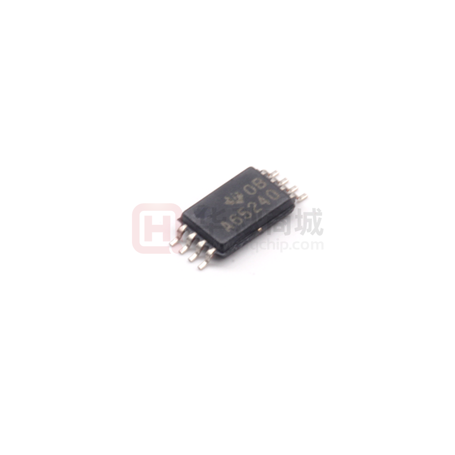
SN65220, SN65240, SN75240
SLLS266J – FEBRUARY 1997 – REVISED AUGUST 2022
SNx52x0 USB Port Transient Suppressors
1 Features
3 Description
•
The SN65220 device is a dual, and the SN65240
and SN75240 devices are quadruple, unidirectional
transient voltage suppressors (TVS). These devices
provide electrical noise transient protection to
Universal Serial Bus (USB) low and full-speed ports.
The input capacitance of 35 pF makes it unsuitable for
high-speed USB 2.0 applications.
•
•
•
•
Any cabled I/O can be subjected to electrical
noise transients from various sources. These noise
transients can cause damage to the USB transceiver
or the USB ASIC if they are of sufficient magnitude
and duration.
2 Applications
•
•
USB full-speed host, HUB, or peripheral
Ports
The SN65220, SN65240, and SN75240 devices
ESD performance is measured at the system level,
according to IEC61000-4-2; system design, however,
impacts the results of these tests. To accomplish
a high compliance level, careful board design and
layout techniques are required.
Device Information(1)
PART NUMBER
SN65220
SN65240
SN75240
(1)
PACKAGE
BODY SIZE (NOM)
SOT-23 (6)
2.90 mm × 1.60 mm
DSBGA (4)
0.925 mm × 0.925 mm
PDIP (8)
9.09 mm × 6.35 mm
TSSOP (8)
3.00 mm × 4.40 mm
See the orderable addendum at the end of the data sheet for
all available packages.
7.5
USB
Transceiver
5
27
D+
A
15 k
GND
SN65220 or ½
SNx5240
Current – A
•
Design to protect submicron 3-V or 5-V
circuits from noise transients
Port ESD protection capability exceeds:
– 15-kV human body model
– 2-kV machine model
Available in a WCSP chip-scale package
Stand-off voltage: 6 V (minimum)
Low current leakage: 1-µA maximum at 6 V
Low capacitance: 35-pF (typical)
2.5
0
-2.5
-5
15 k
-7.5
B
27
Simplified Schematic
D-
-10
-10
-5
0
5
10
Voltage – V
15
TVS Current vs Voltage
An IMPORTANT NOTICE at the end of this data sheet addresses availability, warranty, changes, use in safety-critical applications,
intellectual property matters and other important disclaimers. PRODUCTION DATA.
�SN65220, SN65240, SN75240
www.ti.com
SLLS266J – FEBRUARY 1997 – REVISED AUGUST 2022
Table of Contents
1 Features............................................................................1
2 Applications..................................................................... 1
3 Description.......................................................................1
4 Revision History.............................................................. 2
5 Device Comparison Table...............................................3
6 Pin Configuration and Functions...................................3
7 Specifications.................................................................. 4
7.1 Absolute Maximum Ratings........................................ 4
7.2 ESD Ratings............................................................... 4
7.3 Recommended Operating Conditions.........................4
7.4 Thermal Information....................................................4
7.5 Electrical Characteristics.............................................4
7.6 Typical Characteristics................................................ 5
8 Parameter Measurement Information............................ 5
9 Detailed Description........................................................6
9.1 Overview..................................................................... 6
9.2 Functional Block Diagram........................................... 6
9.3 Feature Description.....................................................7
9.4 Device Functional Modes............................................7
10 Application and Implementation.................................. 8
10.1 Application Information............................................. 8
10.2 Typical Application.................................................... 8
11 Power Supply Recommendations..............................10
12 Layout...........................................................................10
12.1 Layout Guidelines................................................... 10
12.2 Layout Example...................................................... 10
13 Device and Documentation Support..........................11
13.1 Receiving Notification of Documentation Updates.. 11
13.2 Support Resources................................................. 11
13.3 Trademarks............................................................. 11
13.4 Electrostatic Discharge Caution.............................. 11
13.5 Glossary.................................................................. 11
14 Mechanical, Packaging, and Orderable
Information.................................................................... 11
4 Revision History
NOTE: Page numbers for previous revisions may differ from page numbers in the current version.
Changes from Revision I (April 2021) to Revision J (August 2022)
Page
• Updated the SN65220, SN65240, and SN75240 suppressors in the Device Comparison table........................3
Changes from Revision H (May 2015) to Revision I (April 2021)
Page
• Updated the numbering format for tables, figures and cross-references throughout the document ..................1
• Updated the units for resistance from O to Ω in the Simplified Schematic figure............................................... 1
• Updated the units from O to Ω in the Typical Application Schematic for ESD Protection of USB Transceivers
figure ..................................................................................................................................................................8
• Updated the units from O to Ω in the Layout Example of a 4-Layer Board With SN65220 figure.................... 10
Changes from Revision G (August 2008) to Revision H (May 2015)
Page
• Added Pin Configuration and Functions section, ESD table, Thermal Information table, Feature Description
section, Device Functional Modes, Application and Implementation section, Power Supply Recommendations
section, Layout section, Device and Documentation Support section, and Mechanical, Packaging, and
Orderable Information section ........................................................................................................................... 1
2
Submit Document Feedback
Copyright © 2022 Texas Instruments Incorporated
Product Folder Links: SN65220 SN65240 SN75240
�SN65220, SN65240, SN75240
www.ti.com
SLLS266J – FEBRUARY 1997 – REVISED AUGUST 2022
5 Device Comparison Table
PRODUCT
SUPPRESSORS
TA - RANGE
PACKAGE
SN65220
2
–40°C to 85°C
SN65240
4
–40°C to 85°C
SN75240
4
0°C to 70°C
WCSP-4
SOT23-6
DIP-8
TSSOP-8
DIP-8
TSSOP-8
6 Pin Configuration and Functions
1
GND
2
NC
3
SADI
NC
6
A
5
GND
4
B
GND
C
GND
D
8
7
6
5
1
2
3
4
A
GND
B
GND
Figure 6-2. P, PW Package,s 8-Pin PDIP, TSSOP
(Top View)
Figure 6-1. DBV Package, 6-Pin SOT-23 (Top View)
Table 6-1. Pin Functions
PIN
TYPE
DESCRIPTION
NAME
DBV
P, PW
A
6
8
Analog input
Transient suppressor input – Line 1
B
4
6
Analog input
Transient suppressor input – Line 2
C
—
2
Analog input
Transient suppressor input – Line 3
D
—
4
Analog input
Transient suppressor input – Line 4
GND
2, 5
1, 3, 5, 7
Power
NC
1, 3
—
—
Local device ground
Internally not connected
A
A1
A2
GND
B
B1
B2
GND
Figure 6-3. YZB Package, 4-Pin DSBGA (Top View)
Table 6-2. Pin Functions
PIN
TYPE
DESCRIPTION
NO.
NAME
A1
A
Analog input
Transient suppressor input – Line 1
B1
B
Analog input
Transient suppressor input – Line 2
A2, B2
GND
Power
Local device ground
Submit Document Feedback
Copyright © 2022 Texas Instruments Incorporated
Product Folder Links: SN65220 SN65240 SN75240
3
�SN65220, SN65240, SN75240
www.ti.com
SLLS266J – FEBRUARY 1997 – REVISED AUGUST 2022
7 Specifications
7.1 Absolute Maximum Ratings
over operating free-air temperature range (unless otherwise noted)(1)
MIN
MAX
UNIT
60
W
Peak forward surge current
3
A
Peak reverse surge current
–9
A
150
°C
PD(peak)
Peak power dissipation
IFSM
IRSM
Tstg
Storage temperature
(1)
–65
Stresses beyond those listed under Absolute Maximum Ratings may cause permanent damage to the device. These are stress ratings
only, and functional operation of the device at these or any other conditions beyond those indicated under Section 7.3 is not implied.
Exposure to absolute-maximum-rated conditions for extended periods may affect device reliability.
7.2 ESD Ratings
VALUE
V(ESD)
(1)
(2)
Electrostatic discharge
Human body model (HBM), per ANSI/ESDA/JEDEC JS-001, all pins(1)
±15000
Charged device model (CDM), per JEDEC specification JESD22-C101, all
pins(2)
±2000
UNIT
V
JEDEC document JEP155 states that 500-V HBM allows safe manufacturing with a standard ESD control process.
JEDEC document JEP157 states that 250-V CDM allows safe manufacturing with a standard ESD control process.
7.3 Recommended Operating Conditions
MIN
TA
Ambient temperature
SN75240
SN65220, SN65240
MAX UNIT
0
70
–40
85
°C
7.4 Thermal Information
SN65220
THERMAL METRIC(1)
SN65240, SN75240
DBV
(SOT-23)
YZB
(DSBGA)
P
(PDIP)
6 PINS
4 BALLS
RθJA
Junction-to-ambient thermal resistance
199.5
170
67.5
RθJC(top)
Junction-to-case (top) thermal resistance
159.7
1.8
RθJB
Junction-to-board thermal resistance
51.1
43.5
ψJT
Junction-to-top characterization parameter
41
9.2
ψJB
Junction-to-board characterization parameter
50.5
43.5
(1)
PW
(TSSOP)
UNIT
8 PINS
185.3
°C/W
57.9
68.8
°C/W
44.5
114.0
°C/W
36.2
9.9
°C/W
44.5
112.3
°C/W
For more information about traditional and new thermal metrics, see the Semiconductor and IC Package Thermal Metrics application
report, SPRA953.
7.5 Electrical Characteristics
over recommended operating conditions (unless otherwise noted)
PARAMETER
4
TEST CONDITIONS
Ilkg
Leakage current
VI = 6 V at A, B, C, or D terminals
V(BR)
Breakdown voltage
VI = 1 mA at A, B, C, or D terminals
CIN
Input capacitance to ground
VI = 0.4 sin (4E6πt) + 0.5 V
Submit Document Feedback
MIN
TYP
MAX
1
6.5
7
35
8
UNIT
µA
V
pF
Copyright © 2022 Texas Instruments Incorporated
Product Folder Links: SN65220 SN65240 SN75240
�SN65220, SN65240, SN75240
www.ti.com
SLLS266J – FEBRUARY 1997 – REVISED AUGUST 2022
7.6 Typical Characteristics
TA = 25°C unless otherwise noted.
7.5
5
TVS Current – A
2.5
0
-2.5
-5
-7.5
-10
-10
-5
0
5
TVS Voltage – V
10
15
Figure 7-1. Transient-Voltage-Suppressor Current vs Voltage
8 Parameter Measurement Information
ILK
VI
DUT
Figure 8-1. Measurement of Leakage Current
II
VBR
DUT
Figure 8-2. Measurement of Breakdown Voltage
Submit Document Feedback
Copyright © 2022 Texas Instruments Incorporated
Product Folder Links: SN65220 SN65240 SN75240
5
�SN65220, SN65240, SN75240
www.ti.com
SLLS266J – FEBRUARY 1997 – REVISED AUGUST 2022
9 Detailed Description
9.1 Overview
The SN65220, SN65240, and SN75240 devices integrate multiple unidirectional transient voltage suppressors
(TVS). Figure 9-1 shows the equivalent circuit diagram of a single TVS diode.
For positive transient voltages, only the Q1 transistor determines the switching characteristic. When the input
voltage reaches the Zener voltage, VZ, Zener diode D1 conducts; therefore, allowing for the base-emitter
voltage, VBE, to increase. At VIN = VZ + VBE, the transistor starts conducting. From then on, its on-resistance
decreases linearly with increasing input voltage.
For negative transient voltages, only diode D2 determines the switching characteristic. Here, switching occurs
when the input voltage exceeds the diode forward voltage, VFW.
7.5
5
Current – A
A,B,C or D
D1
Q1
D2
R1
GND
2.5
VFW
VZ
VBE
0
-2.5
-5
Measured
from A,B,C
or D to GND
-7.5
-10
-10
-5
0
5
10
Voltage – V
15
Figure 9-1. TVS Structure and Current — Voltage Characteristic
9.2 Functional Block Diagram
SN65240
SN75240
A C
SN65220
A
GND
GND
GND
GND
GND
GND
B
6
B
D
Submit Document Feedback
Copyright © 2022 Texas Instruments Incorporated
Product Folder Links: SN65220 SN65240 SN75240
�www.ti.com
SN65220, SN65240, SN75240
SLLS266J – FEBRUARY 1997 – REVISED AUGUST 2022
9.3 Feature Description
The SN65220, SN65240, and SN75240 family of unidirectional transient voltage suppressors provide transient
protection to Universal Serial Bus low and full−speed ports. These TVS diodes provide a minimum breakdown
voltage of 6.5-V to protect USB transceivers and USB ASICs typically implemented in 3-V or 5-V digital CMOS
technology.
9.4 Device Functional Modes
TVS diodes possess two functional modes, a high-impedance and a conducting mode.
During normal operating conditions, that is in the absence of high voltage transients, the breakdown voltage of
TVS diodes is not exceeded and the devices remain high-impedance.
In the presence of high-voltage transients the breakdown voltage is exceeded. The TVS diodes then conduct
and become low-impedance. In this mode excessive transient energy is shunted directly to local circuit ground,
preventing USB transceivers from electrical damage.
Submit Document Feedback
Copyright © 2022 Texas Instruments Incorporated
Product Folder Links: SN65220 SN65240 SN75240
7
�SN65220, SN65240, SN75240
www.ti.com
SLLS266J – FEBRUARY 1997 – REVISED AUGUST 2022
10 Application and Implementation
Note
Information in the following applications sections is not part of the TI component specification,
and TI does not warrant its accuracy or completeness. TI’s customers are responsible for
determining suitability of components for their purposes, as well as validating and testing their design
implementation to confirm system functionality.
10.1 Application Information
The USB has become a popular solution to connect PC peripherals. The USB allows devices to be hot-plugged
in and out of the existing PC system without rebooting or turning off the PC. Because frequent human interaction
with the USB system occurs as a result of its attractive hot-plugging ability, there is the possibility for large
ESD strikes and damage to crucial system elements. The ESD protection included on the existing hardware
is typically in the 2-kV to 4-kV range for the human body model (HBD) and 200-V to 300-V for the machine
model (MM). The ESD voltage levels found in a normal USB operating environment can exceed these levels.
The SN75240, SN65240, and SN65220 devices will increase the robustness of the existing USB hardware to
ESD strikes common to the environment in which USB is likely to be used.
10.2 Typical Application
Figure 10-1 shows a typical USB system and application of the SN75240, SN65240, and SN65220 devices.
Connections to pin A from the D+ data line, pin B from the D– data line, and the device grounds from the GND
line that already exists are necessary to increase the amount of ESD protection provided to the USB port.
The design of the suppressor gives it very low maximum current leakage of 1 μA, a very low typical capacitance
of 35 pF, and a standoff voltage minimum of 6 V. Because of these levels, the SN75240, SN65240, and
SN65220 devices will provide added protection to the USB system hardware during ESD events without
introducing the high capacitance and current leakage levels typical of external transient voltage suppressors.
The addition of an SN75240, SN65240, or SN65220 device is beneficial to both full-speed and low-speed USB
1.1 bandwidth standards.
USB down stream
transceiver
USB hub port
transceiver
1.5 k�(1)
27 �
D+
D+
A
27 �
A
15 k�
GND
SN65220 or ½
SNx5240
GND
SN65220 or ½
SNx5240
15 k�
1.5 k�(2)
B
D-
D-
B
1) Full-speed only 27 �
2) Low-speed only
27
Figure 10-1. Typical Application Schematic for ESD Protection of USB Transceivers
8
Submit Document Feedback
Copyright © 2022 Texas Instruments Incorporated
Product Folder Links: SN65220 SN65240 SN75240
�SN65220, SN65240, SN75240
www.ti.com
SLLS266J – FEBRUARY 1997 – REVISED AUGUST 2022
10.2.1 Design Requirements
For this design example, use the parameters listed in Table 10-1 as design parameters.
Table 10-1. Design Parameters
DESIGN PARAMETER
EXAMPLE VALUE
Minimum breakdown voltage (TVS)
6.5 V
Maximum supply voltage (USB transceiver)
5.5 V
Typical junction capacitance (TVS)
35 pF
Maximum data rate (USB transceiver)
12 Mbps
10.2.2 Detailed Design Procedure
To effectively protect USB transceivers, use TVS diodes with breakdown voltages close to 6 V, such as the
SN65220, SN65240, or SN75220 devices.
Because of the TVS junction capacitance of 35 pF, apply these TVS diodes only to USB transceivers with
full-speed capability that is 12 Mbps maximum.
Place the TVS diodes as close to the board connector as possible to prevent transient energies from entering
further board space.
Connect the TVS diode between the data lines (D+, D–) and local circuit ground (GND).
Because noise transient represents high-speed frequencies, ensure low-inductance return paths for the transient
currents by providing a solid ground plane and using two VIAs connecting the TVS terminals to ground.
10.2.3 Application Curve
Ipk
I(A)
90%
Ipk
10%
Ipk
tr
Time
Figure 10-2. HBM Curve
Submit Document Feedback
Copyright © 2022 Texas Instruments Incorporated
Product Folder Links: SN65220 SN65240 SN75240
9
�SN65220, SN65240, SN75240
www.ti.com
SLLS266J – FEBRUARY 1997 – REVISED AUGUST 2022
11 Power Supply Recommendations
Unlike other semiconductor components that require a supply voltage to operate, the SN65220, SN65240,
and SN75240 transient suppressors are combinations of multiple p-n diodes, activated by transient voltages.
Therefore, these transient suppressors do not require external voltage supplies.
12 Layout
12.1 Layout Guidelines
The multiple ground pins provided lower the connection resistance to ground. In order to improve circuit
operation, a connection to all ground pins must be provided on the system printed circuit board. Without proper
device connection to ground, the speed and protection capability of the device will be degraded.
•
•
•
The ground termination pads should be connected directly to a ground plane on the board for optimum
performance. A single trace ground conductor will not provide an effective path for fast rise-time transient
events including ESD due to parasitic inductance.
Nominal inductive values of a PCB trace are approximately 20 nH/cm. This value may seem small, but an
apparent short length of trace may be sufficient to produce significant L(di/dt) effects with fast rise-time ESD
spikes.
Mount the TVS as close as possible to the I/O socket to reduce radiation originating from the transient as it is
routed to ground.
Note
Direct connective paths of the traces are taken to the suppressor mounting pads to minimize parasitic
inductance in the surge-current conductive path, thus minimizing L(di/dt) effects.
12.2 Layout Example
VIA to Power Ground Plane
USB
Connector
VIA to Power Supply Plane
GND
USB
Transceiver
15 k
27
NC
27
SN65220
A
GND
GND
NC
B
D+
D-
15 k
VBUS
Figure 12-1. Layout Example of a 4-Layer Board With SN65220
10
Submit Document Feedback
Copyright © 2022 Texas Instruments Incorporated
Product Folder Links: SN65220 SN65240 SN75240
�SN65220, SN65240, SN75240
www.ti.com
SLLS266J – FEBRUARY 1997 – REVISED AUGUST 2022
13 Device and Documentation Support
13.1 Receiving Notification of Documentation Updates
To receive notification of documentation updates, navigate to the device product folder on ti.com. Click on
Subscribe to updates to register and receive a weekly digest of any product information that has changed. For
change details, review the revision history included in any revised document.
13.2 Support Resources
TI E2E™ support forums are an engineer's go-to source for fast, verified answers and design help — straight
from the experts. Search existing answers or ask your own question to get the quick design help you need.
Linked content is provided "AS IS" by the respective contributors. They do not constitute TI specifications and do
not necessarily reflect TI's views; see TI's Terms of Use.
13.3 Trademarks
TI E2E™ is a trademark of Texas Instruments.
All trademarks are the property of their respective owners.
13.4 Electrostatic Discharge Caution
This integrated circuit can be damaged by ESD. Texas Instruments recommends that all integrated circuits be handled
with appropriate precautions. Failure to observe proper handling and installation procedures can cause damage.
ESD damage can range from subtle performance degradation to complete device failure. Precision integrated circuits may
be more susceptible to damage because very small parametric changes could cause the device not to meet its published
specifications.
13.5 Glossary
TI Glossary
This glossary lists and explains terms, acronyms, and definitions.
14 Mechanical, Packaging, and Orderable Information
The following pages include mechanical, packaging, and orderable information. This information is the most
current data available for the designated devices. This data is subject to change without notice and revision of
this document. For browser-based versions of this data sheet, refer to the left-hand navigation.
Submit Document Feedback
Copyright © 2022 Texas Instruments Incorporated
Product Folder Links: SN65220 SN65240 SN75240
11
�PACKAGE OPTION ADDENDUM
www.ti.com
14-Oct-2022
PACKAGING INFORMATION
Orderable Device
Status
(1)
Package Type Package Pins Package
Drawing
Qty
Eco Plan
(2)
Lead finish/
Ball material
MSL Peak Temp
Op Temp (°C)
Device Marking
(3)
Samples
(4/5)
(6)
SN65220DBVR
ACTIVE
SOT-23
DBV
6
3000
RoHS & Green
NIPDAU
Level-1-260C-UNLIM
-40 to 85
SADI
Samples
SN65220DBVRG4
ACTIVE
SOT-23
DBV
6
3000
RoHS & Green
NIPDAU
Level-1-260C-UNLIM
-40 to 85
SADI
Samples
SN65220DBVT
ACTIVE
SOT-23
DBV
6
250
RoHS & Green
NIPDAU
Level-1-260C-UNLIM
-40 to 85
SADI
Samples
SN65220DBVTG4
ACTIVE
SOT-23
DBV
6
250
RoHS & Green
NIPDAU
Level-1-260C-UNLIM
-40 to 85
SADI
Samples
SN65240P
ACTIVE
PDIP
P
8
50
RoHS & Green
NIPDAU
N / A for Pkg Type
-40 to 85
SN65240P
Samples
SN65240PW
ACTIVE
TSSOP
PW
8
150
RoHS & Green
NIPDAU
Level-1-260C-UNLIM
-40 to 85
A65240
Samples
SN65240PWG4
ACTIVE
TSSOP
PW
8
150
RoHS & Green
NIPDAU
Level-1-260C-UNLIM
-40 to 85
A65240
Samples
SN65240PWR
ACTIVE
TSSOP
PW
8
2000
RoHS & Green
NIPDAU
Level-1-260C-UNLIM
-40 to 85
A65240
Samples
SN75240P
ACTIVE
PDIP
P
8
50
RoHS & Green
NIPDAU
N / A for Pkg Type
0 to 70
SN75240P
Samples
SN75240PW
ACTIVE
TSSOP
PW
8
150
RoHS & Green
NIPDAU
Level-1-260C-UNLIM
0 to 70
A75240
Samples
SN75240PWG4
ACTIVE
TSSOP
PW
8
150
RoHS & Green
NIPDAU
Level-1-260C-UNLIM
0 to 70
A75240
Samples
SN75240PWR
ACTIVE
TSSOP
PW
8
2000
RoHS & Green
NIPDAU
Level-1-260C-UNLIM
0 to 70
A75240
Samples
SN75240PWRG4
ACTIVE
TSSOP
PW
8
2000
RoHS & Green
NIPDAU
Level-1-260C-UNLIM
0 to 70
A75240
Samples
(1)
The marketing status values are defined as follows:
ACTIVE: Product device recommended for new designs.
LIFEBUY: TI has announced that the device will be discontinued, and a lifetime-buy period is in effect.
NRND: Not recommended for new designs. Device is in production to support existing customers, but TI does not recommend using this part in a new design.
PREVIEW: Device has been announced but is not in production. Samples may or may not be available.
OBSOLETE: TI has discontinued the production of the device.
(2)
RoHS: TI defines "RoHS" to mean semiconductor products that are compliant with the current EU RoHS requirements for all 10 RoHS substances, including the requirement that RoHS substance
do not exceed 0.1% by weight in homogeneous materials. Where designed to be soldered at high temperatures, "RoHS" products are suitable for use in specified lead-free processes. TI may
reference these types of products as "Pb-Free".
RoHS Exempt: TI defines "RoHS Exempt" to mean products that contain lead but are compliant with EU RoHS pursuant to a specific EU RoHS exemption.
Green: TI defines "Green" to mean the content of Chlorine (Cl) and Bromine (Br) based flame retardants meet JS709B low halogen requirements of


 工商网监
湘ICP备2023018690号
工商网监
湘ICP备2023018690号


