SN65LVCP204
www.ti.com ................................................................................................................................................................................................... SLLS913 – MARCH 2009
Gigabit 4 × 4 CROSSPOINT SWITCH
•
•
•
•
•
•
•
•
•
•
The SN65LVCP204 is characterized for operation
from –40°C to 85°C.
3DE
Up to 2.5-Gbps Operation
Non-Blocking Architecture Allows Each
Output to Be Connected to Any Input
30 ps of Deterministic Jitter
Selectable Transmit Preemphasis Per Lane
Selectable Receive Equalization
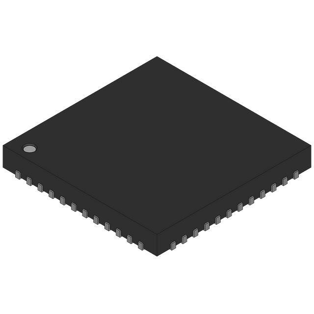
Available Packaging: 48-Pin QFN
Propagation Delay Times: 500 ps Typical
Inputs Electrically Compatible With
CML Signal Levels
Operates From a Single 3.3-V Supply
Ability to Place Ouputs in High-Impedance
State
Low Power: 560 mW
Integrated Termination Resistors
2DE
•
•
1DE
FEATURES
1
4DE
APPLICATIONS
•
•
•
•
Clock Buffering/Clock MUXing
Wireless Base Stations
High-Speed Network Routing
Telecom/Datacom
DESCRIPTION
The SN65LVCP204 is a 4×4 non-blocking crosspoint
switch in a flow-through pinout that allows for ease in
PCB layout. VML signaling is used to achieve a
high-speed data throughput while using low power.
Each of the output drivers includes a 4:1 multiplexer
to allow any input to be routed to any output. Internal
signal paths are fully differential to achieve high
signaling speeds while maintaining low signal skews.
The SN65LVCP204 incorporates 100-Ω termination
resistors for those applications where board space is
at a premium. Transmit preemphasis and receive
equalization are built in for superior signal integrity
performance.
1
Please be aware that an important notice concerning availability, standard warranty, and use in critical applications of Texas
Instruments semiconductor products and disclaimers thereto appears at the end of this data sheet.
PRODUCTION DATA information is current as of publication date.
Products conform to specifications per the terms of the Texas
Instruments standard warranty. Production processing does not
necessarily include testing of all parameters.
Copyright © 2009, Texas Instruments Incorporated
�SN65LVCP204
SLLS913 – MARCH 2009 ................................................................................................................................................................................................... www.ti.com
These devices have limited built-in ESD protection. The leads should be shorted together or the device placed in conductive foam
during storage or handling to prevent electrostatic damage to the MOS gates.
LOGIC DIAGRAM
VBB
1A
EQ
RT
RT
2
EQ
S10
S11
P11
P12
00
1B
2
01
10
11
VBB
2A
1Y
1Z
4x1
MUX
1DE
EQ
RT
RT
2
00
EQ
P21
P22
S20
S21
2
2Y
2Z
01
2B
10
11
VBB
3A
2
EQ
RT
RT
00
EQ
10
11
2
4A
EQ
00
RT
RT
2DE
S30
S31
P31
P32
2
01
3B
VBB
4x1
MUX
3Y
3Z
4x1
MUX
3DE
P41
P42
S40
S41
2
4Y
4Z
01
10
EQ
11
4x1
MUX
4DE
4B
e
-W
-W
TERMINAL FUNCTIONS
TERMINAL
NAME
TYPE
NO.
DESCRIPTION
High Speed I/O
Differential inputs (with 50-Ω
termination to VBB)
xA = P; xB = N
Line-side differential inputs, CML compatible
41, 34, 31, 28
40, 33, 30, 27
Differential output xY = P; xZ = N
Switch-side differential outputs, VML
45, 38, 37, 25
Input
Data enable; active low; LVTTL; when not enabled, the ouput
is in the high-impedance state for power savings.
Input; S1x = channel 1, bit x
Switching selection; LVTTL
xA
xB
3, 6, 9, 16
4, 7, 10, 17
xY
xZ
Control Signals
xDE
S10–S41
2
47, 48, 1, 2, 13,
14, 19, 20
Submit Documentation Feedback
Copyright © 2009, Texas Instruments Incorporated
Product Folder Link(s): SN65LVCP204
�SN65LVCP204
www.ti.com ................................................................................................................................................................................................... SLLS913 – MARCH 2009
TERMINAL FUNCTIONS (continued)
TERMINAL
NAME
P11–P42
EQ
TYPE
NO.
43, 44, 35, 36, 23,
24, 21, 22
11
DESCRIPTION
Input; P1x = channel 1, bit x
Output preemphasis control; LVTTL
Input; selection for receive
equalization setting
EQ = 1 (default) is for the 5-dB setting, EQ = 0 is for the 12-dB
setting
Power
Power supply 3.3 V ±5%
Power Supply
VCC
8, 18, 29, 39, 46
GND
5, 15, 26, 32, 42
Ground
The ground center pad of the package must be connected to
GND plane.
Thermal pad
VBB
12
Input
Receiver input biasing voltage
EQUIVALENT INPUT AND OUTPUT SCHEMATIC DIAGRAMS
VCC
IN+
RT(SE)
= 50 W
Gain
Stage
+ EQ
VCC
RBBDC
RT(SE)
= 50 W
IN−
VBB
ESD
LineEndTermination
Self−Biasing Network
Figure 1. Equivalent Input Circuit Design
OUT+
49.9 W
OUT−
49.9 W
VOCM
1 pF
Figure 2. Common-Mode Output Voltage Test Circuit
Submit Documentation Feedback
Copyright © 2009, Texas Instruments Incorporated
Product Folder Link(s): SN65LVCP204
3
�SN65LVCP204
SLLS913 – MARCH 2009 ................................................................................................................................................................................................... www.ti.com
Table 1. CROSSPOINT LOGIC TABLES
OUTPUT CHANNEL 1
CONTROL
PINS
INPUT
SELECTED
OUTPUT CHANNEL 2
CONTROL
PINS
INPUT
SELECTED
OUTPUT CHANNEL 3
CONTROL
PINS
OUTPUT CHANNEL 4
INPUT
SELECTED
CONTROL
PINS
INPUT
SELECTED
S10
S11
1Y/1Z
S20
S21
2Y/2Z
S30
S31
3Y/3Z
S40
S41
4Y/4Z
0
0
1A/1B
0
0
1A/1B
0
0
1A/1B
0
0
1A/1B
0
1
2A/2B
0
1
2A/2B
0
1
2A/2B
0
1
2A/2B
1
0
3A/3B
1
0
3A/3B
1
0
3A/3B
1
0
3A/3B
1
1
4A/4B
1
1
4A/4B
1
1
4A/4B
1
1
4A/4B
AVAILABLE OPTIONS
(1)
TA
DESCRIPTION
–40°C to 85°C
Serial multiplexer
PACKAGED DEVICE (1)
RGZ (48-Pin) (Orderable)
SN65LVCP204RGZ
The package is available taped and reeled. Add an R suffix to device types (e.g., SN65LVCP204RGZR).
PACKAGE THERMAL CHARACTERISTICS
PACKAGE THERMAL CHARACTERISTICS (1)
NOM
UNIT
33
°C/W
θJA (junction-to-ambient)
θJB (junction-to-board)
θJC (junction-to-case)
Ψ-jt (junction-to-top pseudo)
Ψ-jb (junction-to-board pseudo)
Four-layer JEDEC board (JESD51-7) using eight GND-vias of 0.3-mm
diameter on the center pad as shown in the section: Recommended
PCB footprint with boundary and environment conditions of JEDEC
board (JESD51-2)
20
°C/W
23.6
°C/W
0.6
°C/W
19.4
°C/W
5.4
°C/W
θJP (junction-to-pad)
(1)
See the IC Package Thermal Metrics application report SPRA953 for a detailed explanation of thermal parameters.
ABSOLUTE MAXIMUM RATINGS
over operating free-air temperature range (unless otherwise noted) (1)
UNIT
VCC
Supply-voltage range (2)
–0.5 V to 6 V
Control inputs, all outputs
Voltage range
ESD
TJ
Receiver inputs
All pins
3 kV
Charged-device model (4)
All pins
500 V
See Package Thermal Characteristics
table
Maximum junction temperature
2
Reflow temperature package soldering, 4 seconds
(2)
(3)
(4)
4
–0.5 V to 4 V
Human-body model (3)
Moisture sensitivity level
(1)
–0.5 V to (VCC + 0.5 V)
260°C
Stresses beyond those listed under absolute maximum ratings may cause permanent damage to the device. These are stress ratings
only and functional operation of the device at these or any other conditions beyond those indicated under recommended operating
conditions is not implied. Exposure to absolute-maximum-rated conditions for extended periods may affect device reliability.
All voltage values, except differential I/O bus voltages, are with respect to the ground terminals.
Tested in accordance with JEDEC Standard 22, Test Method A114-A.
Tested in accordance with JEDEC Standard 22, Test Method C101.
Submit Documentation Feedback
Copyright © 2009, Texas Instruments Incorporated
Product Folder Link(s): SN65LVCP204
�SN65LVCP204
www.ti.com ................................................................................................................................................................................................... SLLS913 – MARCH 2009
RECOMMENDED OPERATING CONDITIONS
dR
Operating data rate
VCC
Supply voltage
VCC(N)
Supply-voltage noise amplitude
TJ
Junction temperature
TA
Operating free-air temperature (1)
MIN
NOM
MAX
UNIT
2.5
Gbps
3.135
3.3
3.465
10 Hz to 1.25 GHz
V
20
mV
125
°C
–40
85
°C
dR(in) ≤ 1.25 Gbps
100
1750
mVPP
1.25 Gbps < dR(in) ≤ 2.5 Gbps
100
1560
mVPP
dR(in) > 2.5 Gbps
100
1000
mVPP
Note: for best jitter performance, ac
coupling is recommended.
1.5
DIFFERENTIAL INPUTS
Receiver peak-to-peak differential input
voltage (2)
VID
VICM
Receiver common-mode
input voltage
|V
VCC *
1.6
|
ID
2
V
CONTROL INPUTS
VIH
High-level input voltage
2
VCC + 0.3
V
VIL
Low-level input voltage
–0.3
0.8
V
120
Ω
DIFFERENTIAL OUTPUTS
RL
(1)
(2)
Differential load resistance
80
100
Maximum free-air temperature operation is allowed as long as the device maximum junction temperature is not exceeded.
Differential input voltage VID is defined as | IN+ – IN– |.
ELECTRICAL CHARACTERISTICS
over operating free-air temperature range (unless otherwise noted)
PARAMETER
TEST CONDITIONS
MIN
TYP (1)
MAX
UNIT
DIFFERENTIAL INPUTS
VIT+
Positive-going differential
input, high threshold
VIT–
Negative-going differential
input, low threshold
A(EQ)
Equalizer gain
RT(D)
Termination resistance,
differential
VBB
Open-circuit input voltage
(input self-bias voltage)
R(BBDC)
Biasing network dc
impedance
R(BBAC)
Biasing network ac
impedance
50
–50
at 1.25 GHz (EQ = 0)
mV
12
80
AC-coupled inputs
375 MHz
mV
100
dB
120
Ω
1.6
V
30
kΩ
42
Ω
650
mVPP
–650
mVPP
DIFFERENTIAL OUTPUTS
VODH
High-level output voltage
VODL
Low-level output voltage
VODB(PP)
Output differential voltage
without preemphasis (2)
VOCM
Output common-mode voltage
ΔVOC(SS)
Change in steady-state
common-mode output voltage
between logic states
(1)
(2)
RL = 100 Ω ±1%,
Px2 = Px1 = 0;
2.5 Gbps alternating 1010-pattern;
Figure 3
1000
1300
1500
1.65
See Figure 2
1
mVPP
V
mV
All typical values are at TA = 25°C and VCC = 3.3-V supply unless otherwise noted. They are for reference purposes and are not
production tested.
Differential output voltage V(ODB) is defined as | OUT+ – OUT– |.
Submit Documentation Feedback
Copyright © 2009, Texas Instruments Incorporated
Product Folder Link(s): SN65LVCP204
5
�SN65LVCP204
SLLS913 – MARCH 2009 ................................................................................................................................................................................................... www.ti.com
ELECTRICAL CHARACTERISTICS (continued)
over operating free-air temperature range (unless otherwise noted)
PARAMETER
TEST CONDITIONS
MIN
TYP (1)
Px2:Px1 = 00
0
Px2:Px1 = 01
3
Px2:Px1 = 10
6
Px2:Px1 = 11
9
MAX
UNIT
Output preemphasis voltage
V
ODB(PP)
VODPE(PP)
ratio,
RL = 100 Ω±1%;
x = L or S;
See Figure 3
t(PRE)
Preemphasis duration
measurement
Output preemphasis is set to 9 dB during test;
Pxx = 1;
Measured with a 100-MHz clock signal;
RL = 100 Ω ±1%, See Figure 4
175
ps
RO
Output resistance
Differential on-chip termination between OUT+ and
OUT–
100
Ω
V(PE)
dB
CONTROL INPUTS
IIH
High-level input current
VIN = VCC
IIL
Low-level input current
VIN = GND
R(PU)
Pullup resistance
5
–125
µA
–90
µA
35
kΩ
POWER CONSUMPTION
PD
Device power dissipation
All outputs terminated 100 Ω
PZ
Device power dissipation in
high-impedance state
ICC
Device current consumption
560
750
mW
All outputs in high-impedance state
600
mW
All outputs terminated 100 Ω
PRBS 27 – 1 pattern at 2.5 Gbps
220
mA
TYP (1)
MAX
UNIT
3
6
ns
0.5
0.7
ns
0.5
0.7
ns
SWITCHING CHARACTERISTICS
over operating free-air temperature range (unless otherwise noted)
PARAMETER
TEST CONDITIONS
MIN
MULTIPLEXER
t(SM)
Multiplexer switch time
Multiplexer to valid output
DIFFERENTIAL OUTPUTS
tPLH
Low-to-high propagation
delay
tPHL
High-to-low propagation
delay
tr
Rise time
tf
Fall time
tsk(p)
Pulse skew, | tPHL – tPLH | (2)
tsk(o)
Output skew
(3)
tsk(pp)
Part-to-part skew (4)
tzd
Switch time, hi-Z state to
disable
tze
RJ
(1)
(2)
(3)
(4)
6
Propagation delay, input to output
See Figure 6
20% to 80% of VO(DB); test pattern: 100-MHz clock signal;
see Figure 5 and Figure 8
110
ps
110
ps
20
ps
100
ps
300
ps
50 Ω to Vcm and 150-pF load on each output
20
ns
Switch time, hi-Z state to
enable
50 Ω to Vcm and 150-pF load on each output
10
ns
Device random jitter, rms
See Figure 8 for test circuit.
BERT setting 10–15
Alternating 10-pattern.
2
ps-rms
All outputs terminated with 100 Ω
25
0.8
All typical values are at 25°C and with 3.3-V supply, unless otherwise noted.
tsk(p) is the magnitude of the time difference between the tPLH and tPHL of any output of a single device.
tsk(o) is the magnitude of the time difference between the tPLH and tPHL of any two outputs of a single device.
tsk(pp) is the magnitude of the difference in propagation delay times between any specified terminals of two devices when both devices
operate with the same supply voltages, at the same temperature, and have identical packages and test circuits.
Submit Documentation Feedback
Copyright © 2009, Texas Instruments Incorporated
Product Folder Link(s): SN65LVCP204
�SN65LVCP204
www.ti.com ................................................................................................................................................................................................... SLLS913 – MARCH 2009
SWITCHING CHARACTERISTICS (continued)
over operating free-air temperature range (unless otherwise noted)
PARAMETER
TEST CONDITIONS
0 dB preemphasis
Intrinsic deterministic device (PREx_x = 0);
jitter (5) (6), peak-to-peak
See Figure 8 for the test
circuit.
DJ
(5)
(6)
(7)
0 dB preemphasis
Absolute deterministic
(PREx_x = 0);
output jitter (7), peak-to-peak See Figure 8 for the test
circuit.
MIN
PRBS 27 – 1
pattern
7
PRBS 2 – 1
pattern
TYP (1)
2.5 Gbps
MAX
30
1.25 Gbps;
EQ = 1
Over 25-inch
(63,5-cm)
FR4 trace
7
UNIT
ps
ps
Intrinsic deterministic device jitter is a measurement of the deterministic jitter contribution from the device. It is derived by the equation
(DJ(OUT) – DJ(IN)), where DJ(OUT) is the total peak-to-peak deterministic jitter measured at the output of the device in PSPP. DJ(IN) is the
peak-to-peak deterministic jitter of the pattern generator driving the device.
The SN65LVCP204 built-in passive input equalizer compensates for ISI. For a 25-inch (63,5-cm) FR4 transmission line with 8-mil
(0,2-mm) trace width, the SN65LVCP204 typically reduces jitter by 60 ps from the device input to the device output.
Absolute deterministic output jitter reflects the deterministic jitter measured at the SN65LVCP204 output. The value is a real value
measured with a bit-error tester as described in Figure 8. The absolute DJ reflects the sum of all deterministic jitter components
accumulated over the link: DJ(absolute) = DJ(Signal generator) + DJ(transmission line) + DJ(intrinsic(LVCP204)).
Table 2. Preemphasis Controls PL2, PL1, PS2, and PS1
(1)
Px2 (1)
Px1 (1)
OUTPUT
PREEMPHASIS
LEVEL IN dB
OUTPUT LEVEL IN mVpp
DE-EMPHASIZED
PREEMPHASIZED
TYPICAL FR4
TRACE LENGTH
0
0
0 dB
1200
1200
10 inches (25,4 cm) of FR4 trace
0
1
3 dB
850
1200
20 inches (50,8 cm) of FR4 trace
1
0
6 dB
600
1200
30 inches (76,2 cm) of FR4 trace
1
1
9 dB
425
1200
40 inches (101,6 cm) of FR4
trace
x = L or S
Table 3. Receive Equalization Settings
EQ
EQUALIZATION
1
5 dB
25 inches (63,5 cm) of FR4
TYPICAL TRACE
0
12 dB
43 inches (109,2 cm) of FR4
Submit Documentation Feedback
Copyright © 2009, Texas Instruments Incorporated
Product Folder Link(s): SN65LVCP204
7
�SN65LVCP204
SLLS913 – MARCH 2009 ................................................................................................................................................................................................... www.ti.com
PARAMETER MEASUREMENT INFORMATION
1−bit
1 to N bit
3−dB Preemphasis
VODPE3(pp)
9−dB Preemphasis
VOCM
VODB(PP)
VODPE2(pp)
6−dB Preemphasis
VODPE1(pp)
0−dB Preemphasis
VOH
VOL
Figure 3. Preemphasis and Output Voltage Waveforms and Definitions
1−bit
VODPE3(pp)
9−dB Preemphasis
1 to N bit
VODB(PP)
80%
20%
tPRE
Figure 4. t(PRE) Preemphasis Duration Measurement
80%
80%
VODB
20%
20%
tr
tf
Figure 5. Driver Output Transition Time
8
Submit Documentation Feedback
Copyright © 2009, Texas Instruments Incorporated
Product Folder Link(s): SN65LVCP204
�SN65LVCP204
www.ti.com ................................................................................................................................................................................................... SLLS913 – MARCH 2009
PARAMETER MEASUREMENT INFORMATION (continued)
VID = 0 V
IN
t PHLD
t PLHD
VOD = 0 V
OUT
Figure 6. Propagation Delay Input to Output
1/fO
1/fO
tjit(pp) = | tc(n) – 1/fO |
A.
All input pulses are supplied by an Agilent 81250 Stimulus System.
B.
The measurement is made with the AgilentParBert measurement software.
Figure 7. Driver Jitter Measurement Waveforms
DC
Block
DC
Block
Pattern
D+
Generator
Coax
SMA
DC
Block
D–
Coax
SMA
400-mVPP
Differential