SN65LVCP22
www.ti.com
SLLS553B – NOVEMBER 2002 – REVISED JUNE 2003
2x2 LVDS CROSSPOINT SWITCH
FEATURES
•
•
•
•
•
•
•
•
•
•
•
•
•
High Speed (>1000 Mbps) Upgrade for
DS90CP22 2x2 LVDS Crosspoint Switch
LVPECL Crosspoint Switch Available in
SN65LVCP23
Low-Jitter Fully Differential Data Path
50 ps (Typ), of Peak-to-Peak Jitter With PRBS
= 223–1 Pattern
Less Than 200 mW (Typ), 300 mW (Max) Total
Power Dissipation
Output (Channel-to-Channel) Skew Is 10 ps
(Typ), 50 ps (Max)
Configurable as 2:1 Mux, 1:2 Demux, Repeater
or 1:2 Signal Splitter
Inputs Accept LVDS, LVPECL, and CML
Signals
Fast Switch Time of 1.7 ns (Typ)
Fast Propagation Delay of 0.65 ns (Typ)
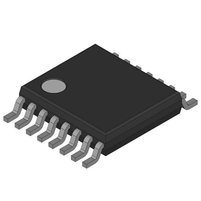
16 Lead SOIC and TSSOP Packages
Inter-Operates With TIA/EIA-644-A LVDS
Standard
Operating Temperature: –40°C to 85°C
APPLICATIONS
•
•
•
•
•
•
Base Stations
Add/Drop Muxes
Protection Switching for Serial Backplanes
Network Switches/Routers
Optical Networking Line Cards/Switches
Clock Distribution
DESCRIPTION
The SN65LVCP22 is a 2×2 crosspoint switch
providing greater than 1000 Mbps operation for each
path. The dual channels incorporate wide
common-mode (0 V to 4 V) receivers, allowing for the
receipt of LVDS, LVPECL, and CML signals. The
dual outputs are LVDS drivers to provide low-power,
low-EMI, high-speed operation. The SN65LVCP22
provides a single device supporting 2:2 buffering
(repeating), 1:2 splitting, 2:1 multiplexing, 2×2
switching, and LVPECL/CML to LVDS level
translation on each channel. The flexible operation of
the SN65LVCP22 provides a single device to support
the redundant serial bus transmission needs (working
and protection switching cards) of fault-tolerant switch
systems found in optical networking, wireless
infrastructure, and data commu- nications systems. TI
offers additional gigibit repeater/ translator and
crosspoint products in the SN65LVDS100 and
SN65LVDS122.
The SN65LVCP22 uses a fully differential data path
to ensure low-noise generation, fast switching times,
low pulse width distortion, and low jitter. Output
channel-to- channel skew is less than 10 ps (typ) and
50 ps (max) to ensure accurate alignment of outputs
in all applications. Both SOIC and TSSOP package
options are available to allow easy upgrade for
existing solutions, and board area savings where
space is critical.
OUTPUTS OPERATING SIMULTANEOUSLY
1 Gbps
223 -1 PRBS
OUTPUT 1
VCC = 3.3 V
|VID| = 200 mV, VIC = 1.2 V
Vertical Scale = 200 mV/div
OUTPUT 2
500 MHz
Horizontal Scale = 300 ps
Please be aware that an important notice concerning availability, standard warranty, and use in critical applications of Texas
Instruments semiconductor products and disclaimers thereto appears at the end of this data sheet.
PRODUCTION DATA information is current as of publication date.
Products conform to specifications per the terms of the Texas
Instruments standard warranty. Production processing does not
necessarily include testing of all parameters.
Copyright © 2002–2003, Texas Instruments Incorporated
�SN65LVCP22
www.ti.com
SLLS553B – NOVEMBER 2002 – REVISED JUNE 2003
These devices have limited built-in ESD protection. The leads should be shorted together or the device placed in conductive foam
during storage or handling to prevent electrostatic damage to the MOS gates.
ORDERING INFORMATION
(1)
PACKAGE DESIGNATOR
PART NUMBER (1)
SYMBOLIZATION
SOIC
SN65LVCP22D
LVCP22
TSSOP
SN65LVCP22PW
LVCP22
Add the suffix R for taped and reeled carrier
PACKAGE DISSIPATION RATINGS
(1)
(2)
PACKAGE
CIRCUIT BOARD
MODEL
TA ≤ 25°C
POWER RATING
DERATING FACTOR (1)
ABOVE TA = 25°C
TA = 85°C
POWER RATING
SOIC (D)
High-K (2)
1361 mW
13.9 mW/°C
544 mW
TSSOP (PW)
High-K (2)
1074 mW
10.7 mW/°C
430 mW
This is the inverse of the junction-to-ambient thermal resistance when board-mounted and with no air flow.
In accordance with the High-K thermal metric definitions of EIA/JESD51-7.
THERMAL CHARACTERISTICS
PARAMETER
TEST CONDITIONS
θJB
Junction-to-board thermal resistance
θJC
Junction-to-case thermal resistance
PD
Device power dissipation
VALUE
D
11.2
PW
18.4
D
23.7
PW
16.0
Typical
VCC = 3.3 V, TA = 25°C, 1 Gbps
198
Maximum
VCC = 3.6 V, TA = 85°C, 1 Gbps
313
FUNCTION TABLE
SEL0
SEL1
OUT0
OUT1
FUNCTION
0
0
IN0
IN0
1:2 Splitter
0
1
IN0
IN1
Repeater
1
0
IN1
IN0
Switch
1
1
IN1
IN1
1:2 Splitter
FUNCTIONAL BLOCK DIAGRAM
OUT 0
OUT 1
EN 0
EN 1
SEL 1
SEL 0
0
1
0
IN 0
IN 1
2
Submit Documentation Feedback
1
UNITS
°C/W
°C/W
mW
�SN65LVCP22
www.ti.com
SLLS553B – NOVEMBER 2002 – REVISED JUNE 2003
EQUIVALENT INPUT AND OUTPUT SCHEMATIC DIAGRAMS
INPUTS
VCC
IN +
IN -
400 Ω
SEL, EN
300 kΩ
7V
7V
7V
OUTPUTS
VCC
OUT +
OUT -
7V
7V
ABSOLUTE MAXIMUM RATINGS
over operating free-air temperature range unless otherwise noted (1)
UNITS
Supply voltage (2) range, VCC
–0.5 V to 4 V
CMOS/TTL input voltage (ENO, EN1, SEL0, SEL1)
–0.5 V to 4 V
LVDS receiver input voltage (IN+, IN–)
–0.7 V to 4.3 V
LVDS driver output voltage (OUT+, OUT–)
–0.5 V to 4 V
LVDS output short circuit current
Continuous
Storage temperature range
–65°C to 125°C
Lead temperature 1,6 mm (1/16 inch) from case for 10 seconds
Continuous power dissipation
Electrostatic discharge
(1)
(2)
(3)
(4)
235°C
See Dissipation Rating Table
Human body model (3)
All pins
±5 kV
Charged-device mode (4)
All pins
±500 V
Stresses beyond those listed under absolute maximum ratings may cause permanent damage to the device. These are stress ratings
only, and functional operation of the device at these or any other conditions beyond those indicated under recommended operating
conditions is not implied. Exposure to absolute-maximum-rated conditions for extended periods may affect device reliability.
All voltage values, except differential I/O bus voltages, are with respect to network ground terminals.
Tested in accordance with JEDEC Standard 22, Test Method A114-A.
Tested in accordance with JEDEC Standard 22, Test Method C101.
Submit Documentation Feedback
3
�SN65LVCP22
www.ti.com
SLLS553B – NOVEMBER 2002 – REVISED JUNE 2003
RECOMMENDED OPERATING CONDITIONS
MIN
Supply voltage, VCC
3
Receiver input voltage
0
NOM MAX
3.3
3.6
Junction temperature
UNIT
V
4
V
125
°C
Operating free-air temperature, TA (1)
–40
85
°C
Magnitude of differential input voltage |VID|
0.1
3
V
(1)
Maximum free-air temperature operation is allowed as long as the device maximum junction temperature is not exceeded.
INPUT ELECTRICAL CHARACTERISTICS
over recommended operatingconditions unless otherwise noted
PARAMETER
TEST CONDITIONS
TYP (1)
MIN
MAX
UNIT
CMOS/TTL DC SPECIFICATIONS (EN0, EN1, SEL0, SEL1)
VIH
High-level input voltage
2
VCC
VIL
Low-level input voltage
GND
0.8
V
IIH
High-level input current
VIN = 3.6 V or 2.0 V, VCC = 3.6 V
±20
µA
IIL
Low-level input current
VIN = 0.0 V or 0.8 V, VCC = 3.6 V
VCL
Input clamp voltage
ICL = –18 mA
±3
V
±1
±10
µA
-0.8
-1.5
V
LVDS OUTPUT SPECIFICATIONS (OUT0, OUT1)
RL = 75 Ω, See Figure 2
270
365
475
RL = 75 Ω, VCC = 3.3 V, TA = 25°C, See
Figure 2
285
365
440
Change in differential output voltage magnitude
between logic states
VID = ±100 mV, See Figure 2
–25
VOS
Steady-state offset voltage
See Figure 3
1
∆VOS
Change in steady-state offset voltage between
logic states
See Figure 3
–25
VOC(PP)
Peak-to-peak common-mode output voltage
See Figure 3
IOZ
High-impedance output current
VOUT = GND or VCC
IOFF
Power-off leakage current
VCC = 0 V, 1.5 V; VOUT = 3.6 V or GND
IOS
Output short-circuit current
VOUT+ or VOUT- = 0 V
IOSB
Both outputs short-circuit current
VOUT+ and VOUT- = 0 V
CO
Differential output capacitance
VI = 0.4 sin(4E6πt) + 0.5 V
|VOD|
Differential output voltage
∆|VOD|
25
1.2
50
–12
1.45
mV
mV
V
25
mV
150
mV
±10
µA
±10
µA
-24
mA
12
mA
3
pF
LVDS RECEIVER DC SPECIFICATIONS (IN0, IN1)
VTH
Positive-going differential input voltage threshold
See Figure 1 and Table 1
VTL
Negative-going differential input voltage threshold
See Figure 1 and Table 1
100
–100
VID(HYS) Differential input voltage hysteresis
VCMR
IIN
Input current
CIN
Differential input capacitance
mV
25
Common-mode voltage range
VID = 100 mV, VCC = 3.0 V to 3.6 V
mV
0.05
mV
3.95
VIN = 4 V, VCC = 3.6 V or 0.0
±1
±10
VIN = 0 V, VCC = 3.6V or 0.0
±1
±10
VI = 0.4 sin (4E6πt) + 0.5 V
3
V
µA
pF
SUPPLY CURRENT
ICCD
Total supply current
RL = 75 Ω, CL = 5 pF, 500 MHz (1000
Mbps), EN0=EN1=High
60
87
mA
ICCZ
3-state supply current
EN0 = EN1 = Low
25
35
mA
(1)
4
All typical values are at 25°C and with a 3.3-V supply.
Submit Documentation Feedback
�SN65LVCP22
www.ti.com
SLLS553B – NOVEMBER 2002 – REVISED JUNE 2003
SWITCHING CHARACTERISTICS
over recommended operating conditions unless otherwise noted
MIN
TYP
tSET
Input to SEL setup time
parameter
See Figure 6
1
0.5
ns
tHOLD
Input to SEL hold time
See Figure 6
1.1
0.5
ns
tSWITCH
SEL to switched output
See Figure 6
1.7
2.5
ns
tPHZ
Disable time, high-level-to-high-impedance
See Figure 5
2
4
ns
tPLZ
Disable time, low-level-to-high-impedance
See Figure 5
2
4
ns
tPZH
Enable time, high-impedance -to-high-level output
See Figure 5
2
4
ns
tPZL
Enable time, high-impedance-to-low-level output
See Figure 5
2
4
ns
tLHT
Differential output signal rise time (20%-80%) (1)
CL = 5 pF, See Figure 4
150
280
450
ps
CL = 5 pF, See Figure 4
150
tHLT
Differential output signal fall time
tJIT
TEST CONDITIONS
(20%-80%) (1)
Added peak-to-peak jitter
MAX
UNIT
280
450
ps
VID = 200 mV, 50% duty cycle,
VCM = 1.2 V, 500 MHz, CL = 5 pF
20
40
ps
VID = 200 mV, PRBS = 223-1 data pattern,
VCM = 1.2 V at 1000 Mbps, CL = 5 pF
50
105
ps
VID = 200 mV, 50% duty cycle,
VCM = 1.2 V at 500 MHz, CL = 5 pF
1.1
1.8
psRMS
400
650
1000
ps
400
tJrms
Added random jitter (rms)
tPLHD
Propagation delay time, low-to-high-level output (1)
tPHLD
Propagation delay time, high-to-low-level
output (1)
650
1000
ps
tskew
Pulse skew (|tPLHD– tPHLD|) (2)
CL = 5 pF, See Figure 4
20
100
ps
tCCS
Output channel-to-channel skew, splitter mode
CL = 5 pF, See Figure 4
10
50
ps
fMAX
(1)
(2)
(3)
Maximum operating
frequency (3)
1
GHz
Input: VIC = 1.2 V, VID = 200 mV, 50% duty cycle, 1 MHz, tr/tf = 500 ps
tskew is the magnitude of the time difference between the tPLHD and tPHLD of any output of a single device.
Signal generator conditions: 50% duty cycle, tr or tf ≤ 100 ps (10% to 90%), transmitter output criteria: duty cycle = 45% to 55% VOD ≥
300 mV.
PIN ASSIGNMENTS
D or PW PACKAGE
(TOP VIEW)
SEL1
SEL0
IN0+
IN0VCC
IN1+
IN1NC
1
2
3
4
5
6
7
8
16
15
14
13
12
11
10
9
EN0
EN1
OUT0+
OUT0GND
OUT1+
OUT1NC
NC - No internal connection
Submit Documentation Feedback
5
�SN65LVCP22
www.ti.com
SLLS553B – NOVEMBER 2002 – REVISED JUNE 2003
PARAMETER MEASUREMENT INFORMATION
IIN+
OUT +
IN+
VID
IN+ + IN-
VIC
VOD
VIN+
VIN-
2
VOY
IN-
OUT -
VOUT++ VOUT-
VOZ
IIN-
2
Figure 1. Voltage and Current Definitions
3.74 kΩ
Y
VOD
Z
+
_
75 Ω
0 V ≤ V(test) ≤ 2.4 V
3.74 kΩ
Figure 2. Differential Output Voltage (VOD) Test Circuit
IN+
OUT+
IN+
≈1.4 V
IN-
≈1 V
37.4 Ω ±1%
VID
VOC(PP)
IN-
OUT-
37.4 Ω ±1%
1 pF
VOS
VOS
VOC
NOTE: All input pulses are supplied by a generator having the following characteristics: tr or tf ≤ 1 ns, pulse-repetition rate
(PRR) = 0.5 Mpps, pulse width = 500 ±10 ns; RL = 100 Ω; CL includes instrumentation and fixture capacitance within
0,06 mm of the D.U.T.; the measurement of VOC(PP) is made on test equipment with a –3 dB bandwidth of at least
300 MHz.
Figure 3. Test Circuit and Definitions for the Driver Common-Mode Output Voltage
6
Submit Documentation Feedback
�SN65LVCP22
www.ti.com
SLLS553B – NOVEMBER 2002 – REVISED JUNE 2003
PARAMETER MEASUREMENT INFORMATION (continued)
OUT+
IN+
1 pF
VID
VIN+
IN-
VOUT+ VOD
75 Ω
OUT5 pF
VIN-
VOUT-
VIN+
1.3 V
VIN-
1.1 V
VID
0.2 V
0V
-0.2 V
tPHLD
tPLHD
+VOD
80%
0V
Vdiff = (OUT+) - (OUT-)
20%
-VOD
tHLT
tLHT
NOTE: All input pulses are supplied by a generator having the following characteristics: tr or tf ≤ .25 ns, pulse-repetition rate
(PRR) = 0.5 Mpps, pulse width = 500 ± 10 ns. CL includes instrumentation and fixture capacitance within 0,06 mm of
the D.U.T.
Figure 4. Timing Test Circuit and Waveforms
37.4 Ω ±1%
OUT+
1 V or 1.4 V
VOUT+
1.2 V
37.4 Ω ±1%
OUT-
EN
5 pF
1.2 V
VOUT-
EN
3V
1.5 V
0V
OUT
VOH
50%
1.2 V
tPHZ
tPZH
1.2 V
50%
VOL
OUT
tPLZ
tPZL
NOTE: All input pulses are supplied by a generator having the following characteristics: tr or tf ≤ 1 ns, pulse-repetition rate
(PRR) = 0.5 Mpps, pulse width = 500 ± 10 ns. CL includes instrumentation and fixture capacitance within 0,06 mm of
the D.U.T.
Figure 5. Enable and Disable Time Circuit and Definitions
Submit Documentation Feedback
7
�SN65LVCP22
www.ti.com
SLLS553B – NOVEMBER 2002 – REVISED JUNE 2003
Table 1. Receiver Input Voltage Threshold Test
APPLIED VOLTAGES
(1)
8
RESULTING DIFFERENTIAL
INPUT VOLTAGE
RESULTING COMMONMODE INPUT VOLTAGE
OUTPUT (1)
VIA
VIB
VID
VIC
1.25 V
1.15 V
100 mV
1.2 V
1.15 V
1.25 V
–100 mV
1.2 V
L
4.0 V
3.9 V
100 mV
3.95 V
H
3.9 V
4. 0 V
–100 mV
3.95 V
L
0.1 V
0.0 V
100 mV
0.05 V
H
0.0 V
0.1 V
–100 mV
0.05 V
L
1.7 V
0.7 V
1000 mV
1.2 V
H
0.7 V
1.7 V
–1000 mV
1.2 V
L
4.0 V
3.0 V
1000 mV
3.5 V
H
3.0 V
4.0 V
–1000 mV
3.5 V
L
1.0 V
0.0 V
1000 mV
0.5 V
H
0.0 V
1.0 V
–1000 mV
0.5 V
L
H = high level, L = low level
Submit Documentation Feedback
H
�SN65LVCP22
www.ti.com
SLLS553B – NOVEMBER 2002 – REVISED JUNE 2003
IN0
IN1
SEL
tSET
tHOLD
OUT
IN0
IN1
tSWITCH
EN
IN0
IN1
SEL
tSET
OUT
tHOLD
IN1
IN0
tSWITCH
EN
NOTE: tSET and tHOLD times specify that data must be in a stable state before and after mux control switches.
Figure 6. Input to Select for Both Rising and Falling Edge Setup and Hold Times
Submit Documentation Feedback
9
�SN65LVCP22
www.ti.com
SLLS553B – NOVEMBER 2002 – REVISED JUNE 2003
TYPICAL CHARACTERISTICS
DIFFERENTIAL OUTPUT VOLTAGE
vs
RESISTIVE LOAD
SUPPLY CURRENT
vs
FREQUENCY
75
900
500
400
300
200
100
0
40
80
120
160
50
25
VCC = 3.3 V,
TA = 25°C,
VIC = 1.2 V,
|V ID| = 200 mV
0
0
0
200
400
Resistive Load − Ω
1600
20
40
60
80
PEAK-TO-PEAK JITTER
vs
DATA RATE
PEAK-TO-PEAK JITTER
vs
FREQUENCY
50
300 mV
500 mV
10
40
800 mV
30
400 mV
500 mV
20
400 mV
200
300
15
10
800 mV
0
500
0
600
200
400
600
1000
800
600 mV
400 mV
500 mV
600 mV
800 mV
400
20
5
300 mV
0
100
VCC = 3.3 V,
TA = 25°C,
VIC = 1.2 V,
Input = Clock
25
10
5
300 mV
0
1200
0
100
200
300
400
500
f − Frequency − MHz
f − Frequency − MHz
Data Rate − Mbps
Figure 10.
Figure 11.
Figure 12.
PEAK-TO-PEAK JITTER
vs
DATA RATE
PEAK-TO-PEAK JITTER
vs
FREQUENCY
PEAK-TO-PEAK JITTER
vs
DATA RATE
30
VCC = 3.3 V,
TA = 25°C,
VIC = 1.2 V,
Input = PRBS 223 −1
25
Peak-to-Peak Jitter − ps
800 mV
40
400 mV
600 mV
20
300 mV
10
60
VCC = 3.3 V,
TA = 25°C,
VIC = 1.6 V,
Input = Clock
20
15
300 mV
800 mV
600 mV
10
400
400 mV 500 mV
600
800
Data Rate − Mbps
Figure 13.
1000
1200
800 mV
600 mV
30
500 mV
20
400 mV
300 mV
500 mV
200
40
600
10
5
0
VCC = 3.3 V,
TA = 25°C,
VIC = 1.6 V,
Input = PRBS 223 −1
50
Peak-to-Peak Jitter − ps
60
100
30
VCC = 3.3 V,
TA = 25°C,
VIC = 400 mV,
Input = PRBS 223 −1
Peak-to-Peak Jitter − ps
600 mV
0
0
TA − Free-Air Temperature − °C
PEAK-TO-PEAK JITTER
vs
FREQUENCY
15
30
tPHL
675
Figure 9.
20
50
tPLH
600
−60 −40 −20
2000
60
0
750
Figure 8.
Peak-to-Peak Jitter − ps
Peak-to-Peak Jitter − ps
1200
825
Figure 7.
VCC = 3.3 V,
TA = 25°C,
VIC = 400 mV,
Input = Clock
25
Peak-to-Peak Jitter − ps
800
VCC = 3 − 3.6 V,
VIC = 1.2 V,
|V ID| = 300 mV
Input = 1 MHz
f − Frequency − MHz
30
10
t pd − Propagation Delay Time − ps
VCC = 3.3 V
TA = 25°C
I CC − Supply Current − mA
V OD − Differential Output Voltage − mV
600
PROPAGATION DELAY TIME
vs
FREE-AIR TEMPERATURE
0
0
0
100
200
300
400
500
f − Frequency − MHz
Figure 14.
Submit Documentation Feedback
600
0
200
400
600
800
Data Rate − Mbps
Figure 15.
1000
1200
�SN65LVCP22
www.ti.com
SLLS553B – NOVEMBER 2002 – REVISED JUNE 2003
TYPICAL CHARACTERISTICS (continued)
PEAK-TO-PEAK JITTER
vs
DATA RATE
30
600 mV
300 mV
400 mV
10
40
V OD − Differential Output Voltage − mV
Peak-to-Peak Jitter − ps
15
VCC = 3.3 V,
TA = 25°C,
VIC = 3.3 V,
Input = PRBS 223 −1
50
20
500 mV
300 mV
30
20
600 mV
800 mV
600 mV
10
5
800 mV
500 mV
0
0
100
200
300
400
500
f − Frequency − MHz
0
600
200
400
600
800
1000
1200
Data Rate − Mbps
Figure 16.
Figure 17.
VCC = 3.3 V,
TA = 25°C,
VIC = 1.2 V,
|V ID| = 200 mV
350
300
70
60
250
50
200
40
150
30
Added Random Jitter
100
20
50
10
0
0
400
800
1200
1600
f − Frequency − MHz
0
2000
Figure 18.
PEAK-TO-PEAK JITTER
vs
DATA RATE
230
VCC = 3.3 V,
TA = 25°C,
VIC = 1.2 V,
|V ID| = 200 mV
Input = PRBS 223 −1
200
Peak-to-Peak Jitter − ps
0
80
400
60
VCC = 3.3 V,
TA = 25°C,
VIC = 3.3 V,
Input = Clock
25
Peak-to-Peak Jitter − ps
DIFFERENTIAL OUTPUT VOLTAGE
vs
FREQUENCY
Period Jitter − ps
PEAK-TO-PEAK JITTER
vs
FREQUENCY
170
140
110
80
50
20
0
500
1000 1500 2000
2500 3000 3500
Data Rate − Mbps
Figure 19.
Submit Documentation Feedback
11
�SN65LVCP22
www.ti.com
SLLS553B – NOVEMBER 2002 – REVISED JUNE 2003
APPLICATION INFORMATION
TYPICAL APPLICATION CIRCUITS (ECL, PECL, LVDS, etc.)
50 Ω
3.3 V or 5 V
3.3 V
SN65LVCP22
A
ECL
B
50 Ω
50 Ω
50 Ω
VTT = VCC -2 V
VTT
Figure 20. Low-Voltage Positive Emitter-Coupled Logic (LVPECL)
3.3 V
50 Ω
50 Ω
3.3 V
SN65LVCP22
3.3 V
A
CML
B
50 Ω
50 Ω
3.3 V
Figure 21. Current-Mode Logic (CML)
3.3 V
3.3 V
50 Ω
SN65LVCP22
A
ECL
B
50 Ω
1.1 kΩ
VTT
1.5 kΩ
VTT = VCC -2 V
3.3 V
Figure 22. Single-Ended (LVPECL)
3.3 V or 5 V
50 Ω
3.3 V
SN65LVCP22
A
100 Ω
LVDS
B
50 Ω
Figure 23. Low-Voltage Differential Signaling (LVDS)
12
Submit Documentation Feedback
�SN65LVCP22
www.ti.com
SLLS553B – NOVEMBER 2002 – REVISED JUNE 2003
APPLICATION INFORMATION (continued)
IN0 +
OUT0 +
IN0 -
OUT0 -
IN1 +
OUT1 +
IN1 -
OUT1 -
Figure 24. 2 x 2 Crosspoint
OUT0 +
IN +
OUT0 -
(1 or 2)
IN -
OUT1 +
OUT1 -
Figure 25. 1:2 Spitter
IN0 +
OUT0 +
IN0 -
OUT0 -
IN1 +
OUT1 +
IN1 -
OUT1 -
Figure 26. Dual Repeater
IN0 +
OUT +
IN0 MUX
IN1 +
(1 or 2)
OUT -
IN1 -
Figure 27. 2:1 MUX
Submit Documentation Feedback
13
�PACKAGE OPTION ADDENDUM
www.ti.com
10-Dec-2020
PACKAGING INFORMATION
Orderable Device
Status
(1)
Package Type Package Pins Package
Drawing
Qty
Eco Plan
(2)
Lead finish/
Ball material
MSL Peak Temp
Op Temp (°C)
Device Marking
(3)
(4/5)
(6)
SN65LVCP22D
ACTIVE
SOIC
D
16
40
RoHS & Green
NIPDAU
Level-1-260C-UNLIM
-40 to 85
LVCP22
SN65LVCP22DG4
ACTIVE
SOIC
D
16
40
RoHS & Green
NIPDAU
Level-1-260C-UNLIM
-40 to 85
LVCP22
SN65LVCP22DR
ACTIVE
SOIC
D
16
2500
RoHS & Green
NIPDAU
Level-1-260C-UNLIM
-40 to 85
LVCP22
SN65LVCP22PW
ACTIVE
TSSOP
PW
16
90
RoHS & Green
NIPDAU
Level-1-260C-UNLIM
-40 to 85
LVCP22
SN65LVCP22PWR
ACTIVE
TSSOP
PW
16
2000
RoHS & Green
NIPDAU
Level-1-260C-UNLIM
-40 to 85
LVCP22
(1)
The marketing status values are defined as follows:
ACTIVE: Product device recommended for new designs.
LIFEBUY: TI has announced that the device will be discontinued, and a lifetime-buy period is in effect.
NRND: Not recommended for new designs. Device is in production to support existing customers, but TI does not recommend using this part in a new design.
PREVIEW: Device has been announced but is not in production. Samples may or may not be available.
OBSOLETE: TI has discontinued the production of the device.
(2)
RoHS: TI defines "RoHS" to mean semiconductor products that are compliant with the current EU RoHS requirements for all 10 RoHS substances, including the requirement that RoHS substance
do not exceed 0.1% by weight in homogeneous materials. Where designed to be soldered at high temperatures, "RoHS" products are suitable for use in specified lead-free processes. TI may
reference these types of products as "Pb-Free".
RoHS Exempt: TI defines "RoHS Exempt" to mean products that contain lead but are compliant with EU RoHS pursuant to a specific EU RoHS exemption.
Green: TI defines "Green" to mean the content of Chlorine (Cl) and Bromine (Br) based flame retardants meet JS709B low halogen requirements of