SN65LVCP23
www.ti.com
SLLS554E – NOVEMBER 2002 – REVISED MAY 2006
2x2 LVPECL CROSSPOINT SWITCH
FEATURES
•
•
•
•
•
•
•
•
•
•
High Speed 2x2 LVPECL Crosspoint Switch
LVDS Crosspoint Switch Available in
SN65LVCP22
50 ps (Typ), of Peak-to-Peak Jitter With
PRBS = 223– 1 Pattern
Output (Channel-to-Channel) Skew Is 10 ps
(Typ), 50 ps (Max)
Configurable as 2:1 Mux, 1:2 Demux,
Repeater or 1:2 Signal Splitter
Inputs Accept LVDS, LVPECL, and CML
Signals
Fast Switch Time of 1.7 ns (Typ)
Fast Propagation Delay of 0.75 ns (Typ)
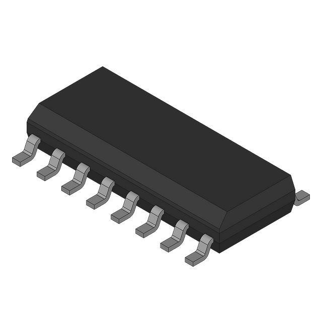
16 Lead SOIC and TSSOP Packages
Operating Temperature: –40°C to 85°C
APPLICATIONS
•
•
•
•
•
•
•
•
•
Gigabit Ethernet Redundant Transmission
Paths
Gigabit Interface Converters (GBICs)
Fibre Channel Redundant Transmission
Paths
HDTV Video Routing
Base Stations
Protection Switching for Serial Backplanes
Network Switches/Routers
Optical Networking Line Cards/Switches
Clock Distribution
DESCRIPTION
The SN65LVCP23 is a 2x2 LVPECL crosspoint
switch. The dual channels incorporate wide
common-mode (0 V to 4 V) receivers, allowing for
the receipt of LVDS, LVPECL, and CML signals. The
dual outputs are LVPECL drivers to provide
high-speed operation. The SN65LVCP23 provides a
single device supporting 2:2 buffering (repeating),
1:2 splitting, 2:1 multiplexing, 2x2 switching, and
LVDS/CML to LVPECL level translation on each
channel. The flexible operation of the SN65LVCP23
provides a single device to support the redundant
serial bus transmission needs (working and
protection switching cards) of fault-tolerant switch
systems found in optical networking, wireless
infrastructure, and data communications systems. TI
offers an additional gigabit repeater/translator in the
SN65LVDS101.
The SN65LVCP23 uses a fully differential data path
to ensure low-noise generation, fast switching times,
low pulse width distortion, and low jitter. Output
channel-to-channel skew is less than 10 ps (typ) and
50 ps (max) to ensure accurate alignment of outputs
in all applications. Both SOIC and TSSOP package
options are available.
OUTPUTS OPERATING SIMULTANEOUSLY
1.3 Gbps
223 -1 PRBS
OUTPUT 1
VCC = 3.3 V
|VID| = 200 mV, VIC = 1.2 V
Vertical Scale = 400 mV/div
OUTPUT 2
650 MHz
Horizontal Scale = 200 ps
Please be aware that an important notice concerning availability, standard warranty, and use in critical applications of Texas
Instruments semiconductor products and disclaimers thereto appears at the end of this data sheet.
PRODUCTION DATA information is current as of publication date.
Products conform to specifications per the terms of the Texas
Instruments standard warranty. Production processing does not
necessarily include testing of all parameters.
Copyright © 2002–2006, Texas Instruments Incorporated
�SN65LVCP23
www.ti.com
SLLS554E – NOVEMBER 2002 – REVISED MAY 2006
These devices have limited built-in ESD protection. The leads should be shorted together or the device placed in conductive foam
during storage or handling to prevent electrostatic damage to the MOS gates.
ORDERING INFORMATION
PART NUMBER (1)
SYMBOLIZATION
SOIC
SN65LVCP23D
LVCP23
TSSOP
SN65LVCP23PW
LVCP23
PACKAGE DESIGNATOR
(1)
Add the suffix R for taped and reeled carrier
PACKAGE DISSIPATION RATINGS
(1)
(2)
PACKAGE
CIRCUIT
BOARD MODEL
TA ≤ 25°C
POWER RATING
DERATING FACTOR (1)
ABOVE TA = 25°C
TA = 85°C
POWER RATING
SOIC (D)
High-K (2)
1361 mW
13.9 mW/°C
544 mW
TSSOP (PW)
High-K (2)
1074 mW
10.7 mW/°C
430 mW
This is the inverse of the junction-to-ambient thermal resistance when board-mounted and with no air flow.
In accordance with the High-K thermal metric definitions of EIA/JESD51-7.
THERMAL CHARACTERISTICS
PARAMETER
θJB
TEST CONDITIONS
Junction-to-board thermal resistance
θJC
Junction-to-case thermal resistance
PD
Device power dissipation
VALUE
UNITS
D
15.7
°C/W
PW
22.1
°C/W
D
26.1
°C/W
PW
17.3
°C/W
Typical
VCC = 3.3 V, TA = 25°C, 2 Gbps
165
mW
Maximum
VCC = 3.6 V, TA = 85°C, 2 Gbps
234
mW
FUNCTIONAL BLOCK DIAGRAM
OUT 0
OUT 1
EN 0
EN 1
SEL 1
SEL 0
0
1
0
IN 0
IN 1
2
Submit Documentation Feedback
1
�SN65LVCP23
www.ti.com
SLLS554E – NOVEMBER 2002 – REVISED MAY 2006
CIRCUIT FUNCTION TABLE
INPUTS (1)
OUTPUTS (1)
IN 0
IN 1
SEL 0
SEL1
EN 0
EN 1
OUT 0
OUT 1
X
X
X
X
L
L
L
L
>100 mV
X
L
L
H
L
H
L
100 mV
X
L
L
L
H
L
H
100 mV
X
L
H
H
L
H
L
100 mV
L
H
L
H
L
H
X
100 mV
H
H
H
L
H
L
X
100 mV
H
H
L
H
L
H
X
100 mV
H
L
H
L
H
L
X
100 mV
X
H
L
L
H
L
H
很抱歉,暂时无法提供与“SN65LVCP23D”相匹配的价格&库存,您可以联系我们找货
免费人工找货