SN65LVDS108
www.ti.com
SLLS399E – NOVEMBER 1999 – REVISED FEBRUARY 2005
8-PORT LVDS REPEATER
FEATURES
•
•
•
•
•
•
•
•
•
•
•
•
One Line Receiver and Eight Line Drivers
Configured as an 8-Port LVDS Repeater
Line Receiver and Line Drivers Meet or
Exceed the Requirements of ANSI EIA/TIA-644
Standard
Typical Data Signaling Rates to 400 Mbps or
Clock Frequencies to 400 MHz
Enabling Logic Allows Individual Control of
Each Driver Output, Plus All Outputs
Low-Voltage Differential Signaling With
Typical Output Voltage of 350 mV and a 100-Ω
Load
Electrically Compatible With LVDS, PECL,
LVPECL, LVTTL, LVCMOS, GTL, BTL, CTT,
SSTL, or HSTL Outputs With External
Termination Networks
Propagation Delay Times < 4.7 ns
Output Skew Less Than 300 ps and
Part-to-Part Skew Less Than 1.5 ns
Total Power Dissipation at 200 MHz Typically
Less Than 330 mW With 8 Channels Enabled
Driver Outputs or Receiver Input Equals High
Impedance When Disabled or With VCC < 1.5 V
Bus-Pin ESD Protection Exceeds 12 kV
Packaged in Thin Shrink Small-Outline
Package With 20-Mil Terminal Pitch
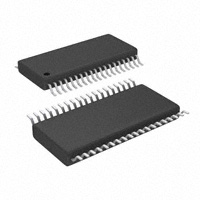
DBT PACKAGE
(TOP VIEW)
GND
VCC
GND
NC
ENM
ENA
ENB
ENC
END
A
B
ENE
ENF
ENG
ENH
NC
GND
VCC
GND
1
38
2
37
3
36
4
35
5
34
6
33
7
32
8
31
9
30
10
29
11
28
12
27
13
26
14
25
15
24
16
23
17
22
18
21
19
20
NC
AY
AZ
BY
BZ
CY
CZ
DY
DZ
EY
EZ
FY
FZ
GY
GZ
HY
HZ
NC
NC
NC – No internal connection
DESCRIPTION
The SN65LVDS108 is configured as one differential line receiver connected to eight differential line drivers.
Individual output enables are provided for each output and an additional enable is provided for all outputs.
The line receivers and line drivers implement the electrical characteristics of low-voltage differential signaling
(LVDS). LVDS, as specified in EIA/TIA-644, is a data signaling technique that offers low power, low noise
emission, high noise immunity, and high switching speeds. (Note: The ultimate rate and distance of data transfer
is dependent upon the attenuation characteristics of the media, the noise coupling to the environment, and other
system characteristics.)
The intended application of this device, and the LVDS signaling technique, is for point-to-point or
point-to-multipoint (distributed simplex) baseband data transmission on controlled impedance media of
approximately 100 Ω. The transmission media may be printed-circuit board traces, backplanes, or cables. The
large number of drivers integrated into the same silicon substrate, along with the low pulse skew of balanced
signaling, provides extremely precise timing alignment of the signals being repeated from the inputs. This is
particularly advantageous for implementing system clock or data distribution trees.
The SN65LVDS108 is characterized for operation from –40°C to 85°C.
Please be aware that an important notice concerning availability, standard warranty, and use in critical applications of Texas
Instruments semiconductor products and disclaimers thereto appears at the end of this data sheet.
PRODUCTION DATA information is current as of publication date.
Products conform to specifications per the terms of the Texas
Instruments standard warranty. Production processing does not
necessarily include testing of all parameters.
Copyright © 1999–2005, Texas Instruments Incorporated
�SN65LVDS108
www.ti.com
SLLS399E – NOVEMBER 1999 – REVISED FEBRUARY 2005
These devices have limited built-in ESD protection. The leads should be shorted together or the device
placed in conductive foam during storage or handling to prevent electrostatic damage to the MOS gates.
LOGIC DIAGRAM (POSITIVE LOGIC)
AY
ENA
AZ
ENM
BY
BZ
ENB
CY
CZ
ENC
DY
END
DZ
A
B
EY
ENE
EZ
FY
FZ
ENF
GY
GZ
ENG
HY
HZ
ENH
SELECTION GUIDE TO LVDS SPLITTER
The SN65LVDS108 is one member of a family of LVDS splitters and repeaters. A brief overview of the family is
provided in the following table.
LVDS SPLITTER AND REPEATER FAMILY
DEVICE
NUMBER OF INPUTS NUMBER OF OUTPUTS
PACKAGE
COMMENTS
SN65LVDS104
1 LVDS
4 LVDS
16-pin D
4-Port LVDS repeater
SN65LVDS105
1 LVTTL
4 LVDS
16-pin D
4-Port TTL-to-LVDS repeater
SN65LVDS108
1 LVDS
8 LVDS
38-pin DBT
8-Port LVDS repeater
SN65LVDS109
2 LVDS
8 LVDS
38-pin DBT
Dual 4-port LVDS repeater
SN65LVDS116
1 LVDS
16 LVDS
64-pin DGG
16-Port LVDS repeater
SN65LVDS117
2 LVDS
16 LVDS
64-pin DGG
Dual 8-port LVDS repeater
2
�SN65LVDS108
www.ti.com
SLLS399E – NOVEMBER 1999 – REVISED FEBRUARY 2005
FUNCTION TABLE
(1)
INPUTS
(1)
OUTPUTS
VID = VA – VB
ENM
ENx
xY
xZ
X
L
X
Z
Z
Z
X
X
L
Z
VID≥ 100 mV
H
H
H
L
–100 mV < VID < 100 mV
H
H
?
?
VID≤-100 mV
H
H
L
H
H = high level, L = low level, Z = high impedance, X = don't care, ? = indeterminate
EQUIVALENT INPUT AND OUTPUT SCHEMATIC DIAGRAMS
VCC
VCC
VCC
300 kΩ
(ENM Only)
300 kΩ
300 kΩ
Enable
Inputs
A Input
B Input
50 Ω
10 kΩ
5Ω
Y or Z
Output
7V
7V
300 kΩ
7V
7V
(ENx Only)
ABSOLUTE MAXIMUM RATINGS
over operating free-air temperature range (unless otherwise noted) (1)
UNIT
VCC
Supply voltage range (2)
Input voltage range
–0.5 V to 4 V
Enable inputs
–0.5 V to 6 V
A, B, Y or Z
–0.5 V to 4 V
Electrostatic discharge, A, B, Y, Z, and
GND (3)
Class 3, A:12 kV, B: 500 V
Continuous power dissipation
See Dissipation Rating Table
Storage temperature range
–65°C to 150°C
Lead temperature 1,6 mm (1/16 inch) from case for 10 seconds
(1)
(2)
(3)
260°C
Stresses beyond those listed under absolute maximum ratings may cause permanent damage to the device. These are stress ratings
only, and functional operation of the device at these or any other conditions beyond those indicated under recommended operating
conditions is not implied. Exposure to absolute-maximum-rated conditions for extended periods may affect device reliability.
All voltage values, except differential I/O bus voltages, are with respect to network ground terminal.
Tested in accordance with MIL-STD-883C Method 3015.7.
DISSIPATION RATING TABLE
(1)
PACKAGE
TA ≤ 25°C
POWER RATING
DERATING FACTOR (1)
ABOVE TA = 25°C
TA = 85°C
POWER RATING
DBT
1277 mW
10.2 mW/°C
644 mW
This is the inverse of the junction-to-ambient thermal resistance when board-mounted (low-k) with no air flow.
3
�SN65LVDS108
www.ti.com
SLLS399E – NOVEMBER 1999 – REVISED FEBRUARY 2005
RECOMMENDED OPERATING CONDITIONS
MIN
NOM
MAX
3.3
3.6
V
0.8
V
VCC
Supply voltage
3
VIH
High-level input voltage
2
VIL
Low-level input voltage
VI or VIC
Voltage at any bus terminal (separately or common-mode)
TA
Operating free-air temperature
UNIT
V
0
VCC– 0.8
V
40
85
°C
ELECTRICAL CHARACTERISTICS
over recommended operating conditions (unless otherwise noted)
PARAMETER
VITH+
Positive-going differential input voltage threshold
VITH-
Negative-going differential input voltage threshold
|VOD|
Differential output voltage magnitude
Change in differential output voltage magnitude be∆|VOD|
tween logic states
VOC(SS
TEST CONDITIONS
See Figure 1 and Table 1
RL = 100 Ω, VID = ±100 mV, See
Figure 1 and Figure 2
Steady-state common-mode output voltage
MIN
TYP (1)
MAX
100
100
247
340
UNIT
mV
454
50
50
1.125
1.375
50
50
mV
V
)
∆VOC(
SS)
VOC(PP
Change in steady-state common-mode output voltage
between logic states
See Figure 3
mV
Peak-to-peak common-mode output voltage
50
150
62
85
8
12
)
Enabled,
ICC
Supply current
II
Input current (A or B inputs)
II(OFF)
Power-off input current (A or B inputs)
VCC = 1.5 V,
IIH
High-level input current (enables)
IIL
Low-level input current (enables)
IOS
Short-circuit output current
IOZ
High-impedance output current
RL = 100 Ω
Disabled
VI = 0 V
2
VI = 2.4 V
VI = 2.4 V
µA
VIH = 2 V
±20
µA
VIL = 0.8 V
±10
µA
VOY or VOZ = 0 V
±24
VOD = 0 V
±12
VO = 0 V or VCC
VCC = 1.5 V,
CIN
Input capacitance (A or B inputs)
VI = 0.4 sin (4E6πt) + 0.5 V
Output capacitance (Y or Z outputs)
VI = 0.4 sin (4E6πt) + 0.5 V, Disabled
(1)
4
All typical values are at 25°C and with a 3.3-V supply.
µA
20
IO(OFF) Power-off output current
CO
20
1.2
mA
VO = 3.6 V
mA
±1
µA
±1
µA
5
9.4
pF
�SN65LVDS108
www.ti.com
SLLS399E – NOVEMBER 1999 – REVISED FEBRUARY 2005
SWITCHING CHARACTERISTICS
over recommended operating conditions (unless otherwise noted)
PARAMETER
TEST CONDITIONS
MIN
TYP (1)
MAX
tPLH
Propagation delay time, low-to-high-level output
1.6
2.8
4.5
tPHL
Propagation delay time, high-to-low-level output
1.6
2.8
4.5
0.3
0.8
1.2
0.3
0.8
1.2
150
500
tr
Differential output signal rise time
tf
Differential output signal fall time
tsk(p)
Pulse skew (|tPHL - tPLH|) (2)
RL = 100 Ω, CL = 10
pF, See Figure 4
skew (3)
tsk(o)
Output
tsk(pp)
Part-to-part skew (4)
tPZH
Propagation delay time, high-impedance-to-high-level output
tPZL
Propagation delay time, high-impedance-to-low-level output
tPHZ
Propagation delay time, high-level-to-high-impedance output
tPLZ
Propagation delay time, low-level-to-high-impedance output
(1)
(2)
(3)
(4)
UNIT
300
1.5
See Figure 5
5.7
15
7.7
15
3.2
15
3.2
15
ns
ns
ps
ns
ns
ns
All typical values are at 25°C and with a 3.3-V supply.
tsk(p) is the magnitude of the time difference between the tPLH and tPHL of any output of a single device.
tsk(o) is the magnitude of the time difference between the tPLH or tPHL measured at any two outputs.
tsk(pp) is the magnitude of the time difference in propagation delay times between any specified terminals of two devices when both
devices operate with the same supply voltages, at the same temperature, and have identical packages and test circuits.
PARAMETER MEASUREMENT INFORMATION
IOY
IIA
IIB
VID
A
Y
B
Z
IOZ
VOD
VOY
VOC
VIA
VOZ
VIB
(VOY + VOZ)/2
Figure 1. Voltage and Current Definitions
Table 1. Receiver Minimum and Maximum Input Threshold Test Voltages
APPLIED VOLTAGES
RESULTING DIFFERENTIAL
INPUT VOLTAGE
RESULTING COMMONMODE INPUT VOLTAGE
VIA
VIB
VID
VIC
1.25 V
1.15 V
100 mV
1.2 V
1.15 V
1.25 V
–100 mV
1.2 V
2.4 V
2.3 V
100 mV
2.35 V
2.3 V
2.4 V
–100 mV
2.35 V
0.1 V
0V
100 mV
0.05 V
0V
0.1 V
–100 mV
0.05 V
1.5 V
0.9 V
600 mV
1.2 V
0.9 V
1.5 V
–600 mV
1.2 V
2.4 V
1.8 V
600 mV
2.1 V
1.8 V
2.4 V
–600 mV
2.1 V
0.6 V
0V
600 mV
0.3 V
0V
0.6 V
–600 mV
0.3 V
5
�SN65LVDS108
www.ti.com
SLLS399E – NOVEMBER 1999 – REVISED FEBRUARY 2005
3.75 kΩ
Y
100 Ω
3.75 kΩ
VOD
Input
Z
±
0 V ≤ VTEST ≤ 2.4 V
Figure 2. VOD Test Circuit
49.9 Ω ± 1% (2 Places)
Y
Input
Input
VI
1.4 V
VI
1V
Z
50 pF
VOC(PP)
VOC(SS)
VOC
VO
A.
All input pulses are supplied by a generator having the following characteristics: tr or tf ≤ 1 ns, pulse repetition rate
(PRR) = 0.5 Mpps, pulsewidth = 500 ±10 ns. CL includes instrumentation and fixture capacitance within 0,06 mm of
the D.U.T. The measurement of VOC(PP) is made on test equipment with a –3 dB bandwidth of at least 300 MHz.
Figure 3. Test Circuit and Definitions for the Driver Common-Mode Output Voltage
A
Y
B
Z
Input
1.4 V
1.2 V
1V
VIB
Input
VIA
tPLH
VOD
tPHL
100 Ω ± 1 %
100%
80%
VOD(H)
Output
CL = 10 pF
(2 Places)
0V
VOD(L)
20%
0%
tf
A.
tr
All input pulses are supplied by a generator having the following characteristics: tr or tf≤ 1 ns, pulse repetition rate
(PRR) = 50 Mpps, pulsewidth = 10 ±0.2 ns . CL includes instrumentation and fixture capacitance within 0,06 mm of
the D.U.T.
Figure 4. Test Circuit, Timing, and Voltage Definitions for the Differential Output Signal
6
�SN65LVDS108
www.ti.com
SLLS399E – NOVEMBER 1999 – REVISED FEBRUARY 2005
Y
1 V or 1.4 V
49.9 Ω ± 1% (2 Places)
Z
1.4 V or 1 V
1.2 V
CL = 10 pF
ENM (2 Places)
ENx
Inputs
VOY
2V
1.4 V
0.8 V
Input
tPZH
tPHZ
VOY
or
VOZ
100%, ≅ 1.4 V
50%
0%, 1.2 V
tPZL
VOZ
or
VOY
A.
VOZ
tPLZ
100%, 1.2 V
50%
0%, ≅ 1 V
All input pulses are supplied by a generator having the following characteristics: tr or tf ≤ 1 ns, pulse repetition rate
(PRR) = 0.5 Mpps, pulsewidth = 500 ±10 ns . CL includes instrumentation and fixture capacitance within 0,06 mm of
the D.U.T.
Figure 5. Enable and Disable Time Circuit and Definitions
7
�SN65LVDS108
www.ti.com
SLLS399E – NOVEMBER 1999 – REVISED FEBRUARY 2005
TYPICAL CHARACTERISTICS
SUPPLY CURRENT
vs
SWITCHING FREQUENCY
LOW-TO-HIGH PROPAGATION DELAY TIME
vs
FREE-AIR TEMPERATURE
t PLH − Low-To-High Propagation Delay Time − ns
140
I CC − Supply Current − mA
120
VCC = 3.6 V
100
VCC = 3 V
80
VCC = 3.3 V
60
40
20
All Outputs Loaded
and Enabled
0
0
50
100
150
200
250
300
350
3.8
3.7
3.6
3.5
VCC = 3.3 V
3.4
VCC = 3 V
VCC = 3.6 V
3.3
3.2
3.1
−50
−25
0
25
50
75
100
TA − Free−Air Temperature − °C
f − Frequency − MHz
Figure 6.
Figure 7.
t PHL − High-To-Low Propagation Delay Time − ns
HIGH-TO-LOW PROPAGATION DELAY TIME
vs
FREE-AIR TEMPERATURE
3.7
3.6
3.5
3.4
3.3
VCC = 3.3 V
VCC = 3.6 V
VCC = 3 V
3.2
3.1
3.0
2.9
−50
−25
0
25
50
75
100
TA − Free−Air Temperature − °C
Figure 8.
8
Figure 9. Typical Differential Eye Pattern at 400 Mbps
�SN65LVDS108
www.ti.com
SLLS399E – NOVEMBER 1999 – REVISED FEBRUARY 2005
TYPICAL CHARACTERISTICS (continued)
P-P EYE-PATTERN JITTER
vs
PRBS SIGNALING RATE
700
TA = 25�C
Peak-to-Peak Jitter − ps
600
VCC = 3.6 V
500
VCC = 3 V
400
300
200
100
00
100
200
300
400
500
Signaling Rate − Mbps
NOTES: Input: 215 PRBS with peak-to-peak jitter < 100 ps at 100 Mbps, all outputs enabled and loaded with differential
100-Ω loads, worst-case output, supply decoupled with 0.1-µF and 0.001-µF ceramic 0603-style capacitors 1 cm from
the device.
Figure 10.
P-P PERIOD JITTER
vs
CLOCK FREQUENCY
50
45
TA = 25�C
Peak-to-Peak Jitter − ps
40
VCC = 3.6 V
35
30
VCC = 3 V
25
20
15
10
5
0
0
100
200
300
400
500
Clock Frequency − MHz
NOTES: Input: 50% duty cycle square wave with period jitter < 9 ps at 100 MHz, all outputs enabled and loaded with
differential 100-Ω loads,worst-case output, supply decoupled with 0.1-µF and 0.001- µF ceramic 0603-style capacitors
1 cm from the device.
Figure 11.
9
�SN65LVDS108
www.ti.com
SLLS399E – NOVEMBER 1999 – REVISED FEBRUARY 2005
APPLICATION INFORMATION
FAIL SAFE
A common problem with differential signaling applications is how the system responds when no differential
voltage is present on the signal pair. The LVDS receiver is like most differential line receivers, in that its output
logic state can be indeterminate when the differential input voltage is between –100 mV and 100 mV and within
its recommended input common-mode voltage range. Hovever, TI LVDS receivers handles the open-input circuit
situation differently.
Open-circuit means that there is little or no input current to the receiver from the data line itself. This could be
when the driver is in a high-impedance state or the cable is disconnected. When this occurs, the LVDS receiver
pulls each line of the signal pair to near VCC through 300-kΩ resistors as shown in Figure 12. The fail-safe
feature uses an AND gate with input voltage thresholds at about 2.3 V to detect this condition and force the
output to a high-level regardless of the differential input voltage.
VCC
300 kΩ
300 kΩ
A
Rt = 100 Ω (Typ)
Y
B
VIT ≈ 2.3 V
Figure 12. Open-Circuit Fail Safe of the LVDS Receiver
It is only under these conditions that the output of the receiver will be valid with less than a 100 mV differential
input voltage magnitude. The presence of the termination resistor, Rt, does not affect the fail-safe function as
long as it is connected as shown in Figure 12. Other termination circuits may allow a dc current to ground that
could defeat the pullup currents from the receiver and the fail-safe feature.
CLOCK DISTRIBUTION
The SN65LVDS108 device solves several problems common to the distribution of timing critical clock and data
signals. These problems include:
• Excessive skew between the signal paths
• Noise pickup over long signaling paths
• High power consumption
• Control of which signal paths are enabled or disabled
• Elimination of radiation from unterminated lines
Buffering and splitting the signal on the same silicon die minimizes corruption of the timing relation between the
copies of the signal. Buffering and splitting the signal in separate devices will introduce considerably higher levels
of uncontrolled timing skew between the signals. Higher speed operation and more timing tolerance for other
components of the system is enabled by the tighter system timing budgets provided by the single die
implementations of the SN65LVDS108.
The use of LVDS signaling technology for both the inputs and the outputs provides superior common-mode and
noise tolerance compared to single-ended I/O technologies. This is particularly important because the signals
that are being distributed must be transmitted over longer distances, and at higher rates, than can be
accommodated with single-ended I/Os. In addition, LVDS consumes considerably less power than other
high-performance differential signaling schemes.
10
�SN65LVDS108
www.ti.com
SLLS399E – NOVEMBER 1999 – REVISED FEBRUARY 2005
APPLICATION INFORMATION (continued)
The enable inputs provided for each output may be used to turn on or off any of the paths. This function is
required to prevent radiation of signals from the unterminated signal lines on open connectors when boards or
devices are being swapped in the end equipment. The individual channel enables are also required if redundant
paths are being utilized for reliability reasons.
The following diagram shows how an input signal is being identically repeated out two of the available outputs. A
third output is shown in the disabled state.
n-PORT REPEATER
DESTINATION
EQUIPMENT/
BOARD #1
SOURCE
EQUIPMENT/
BOARD
Output Pair Disabled
DESTINATION
EQUIPMENT/
BOARD #2
DESTINATION
EQUIPMENT/
BOARD #n
Figure 13. LVDS Repeating Splitter Application Example Showing Individual Path Control
INPUT LEVEL TRANSLATION
An LVDS receiver can be used to receive various other types of logic signals. Figure 14 through Figure 22 show
the termination circuits for SSTL, HSTL, CTT, GTL, BTL, LVPECL, PECL, CMOS, and TTL.
VDD
25 Ω
50 Ω
A
1/2 VDD
50
Ω
0.1 µF
B
LVDS Receiver
Figure 14. Stub-Series Terminated (SSTL) or High-Speed Transceiver Logic (HSTL)
11
�SN65LVDS108
www.ti.com
SLLS399E – NOVEMBER 1999 – REVISED FEBRUARY 2005
APPLICATION INFORMATION (continued)
VDD
50 Ω
A
50 Ω
B
1.35 V < VTT < 1.65 V
0.1 µF
LVDS Receiver
Figure 15. Center-Tap Termination (CTT)
1.14 V < VTT < 1.26 V
VDD
50 Ω
1 kΩ
50 Ω
A
B
2 kΩ
0.1 µF
LVDS Receiver
Figure 16. Gunning Transceiver Logic (GTL)
Z0
Z0
A
B
1.47 V < VTT < 1.62 V
0.1 µF
Figure 17. Backplane Transceiver Logic (BTL)
12
LVDS Receiver
�SN65LVDS108
www.ti.com
SLLS399E – NOVEMBER 1999 – REVISED FEBRUARY 2005
APPLICATION INFORMATION (continued)
3.3 V
3.3 V
50 Ω
120 Ω
120 Ω
33 Ω
ECL
A
50 Ω
33 Ω
B
51 Ω
51 Ω
LVDS Receiver
Figure 18. Low-Voltage Positive Emitter-Coupled Logic (LVPECL)
5V
5V
50 Ω
82 Ω
82 Ω
100 Ω
ECL
A
50 Ω
100 Ω
33 Ω
B
33 Ω
LVDS Receiver
Figure 19. Positive Emitter-Coupled Logic (PECL)
13
�SN65LVDS108
www.ti.com
SLLS399E – NOVEMBER 1999 – REVISED FEBRUARY 2005
APPLICATION INFORMATION (continued)
3.3 V
3.3 V
7.5 kΩ
A
B
7.5 kΩ
0.1 µF
LVDS Receiver
Figure 20. 3.3-V CMOS
5V
5V
10 kΩ
560 Ω
A
B
560 Ω
3.32 kΩ
0.1 µF
LVDS Receiver
Figure 21. 5-V CMOS
5V
5V
10 kΩ
470 Ω
A
B
3.3 V
4.02 kΩ
Figure 22. TTL
14
0.1 µF
LVDS Receiver
�PACKAGE OPTION ADDENDUM
www.ti.com
14-Oct-2022
PACKAGING INFORMATION
Orderable Device
Status
(1)
Package Type Package Pins Package
Drawing
Qty
Eco Plan
(2)
Lead finish/
Ball material
MSL Peak Temp
Op Temp (°C)
Device Marking
(3)
Samples
(4/5)
(6)
SN65LVDS108DBT
ACTIVE
TSSOP
DBT
38
50
RoHS & Green
NIPDAU
Level-2-260C-1 YEAR
-40 to 85
LVDS108
Samples
SN65LVDS108DBTG4
ACTIVE
TSSOP
DBT
38
50
RoHS & Green
NIPDAU
Level-2-260C-1 YEAR
-40 to 85
LVDS108
Samples
SN65LVDS108DBTR
ACTIVE
TSSOP
DBT
38
2000
RoHS & Green
NIPDAU
Level-2-260C-1 YEAR
-40 to 85
LVDS108
Samples
(1)
The marketing status values are defined as follows:
ACTIVE: Product device recommended for new designs.
LIFEBUY: TI has announced that the device will be discontinued, and a lifetime-buy period is in effect.
NRND: Not recommended for new designs. Device is in production to support existing customers, but TI does not recommend using this part in a new design.
PREVIEW: Device has been announced but is not in production. Samples may or may not be available.
OBSOLETE: TI has discontinued the production of the device.
(2)
RoHS: TI defines "RoHS" to mean semiconductor products that are compliant with the current EU RoHS requirements for all 10 RoHS substances, including the requirement that RoHS substance
do not exceed 0.1% by weight in homogeneous materials. Where designed to be soldered at high temperatures, "RoHS" products are suitable for use in specified lead-free processes. TI may
reference these types of products as "Pb-Free".
RoHS Exempt: TI defines "RoHS Exempt" to mean products that contain lead but are compliant with EU RoHS pursuant to a specific EU RoHS exemption.
Green: TI defines "Green" to mean the content of Chlorine (Cl) and Bromine (Br) based flame retardants meet JS709B low halogen requirements of