SN74AVC16334
16-BIT UNIVERSAL BUS DRIVER
WITH 3-STATE OUTPUTS
www.ti.com
SCES154I – DECEMBER 1998 – REVISED MAY 2005
•
FEATURES
•
•
•
Member of the Texas Instruments Widebus™
Family
DOC™ (Dynamic Output Control) Circuit
Dynamically Changes Output Impedance,
Resulting in Noise Reduction Without Speed
Degradation
Dynamic Drive Capability Is Equivalent to
Standard Outputs With IOH and IOL of ±24 mA
at 2.5-V VCC
Overvoltage-Tolerant Inputs/Outputs Allow
Mixed-Voltage-Mode Data Communications
Ioff Supports Partial-Power-Down Mode
Operation
ESD Protection Exceeds JESD 22
– 2000-V Human-Body Model (A114-A)
– 200-V Machine Model (A115-A)
Latch-Up Performance Exceeds 100 mA Per
JESD 78, Class II
•
•
•
DESCRIPTION
A Dynamic Output Control (DOC™) circuit is implemented, which, during the transition, initially lowers the output
impedance to effectively drive the load and, subsequently, raises the impedance to reduce noise. Figure 1 shows
typical VOL vs IOL and VOH vs IOH curves to illustrate the output impedance and drive capability of the circuit. At
the beginning of the signal transition, the DOC circuit provides a maximum dynamic drive that is equivalent to a
high-drive standard-output device. For more information, refer to the TI application reports, AVC Logic Family
Technology and Applications, literature number SCEA006, and Dynamic Output Control (DOC™) Circuitry
Technology and Applications, literature number SCEA009.
3.2
TA = 25°C
Process = Nominal
- Output Voltage - V
2.8
2.4
VCC = 3.3 V
2.0
1.6
VCC = 2.5 V
1.2
OH
VCC = 1.8 V
0.8
V
VOL - Output Voltage - V
2.8
TA = 25°C
Process = Nominal
2.4
2.0
1.6
1.2
0.8
VCC = 3.3 V
0.4
0.4
0
17
34
51
68
85 102 119
IOL - Output Current - mA
136
153
170
VCC = 2.5 V
VCC = 1.8 V
-160 -144 -128 -112 -96 -80 -64 -48
IOH - Output Current - mA
-32
-16
0
Figure 1. Output Voltage vs Output Current
This 16-bit universal bus driver is operational at 1.2-V to 3.6-V VCC, but is designed specifically for 1.65-V to
3.6-V VCC operation.
Data flow from A to Y is controlled by the output-enable (OE) input. The device operates in the transparent mode
when the latch-enable (LE) input is low. When LE is high, the A data is latched if the clock (CLK) input is held at
a high or low logic level. If LE is high, the A data is stored in the latch/flip-flop on the low-to-high transition of
CLK. When OE is high, the outputs are in the high-impedance state.
To ensure the high-impedance state during power up or power down, OE should be tied to VCC through a pullup
resistor; the minimum value of the resistor is determined by the current-sinking capability of the driver.
This device is fully specified for partial-power-down applications using Ioff. The Ioff circuitry disables the outputs,
preventing damaging current backflow through the device when it is powered down.
Please be aware that an important notice concerning availability, standard warranty, and use in critical applications of Texas
Instruments semiconductor products and disclaimers thereto appears at the end of this data sheet.
Widebus, DOC are trademarks of Texas Instruments.
PRODUCTION DATA information is current as of publication date.
Products conform to specifications per the terms of the Texas
Instruments standard warranty. Production processing does not
necessarily include testing of all parameters.
Copyright © 1998–2005, Texas Instruments Incorporated
�SN74AVC16334
16-BIT UNIVERSAL BUS DRIVER
WITH 3-STATE OUTPUTS
www.ti.com
SCES154I – DECEMBER 1998 – REVISED MAY 2005
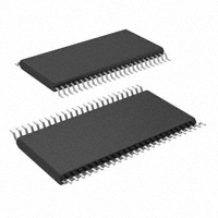
TERMINAL ASSIGNMENTS
DGG OR DGV PACKAGE
(TOP VIEW)
OE
Y1
Y2
GND
Y3
Y4
VCC
Y5
Y6
GND
Y7
Y8
Y9
Y10
GND
Y11
Y12
VCC
Y13
Y14
GND
Y15
Y16
NC
1
48
2
47
3
46
4
45
5
44
6
43
7
42
8
41
9
40
10
39
11
38
12
37
13
36
14
35
15
34
16
33
17
32
18
31
19
30
20
29
21
28
22
27
23
26
24
25
CLK
A1
A2
GND
A3
A4
VCC
A5
A6
GND
A7
A8
A9
A10
GND
A11
A12
VCC
A13
A14
GND
A15
A16
LE
NC - No internal connection
ORDERING INFORMATION
PACKAGE (1)
TA
–40°C to 85°C
(1)
2
ORDERABLE PART NUMBER
TOP-SIDE MARKING
TSSOP – DGG
Tape and reel
SN74AVC16334DGGR
AVC16334
TVSOP – DGV
Tape and reel
SN74AVC16334DGVR
CVA334
Package drawings, standard packing quantities, thermal data, symbolization, and PCB design guidelines are available at
www.ti.com/sc/package.
�SN74AVC16334
16-BIT UNIVERSAL BUS DRIVER
WITH 3-STATE OUTPUTS
www.ti.com
SCES154I – DECEMBER 1998 – REVISED MAY 2005
FUNCTION TABLE
(EACH UNIVERSAL BUS DRIVER)
INPUTS
(1)
OE
LE
CLK
A
OUTPUT
Y
H
X
X
X
Z
L
L
X
L
L
L
L
X
H
H
L
H
↑
L
L
L
H
↑
H
H
L
H
L or H
X
Y0 (1)
Output level before the indicated steady-state input conditions were
established
LOGIC DIAGRAM (POSITIVE LOGIC)
1
OE
48
CLK
LE
25
47
A1
1D
2
C1
Y1
CLK
To 15 Other Channels
Absolute Maximum Ratings (1)
over operating free-air temperature range (unless otherwise noted)
MIN
MAX
VCC
Supply voltage range
–0.5
4.6
V
VI
Input voltage range (2)
–0.5
4.6
V
–0.5
4.6
V
–0.5
VCC + 0.5
state (2)
UNIT
VO
Voltage range applied to any output in the high-impedance or power-off
VO
Voltage range applied to any output in the high or low state (2) (3)
IIK
Input clamp current
VI < 0
–50
mA
IOK
Output clamp current
VO < 0
–50
mA
IO
Continuous output current
±50
mA
±100
mA
Continuous current through each VCC or GND
θJA
Package thermal impedance (4)
Tstg
Storage temperature range
(1)
(2)
(3)
(4)
DGG package
70
DGV package
58
–65
150
V
°C/W
°C
Stresses beyond those listed under "absolute maximum ratings" may cause permanent damage to the device. These are stress ratings
only, and functional operation of the device at these or any other conditions beyond those indicated under "recommended operating
conditions" is not implied. Exposure to absolute-maximum-rated conditions for extended periods may affect device reliability.
The input and output negative-voltage ratings may be exceeded if the input and output current ratings are observed.
The output positive-voltage rating may be exceeded up to 4.6 V maximum if the output current rating is observed.
The package thermal impedance is calculated in accordance with JESD 51-7.
3
�SN74AVC16334
16-BIT UNIVERSAL BUS DRIVER
WITH 3-STATE OUTPUTS
www.ti.com
SCES154I – DECEMBER 1998 – REVISED MAY 2005
Recommended Operating Conditions (1)
VCC
Supply voltage
MIN
MAX
Operating
1.4
3.6
Data retention only
1.2
VCC = 1.2 V
VIH
High-level input voltage
0.65 × VCC
VCC = 1.65 V to 1.95 V
0.65 × VCC
VCC = 3 V to 3.6 V
Low-level input voltage
2
GND
VCC = 1.4 V to 1.6 V
0.35 × VCC
VCC = 1.65 V to 1.95 V
0.35 × VCC
VCC = 2.3 V to 2.7 V
Input voltage
VO
Output voltage
IOHS
Static high-level output current (2)
0.8
0
3.6
Active state
0
VCC
3-state
0
3.6
VCC = 1.4 V to 1.6 V
–2
VCC = 1.65 V to 1.95 V
–4
VCC = 2.3 V to 2.7 V
–8
VCC = 3 V to 3.6 V
Static low-level output current (2)
IOLS
Input transition rise or fall rate
TA
Operating free-air temperature
(1)
(2)
4
V
V
mA
–12
VCC = 1.4 V to 1.6 V
2
VCC = 1.65 V to 1.95 V
4
VCC = 2.3 V to 2.7 V
8
VCC = 3 V to 3.6 V
∆t/∆v
V
0.7
VCC = 3 V to 3.6 V
VI
V
1.7
VCC = 1.2 V
VIL
V
VCC
VCC = 1.4 V to 1.6 V
VCC = 2.3 V to 2.7 V
UNIT
mA
12
VCC = 1.4 V to 3.6 V
–40
5
ns/V
85
°C
All unused inputs of the device must be held at VCC or GND to ensure proper device operation. Refer to the TI application report,
Implications of Slow or Floating CMOS Inputs, literature number SCBA004.
Dynamic drive capability is equivalent to standard outputs with IOH and IOL of ±24 mA at 3.3-V VCC. See Figure 1 for VOL vs IOL and VOH
vs IOH characteristics. Refer to the TI application reports, AVC Logic Family Technology and Applications, literature number SCEA006,
and Dynamic Output Control (DOC™) Circuitry Technology and Applications, literature number SCEA009.
�SN74AVC16334
16-BIT UNIVERSAL BUS DRIVER
WITH 3-STATE OUTPUTS
www.ti.com
SCES154I – DECEMBER 1998 – REVISED MAY 2005
Electrical Characteristics
over recommended operating free-air temperature range (unless otherwise noted)
PARAMETER
TEST CONDITIONS
VCC
IOHS = –100 µA
VOH
1.4 V to 3.6 V
TYP (1)
MAX
UNIT
VCC – 0.2
IOHS = –2 mA,
VIH = 0.91 V
1.4 V
IOHS = –4 mA,
VIH = 1.07 V
1.65 V
1.2
IOHS = –8 mA,
VIH = 1.7 V
2.3 V
1.75
IOHS = –12 mA,
VIH = 2 V
3V
2.3
IOLS = 100 µA
VOL
MIN
1.05
V
1.4 V to 3.6 V
0.2
IOLS = 2 mA,
VIL = 0.49 V
1.4 V
0.4
IOLS = 4 mA,
VIL = 0.57 V
1.65 V
0.45
IOLS = 8 mA,
VIL = 0.7 V
2.3 V
0.55
IOLS = 12 mA,
VIL = 0.8 V
3V
0.7
V
II
VI = VCC or GND
3.6 V
±2.5
µA
Ioff
VI or VO = 3.6 V
0
±10
µA
IOZ
VO = VCC or GND
3.6 V
±10
µA
ICC
VI = VCC or GND,
3.6 V
40
µA
CLK input
Ci
Co
(1)
IO = 0
VI = VCC or GND
Control inputs
VI = VCC or GND
Data inputs
VI = VCC or GND
Outputs
VO = VCC or GND
2.5 V
4
3.3 V
4
2.5 V
4
3.3 V
4
2.5 V
2.5
3.3 V
2.5
2.5 V
6.5
3.3 V
6.5
pF
pF
Typical values are measured at TA = 25°C.
Timing Requirements
over recommended operating free-air temperature range (unless otherwise noted) (see Figure 2 through Figure 5)
VCC = 1.2 V
MIN
fclock
Clock frequency
tw
Pulse
duration
tsu
Setup
time
MAX
VCC = 1.5 V
± 0.1 V
MIN
MAX
VCC = 1.8 V
± 0.15 V
MIN
MAX
VCC = 2.5 V
± 0.2 V
MIN
150
MAX
VCC = 3.3 V
± 0.3 V
MIN
150
150
LE low
3.3
3.3
3.3
CLK high or low
3.3
3.3
3.3
Data before CLK↑
Data
before LE↑
UNIT
MAX
MHz
ns
1
0.8
0.7
0.7
0.7
CLK high
1.5
1.4
0.9
0.9
0.9
CLK low
2.7
1.6
1.2
1
1
1.3
1.1
0.9
0.8
0.7
ns
CLK high
2.2
1.9
1.7
1.5
1.5
ns
CLK low
2.4
1.8
1.6
1.4
1.3
ns
th
Hold
time
Data after CLK↑
th
Hold
time
Data
after LE↑
ns
5
�SN74AVC16334
16-BIT UNIVERSAL BUS DRIVER
WITH 3-STATE OUTPUTS
www.ti.com
SCES154I – DECEMBER 1998 – REVISED MAY 2005
Switching Characteristics
over recommended operating free-air temperature range (unless otherwise noted) (see Figure 2 through Figure 5)
FROM
(INPUT)
PARAMETER
TO
(OUTPUT)
VCC = 1.2 V
VCC = 1.5 V
± 0.1 V
VCC = 1.8 V
± 0.15 V
MAX
MIN
MAX
5.3
1.2
6.2
1.5
4.9
1
3.2
0.9
2.5
Y
7
2.2
9.7
1.8
7.5
1.5
4.9
0.8
4
150
tpd
LE
CLK
150
MIN
UNIT
MIN
A
MAX
VCC = 3.3 V
± 0.3 V
TYP
fmax
MIN
VCC = 2.5 V
± 0.2 V
MAX
150
MHz
ns
6
1.9
7.8
1.6
6
1.1
3.7
1
3.1
ten
OE
Y
7.9
2.4
10.2
1.6
8.8
1.5
6.7
1
6.2
ns
tdis
OE
Y
7.7
2.1
10.3
1.5
8.4
1.2
5.3
1
5.3
ns
Switching Characteristics (1)
TA = 0°C to 85°C, CL = 0 pF
FROM
(INPUT)
PARAMETER
A
tpd
(1)
VCC = 3.3 V
± 0.15 V
TO
(OUTPUT)
Y
CLK
MIN
MAX
0.6
1.3
0.7
1.5
UNIT
ns
Texas Instruments SPICE simulation data
Operating Characteristics
TA = 25°C
PARAMETER
Cpd
6
Power dissipation
capacitance
TEST CONDITIONS
Outputs enabled
Outputs disabled
CL = 0,
f = 10 MHz
VCC = 1.8 V
VCC = 2.5 V
VCC = 3.3 V
TYP
TYP
TYP
45
48
52
23
25
28
UNIT
pF
�SN74AVC16334
16-BIT UNIVERSAL BUS DRIVER
WITH 3-STATE OUTPUTS
www.ti.com
SCES154I – DECEMBER 1998 – REVISED MAY 2005
PARAMETER MEASUREMENT INFORMATION
VCC = 1.2 V AND 1.5 V ± 0.1 V
2 × VCC
2 kΩ
From Output
Under Test
S1
Open
TEST
tpd
tPLZ/tPZL
tPHZ/tPZH
GND
CL = 15 pF
(see Note A)
2 kΩ
S1
Open
2 × VCC
GND
LOAD CIRCUIT
tw
VCC
Timing
Input
VCC/2
VCC/2
VCC/2
0V
VOLTAGE WAVEFORMS
SETUP AND HOLD TIMES
VCC/2
VCC/2
0V
tPLH
Output
Control
(low-level
enabling)
VCC/2
VOL
VOLTAGE WAVEFORMS
PROPAGATION DELAY TIMES
tPLZ
VCC
VCC/2
tPZH
VOH
VCC/2
0V
Output
Waveform 1
S1 at 2 × VCC
(see Note B)
tPHL
VCC/2
VCC
VCC/2
tPZL
VCC
Input
VOLTAGE WAVEFORMS
PULSE DURATION
th
VCC
Data
Input
VCC/2
0V
0V
tsu
Output
VCC
VCC/2
Input
Output
Waveform 2
S1 at GND
(see Note B)
VOL + 0.1 V
VOL
tPHZ
VOH
VCC/2
VOH − 0.1 V
0V
VOLTAGE WAVEFORMS
ENABLE AND DISABLE TIMES
NOTES: A. CL includes probe and jig capacitance.
B. Waveform 1 is for an output with internal conditions such that the output is low, except when disabled by the output control.
Waveform 2 is for an output with internal conditions such that the output is high, except when disabled by the output control.
C. All input pulses are supplied by generators having the following characteristics: PRR ≤ 10 MHz, ZO = 50 Ω, tr ≤ 2 ns, tf ≤ 2 ns.
D. The outputs are measured one at a time, with one transition per measurement.
E. tPLZ and tPHZ are the same as tdis.
F. tPZL and tPZH are the same as ten.
G. tPLH and tPHL are the same as tpd.
Figure 2. Load Circuit and Voltage Waveforms
7
�SN74AVC16334
16-BIT UNIVERSAL BUS DRIVER
WITH 3-STATE OUTPUTS
www.ti.com
SCES154I – DECEMBER 1998 – REVISED MAY 2005
PARAMETER MEASUREMENT INFORMATION
VCC = 1.8 V ± 0.15 V
2 × VCC
1 kΩ
From Output
Under Test
S1
Open
GND
CL = 30 pF
(see Note A)
1 kΩ
TEST
S1
tpd
tPLZ/tPZL
tPHZ/tPZH
Open
2 × VCC
GND
LOAD CIRCUIT
tw
VCC
Timing
Input
VCC/2
VCC/2
VCC/2
0V
VOLTAGE WAVEFORMS
SETUP AND HOLD TIMES
VCC/2
VCC/2
0V
tPLH
Output
Control
(low-level
enabling)
VCC/2
VOL
VOLTAGE WAVEFORMS
PROPAGATION DELAY TIMES
tPLZ
VCC
VCC/2
tPZH
VOH
VCC/2
0V
Output
Waveform 1
S1 at 2 × VCC
(see Note B)
tPHL
VCC/2
VCC
VCC/2
tPZL
VCC
Input
VOLTAGE WAVEFORMS
PULSE DURATION
th
VCC
Data
Input
VCC/2
0V
0V
tsu
Output
VCC
VCC/2
Input
Output
Waveform 2
S1 at GND
(see Note B)
VOL + 0.15 V
VOL
tPHZ
VCC/2
VOH
VOH − 0.15 V
0V
VOLTAGE WAVEFORMS
ENABLE AND DISABLE TIMES
NOTES: A. CL includes probe and jig capacitance.
B. Waveform 1 is for an output with internal conditions such that the output is low, except when disabled by the output control.
Waveform 2 is for an output with internal conditions such that the output is high, except when disabled by the output control.
C. All input pulses are supplied by generators having the following characteristics: PRR ≤ 10 MHz, ZO = 50 Ω, tr ≤ 2 ns, tf ≤ 2 ns.
D. The outputs are measured one at a time, with one transition per measurement.
E. tPLZ and tPHZ are the same as tdis.
F. tPZL and tPZH are the same as ten.
G. tPLH and tPHL are the same as tpd.
Figure 3. Load Circuit and Voltage Waveforms
8
�SN74AVC16334
16-BIT UNIVERSAL BUS DRIVER
WITH 3-STATE OUTPUTS
www.ti.com
SCES154I – DECEMBER 1998 – REVISED MAY 2005
PARAMETER MEASUREMENT INFORMATION
VCC = 2.5 V ± 0.2 V
2 × VCC
500 Ω
From Output
Under Test
S1
Open
GND
CL = 30 pF
(see Note A)
500 Ω
TEST
S1
tpd
tPLZ/tPZL
tPHZ/tPZH
Open
2 × VCC
GND
LOAD CIRCUIT
tw
VCC
Timing
Input
VCC/2
VCC/2
VCC/2
0V
VOLTAGE WAVEFORMS
SETUP AND HOLD TIMES
VCC/2
VCC/2
0V
tPLH
Output
Control
(low-level
enabling)
VCC/2
VOL
VOLTAGE WAVEFORMS
PROPAGATION DELAY TIMES
tPLZ
VCC
VCC/2
tPZH
VOH
VCC/2
0V
Output
Waveform 1
S1 at 2 × VCC
(see Note B)
tPHL
VCC/2
VCC
VCC/2
tPZL
VCC
Input
VOLTAGE WAVEFORMS
PULSE DURATION
th
VCC
Data
Input
VCC/2
0V
0V
tsu
Output
VCC
VCC/2
Input
Output
Waveform 2
S1 at GND
(see Note B)
VOL + 0.15 V
VOL
tPHZ
VCC/2
VOH
VOH − 0.15 V
0V
VOLTAGE WAVEFORMS
ENABLE AND DISABLE TIMES
NOTES: A. CL includes probe and jig capacitance.
B. Waveform 1 is for an output with internal conditions such that the output is low, except when disabled by the output control.
Waveform 2 is for an output with internal conditions such that the output is high, except when disabled by the output control.
C. All input pulses are supplied by generators having the following characteristics: PRR ≤ 10 MHz, ZO = 50 Ω, tr ≤ 2 ns, tf ≤ 2 ns.
D. The outputs are measured one at a time, with one transition per measurement.
E. tPLZ and tPHZ are the same as tdis.
F. tPZL and tPZH are the same as ten.
G. tPLH and tPHL are the same as tpd.
Figure 4. Load Circuit and Voltage Waveforms
9
�SN74AVC16334
16-BIT UNIVERSAL BUS DRIVER
WITH 3-STATE OUTPUTS
www.ti.com
SCES154I – DECEMBER 1998 – REVISED MAY 2005
PARAMETER MEASUREMENT INFORMATION
VCC = 3.3 V ± 0.3 V
2 × VCC
500 Ω
From Output
Under Test
S1
Open
GND
CL = 30 pF
(see Note A)
500 Ω
TEST
S1
tpd
tPLZ/tPZL
tPHZ/tPZH
Open
2 × VCC
GND
tw
LOAD CIRCUIT
VCC
VCC
Timing
Input
VCC/2
Input
VCC/2
0V
VCC/2
0V
tsu
VOLTAGE WAVEFORMS
PULSE DURATION
th
VCC
Data
Input
VCC/2
VCC/2
0V
VOLTAGE WAVEFORMS
SETUP AND HOLD TIMES
Output
Control
(low-level
enabling)
VCC
VCC/2
VCC/2
0V
tPZL
VCC
Input
VCC/2
VCC/2
0V
tPLH
VCC/2
VCC/2
VOL
VOLTAGE WAVEFORMS
PROPAGATION DELAY TIMES
VCC
VCC/2
tPZH
tPHL
VOH
Output
Output
Waveform 1
S1 at 2 × VCC
(see Note B)
tPLZ
Output
Waveform 2
S1 at GND
(see Note B)
VOL + 0.3 V
VOL
tPHZ
VCC/2
VOH
VOH − 0.3 V
0V
VOLTAGE WAVEFORMS
ENABLE AND DISABLE TIMES
NOTES: A. CL includes probe and jig capacitance.
B. Waveform 1 is for an output with internal conditions such that the output is low, except when disabled by the output control.
Waveform 2 is for an output with internal conditions such that the output is high, except when disabled by the output control.
C. All input pulses are supplied by generators having the following characteristics: PRR ≤ 10 MHz, ZO = 50 Ω, tr ≤ 2 ns, tf ≤ 2 ns.
D. The outputs are measured one at a time, with one transition per measurement.
E. tPLZ and tPHZ are the same as tdis.
F. tPZL and tPZH are the same as ten.
G. tPLH and tPHL are the same as tpd.
Figure 5. Load Circuit and Voltage Waveforms
10
�PACKAGE OPTION ADDENDUM
www.ti.com
10-Dec-2020
PACKAGING INFORMATION
Orderable Device
Status
(1)
Package Type Package Pins Package
Drawing
Qty
Eco Plan
(2)
Lead finish/
Ball material
MSL Peak Temp
Op Temp (°C)
Device Marking
(3)
(4/5)
(6)
SN74AVC16334DGGR
ACTIVE
TSSOP
DGG
48
2000
RoHS & Green
NIPDAU
Level-1-260C-UNLIM
-40 to 85
AVC16334
SN74AVC16334DGVR
ACTIVE
TVSOP
DGV
48
2000
RoHS & Green
NIPDAU
Level-1-260C-UNLIM
-40 to 85
CVA334
(1)
The marketing status values are defined as follows:
ACTIVE: Product device recommended for new designs.
LIFEBUY: TI has announced that the device will be discontinued, and a lifetime-buy period is in effect.
NRND: Not recommended for new designs. Device is in production to support existing customers, but TI does not recommend using this part in a new design.
PREVIEW: Device has been announced but is not in production. Samples may or may not be available.
OBSOLETE: TI has discontinued the production of the device.
(2)
RoHS: TI defines "RoHS" to mean semiconductor products that are compliant with the current EU RoHS requirements for all 10 RoHS substances, including the requirement that RoHS substance
do not exceed 0.1% by weight in homogeneous materials. Where designed to be soldered at high temperatures, "RoHS" products are suitable for use in specified lead-free processes. TI may
reference these types of products as "Pb-Free".
RoHS Exempt: TI defines "RoHS Exempt" to mean products that contain lead but are compliant with EU RoHS pursuant to a specific EU RoHS exemption.
Green: TI defines "Green" to mean the content of Chlorine (Cl) and Bromine (Br) based flame retardants meet JS709B low halogen requirements of