SN54HC00, SN74HC00
QUADRUPLE 2-INPUT POSITIVE-NAND GATES
SCLS181B – DECEMBER 1982 – REVISED MAY 1997
D
SN54HC00 . . . J OR W PACKAGE
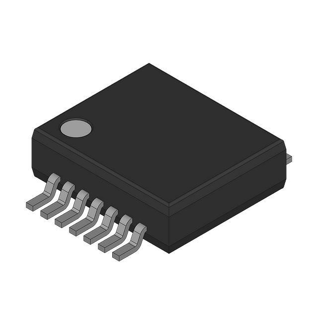
SN74HC00 . . . D, N, OR PW PACKAGE
(TOP VIEW)
Package Options Include Plastic
Small-Outline (D), Thin Shrink
Small-Outline (PW), and Ceramic Flat (W)
Packages, Ceramic Chip Carriers (FK), and
Standard Plastic (N) and Ceramic (J)
300-mil DIPs
1A
1B
1Y
2A
2B
2Y
GND
description
These devices contain four independent 2-input
NAND gates. They perform the Boolean function
Y = A • B or Y = A + B in positive logic.
The SN54HC00 is characterized for operation
over the full military temperature range of –55°C
to 125°C. The SN74HC00 is characterized for
operation from –40°C to 85°C.
B
H
H
L
L
X
H
X
L
H
2
13
3
12
4
11
5
10
6
9
7
8
VCC
4B
4A
4Y
3B
3A
3Y
1B
1A
NC
VCC
4B
1Y
NC
2A
NC
2B
4
3 2 1 20 19
18
5
17
6
16
7
15
8
14
9 10 11 12 13
4A
NC
4Y
NC
3B
2Y
GND
NC
3Y
3A
A
OUTPUT
Y
14
SN54HC00 . . . FK PACKAGE
(TOP VIEW)
FUNCTION TABLE
(each gate)
INPUTS
1
logic symbol†
NC – No internal connection
1A
1B
2A
2B
3A
3B
4A
4B
1
&
2
3
1Y
4
6
5
2Y
9
8
10
3Y
12
11
13
4Y
† This symbol is in accordance with ANSI/IEEE Std 91-1984 and IEC Publication 617-12.
Pin numbers shown are for the D, J, N, PW, and W packages.
logic diagram (positive logic)
A
Y
B
Please be aware that an important notice concerning availability, standard warranty, and use in critical applications of
Texas Instruments semiconductor products and disclaimers thereto appears at the end of this data sheet.
Copyright 1997, Texas Instruments Incorporated
PRODUCTION DATA information is current as of publication date.
Products conform to specifications per the terms of Texas Instruments
standard warranty. Production processing does not necessarily include
testing of all parameters.
POST OFFICE BOX 655303
• DALLAS, TEXAS 75265
1
�SN54HC00, SN74HC00
QUADRUPLE 2-INPUT POSITIVE-NAND GATES
SCLS181B – DECEMBER 1982 – REVISED MAY 1997
absolute maximum ratings over operating free-air temperature range†
Supply voltage range, VCC . . . . . . . . . . . . . . . . . . . . . . . . . . . . . . . . . . . . . . . . . . . . . . . . . . . . . . . . . . –0.5 V to 7 V
Input clamp current, IIK (VI < 0 or VI > VCC) (see Note 1) . . . . . . . . . . . . . . . . . . . . . . . . . . . . . . . . . . . . ±20 mA
Output clamp current, IOK (VO < 0 or VO > VCC) (see Note 1) . . . . . . . . . . . . . . . . . . . . . . . . . . . . . . . . ±20 mA
Continuous output current, IO (VO = 0 to VCC) . . . . . . . . . . . . . . . . . . . . . . . . . . . . . . . . . . . . . . . . . . . . . . ±25 mA
Continuous current through VCC or GND . . . . . . . . . . . . . . . . . . . . . . . . . . . . . . . . . . . . . . . . . . . . . . . . . . . ±50 mA
Package thermal impedance, θJA (see Note 2): D package . . . . . . . . . . . . . . . . . . . . . . . . . . . . . . . . . . 127°C/W
N package . . . . . . . . . . . . . . . . . . . . . . . . . . . . . . . . . . . 78°C/W
PW package . . . . . . . . . . . . . . . . . . . . . . . . . . . . . . . . 170°C/W
Storage temperature range, Tstg . . . . . . . . . . . . . . . . . . . . . . . . . . . . . . . . . . . . . . . . . . . . . . . . . . . –65°C to 150°C
† Stresses beyond those listed under “absolute maximum ratings” may cause permanent damage to the device. These are stress ratings only, and
functional operation of the device at these or any other conditions beyond those indicated under “recommended operating conditions” is not
implied. Exposure to absolute-maximum-rated conditions for extended periods may affect device reliability.
NOTES: 1. The input and output voltage ratings may be exceeded if the input and output current ratings are observed.
2. The package thermal impedance is calculated in accordance with JESD 51, except for through-hole packages, which use a trace
length of zero.
recommended operating conditions
SN54HC00
VCC
Supply voltage
VIH
High-level input voltage
VCC = 2 V
VCC = 4.5 V
VCC = 6 V
VCC = 2 V
VIL
Low-level input voltage
VI
VO
Input voltage
Output voltage
tt
Input transition (rise and fall) time
TA
2
SN74HC00
MIN
NOM
MAX
MIN
NOM
MAX
2
5
6
2
5
6
1.5
1.5
3.15
3.15
4.2
4.2
0.5
0
0.5
0
1.35
0
1.35
0
1.8
0
1.8
0
0
0
VCC
VCC
0
VCC
VCC
VCC = 2 V
VCC = 4.5 V
0
1000
0
1000
0
500
0
500
VCC = 6 V
0
400
0
400
–55
125
–40
85
Operating free-air temperature
POST OFFICE BOX 655303
• DALLAS, TEXAS 75265
V
V
0
VCC = 4.5 V
VCC = 6 V
UNIT
V
V
V
ns
°C
�SN54HC00, SN74HC00
QUADRUPLE 2-INPUT POSITIVE-NAND GATES
SCLS181B – DECEMBER 1982 – REVISED MAY 1997
electrical characteristics over recommended operating free-air temperature range (unless
otherwise noted)
PARAMETER
TEST CONDITIONS
VCC
IOH = –20 µA
VOH
VI = VIH or VIL
IOH = –4 mA
IOH = –5.2 mA
IOL = 20 µA
VOL
VI = VIH or VIL
IOL = 4 mA
IOL = 5.2 mA
II
ICC
VI = VCC or 0
VI = VCC or 0,
IO = 0
MIN
TA = 25°C
TYP
MAX
SN74HC00
MIN
MIN
MAX
2V
1.9
1.998
1.9
1.9
4.5 V
4.4
4.499
4.4
4.4
6V
5.9
5.999
5.9
5.9
4.5 V
3.98
4.3
3.7
3.84
6V
5.48
5.8
5.2
MAX
UNIT
V
5.34
2V
0.002
0.1
0.1
0.1
4.5 V
0.001
0.1
0.1
0.1
6V
0.001
0.1
0.1
0.1
4.5 V
0.17
0.26
0.4
0.33
6V
0.15
0.26
0.4
0.33
6V
±0.1
±100
±1000
±1000
nA
2
40
20
µA
3
10
10
10
pF
6V
Ci
SN54HC00
2 V to 6 V
V
switching characteristics over recommended operating free-air temperature range, CL = 50 pF
(unless otherwise noted) (see Figure 1)
TA = 25°C
TYP
MAX
SN54HC00
SN74HC00
MIN
MIN
PARAMETER
FROM
(INPUT)
TO
(OUTPUT)
VCC
2V
45
90
135
115
tpd
A or B
Y
4.5 V
9
18
27
23
6V
8
15
23
20
tt
Y
MIN
MAX
MAX
2V
38
75
110
95
4.5 V
8
15
22
19
6V
6
13
19
16
UNIT
ns
ns
operating characteristics, TA = 25°C
PARAMETER
Cpd
TEST CONDITIONS
Power dissipation capacitance per gate
POST OFFICE BOX 655303
No load
• DALLAS, TEXAS 75265
TYP
20
UNIT
pF
3
�SN54HC00, SN74HC00
QUADRUPLE 2-INPUT POSITIVE-NAND GATES
SCLS181B – DECEMBER 1982 – REVISED MAY 1997
PARAMETER MEASUREMENT INFORMATION
From Output
Under Test
Test
Point
Input
VCC
50%
50%
0V
CL = 50 pF
(see Note A)
tPLH
In-Phase
Output
LOAD CIRCUIT
50%
10%
tPHL
90%
90%
tr
Input
50%
10%
90%
90%
tr
tPHL
VCC
50%
10% 0 V
Out-of-Phase
Output
90%
tf
VOH
50%
10%
VOL
tf
tPLH
50%
10%
tf
50%
10%
90%
VOH
VOL
tr
VOLTAGE WAVEFORMS
PROPAGATION DELAY AND OUTPUT TRANSITION TIMES
VOLTAGE WAVEFORM
INPUT RISE AND FALL TIMES
NOTES: A. CL includes probe and test-fixture capacitance.
B. Phase relationships between waveforms were chosen arbitrarily. All input pulses are supplied by generators having the following
characteristics: PRR ≤ 1 MHz, ZO = 50 Ω, tr = 6 ns, tf = 6 ns.
C. The outputs are measured one at a time with one input transition per measurement.
D. tPLH and tPHL are the same as tpd.
Figure 1. Load Circuit and Voltage Waveforms
4
POST OFFICE BOX 655303
• DALLAS, TEXAS 75265
�IMPORTANT NOTICE
Texas Instruments and its subsidiaries (TI) reserve the right to make changes to their products or to discontinue
any product or service without notice, and advise customers to obtain the latest version of relevant information
to verify, before placing orders, that information being relied on is current and complete. All products are sold
subject to the terms and conditions of sale supplied at the time of order acknowledgement, including those
pertaining to warranty, patent infringement, and limitation of liability.
TI warrants performance of its semiconductor products to the specifications applicable at the time of sale in
accordance with TI’s standard warranty. Testing and other quality control techniques are utilized to the extent
TI deems necessary to support this warranty. Specific testing of all parameters of each device is not necessarily
performed, except those mandated by government requirements.
CERTAIN APPLICATIONS USING SEMICONDUCTOR PRODUCTS MAY INVOLVE POTENTIAL RISKS OF
DEATH, PERSONAL INJURY, OR SEVERE PROPERTY OR ENVIRONMENTAL DAMAGE (“CRITICAL
APPLICATIONS”). TI SEMICONDUCTOR PRODUCTS ARE NOT DESIGNED, AUTHORIZED, OR
WARRANTED TO BE SUITABLE FOR USE IN LIFE-SUPPORT DEVICES OR SYSTEMS OR OTHER
CRITICAL APPLICATIONS. INCLUSION OF TI PRODUCTS IN SUCH APPLICATIONS IS UNDERSTOOD TO
BE FULLY AT THE CUSTOMER’S RISK.
In order to minimize risks associated with the customer’s applications, adequate design and operating
safeguards must be provided by the customer to minimize inherent or procedural hazards.
TI assumes no liability for applications assistance or customer product design. TI does not warrant or represent
that any license, either express or implied, is granted under any patent right, copyright, mask work right, or other
intellectual property right of TI covering or relating to any combination, machine, or process in which such
semiconductor products or services might be or are used. TI’s publication of information regarding any third
party’s products or services does not constitute TI’s approval, warranty or endorsement thereof.
Copyright 1998, Texas Instruments Incorporated
�1 of 3
Products
Development Tools
Applications
Search
PRODUCT FOLDER | PRODUCT INFO: FEATURES | DESCRIPTION | DATASHEETS |
PRICING/AVAILABILITY | APPLICATION NOTES |
RELATED DOCUMENTS
PRODUCT SUPPORT: TRAINING
SN54HC00, Quadruple 2-Input Positive-NAND Gates
DEVICE STATUS: ACTIVE
PARAMETER NAME SN54HC00
Voltage Nodes (V) 6, 5, 2
Vcc range (V)
2.0 to 6.0
Input Level
CMOS
Output Level
CMOS
No. of Gates
4
FEATURES
l
Back to Top
Package Options Include Plastic Small-Outline (D), Thin Shrink Small-Outline (PW), and
Ceramic Flat (W) Packages, Ceramic Chip Carriers (FK), and Standard Plastic (N) and
Ceramic (J) 300-mil DIPs
DESCRIPTION
Back to Top
These devices contain four independent 2-input NAND gates. They perform the Boolean
function Y = A \•\ B\ or Y = A\ + B\ in positive logic.
The SN54HC00 is characterized for operation over the full military temperature range of -55°C
to 125°C. The SN74HC00 is characterized for operation from -40°C to 85°C.
TECHNICAL DOCUMENTS
Back to Top
To view the following documents, Acrobat Reader 3.x is required.
To download a document to your hard drive, right-click on the link and choose 'Save'.
DATASHEET
Back to Top
Full datasheet in Acrobat PDF: scls181b.pdf (76 KB) ( Updated: 05/01/1997)
Full datasheet in Zipped PostScript: scls181b.psz (76 KB)
APPLICATION NOTES
View Application Reports for Digital Logic
Back to Top
�2 of 3
l
l
l
l
l
l
l
l
CMOS Power Consumption And CPD Calculation (SCAA035B - Updated: 06/01/1997)
Designing With Logic (SDYA009C - Updated: 06/01/1997)
HCMOS Design Considerations (SCLA007 - Updated: 04/01/1996)
Implications of Slow or Floating CMOS Inputs (SCBA004C - Updated: 02/01/1998)
Input and Output Characteristics of Digital Integrated Circuits (SDYA010 - Updated:
10/01/1996)
Live Insertion (SDYA012 - Updated: 10/01/1996)
SN54/74HCT CMOS Logic Family Applications And Restrictions (SCLA011 - Updated:
05/01/1996)
Using High Speed CMOS And Advanced CMOS In Systems With Multiple Vcc (SCLA008 Updated: 04/01/1996)
Back to Top
RELATED DOCUMENTS
l
l
l
l
Documentation Rules (SAP) And Ordering Information (SZZU001B, 4 KB - Updated:
05/06/1999)
Logic Selection Guide Second Half 2000 (SDYU001N, 5035 KB - Updated: 04/17/2000)
MicroStar Junior BGA Design Summary (SCET004, 167 KB - Updated: 07/28/2000)
More Power In Less Space - Technical Article (SCAU001A, 850 KB - Updated: 03/01/1996)
Back to Top
PRICING/AVAILABILITY
ORDERABLE
DEVICE
TEMP
PACKAGE PINS
STATUS
(ºC)
BUDGETARY
PRICE
US$/UNIT
QTY=1000+
PACK
QTY
DSCC
NUMBER
PRICING/AVAILABILITY
84037012A
FK
20
-55
TO
125
ACTIVE
6.71
1
Check stock or order
8403701DA
W
14
-55
TO
125
ACTIVE
8.29
1
Check stock or order
JM38510/65001B2A
FK
20
-55
TO
125
ACTIVE
7.65
1
Check stock or order
JM38510/65001BCA
J
14
-55
TO
125
ACTIVE
3.93
1
Check stock or order
JM38510/65001BDA
W
14
-55
TO
125
ACTIVE
9.30
1
Check stock or order
SN54HC00J
J
14
-55
TO
125
ACTIVE
0.87
1
Check stock or order
SNJ54HC00FK
FK
20
-55
TO
125
ACTIVE
6.71
1
SNJ54HC00J
J
14
-55
TO
125
ACTIVE
1.03
1
-55
84037012A
Check stock or order
Check stock or order
�3 of 3
SNJ54HC00W
W
14
TO
125
ACTIVE
8.29
1
8403701DA
Table Data Updated on: 11/10/2000
© Copyright 2000 Texas Instruments Incorporated. All rights reserved. Trademarks | Privacy Policy
| Important Notice
Check stock or order
�1 of 3
Products
Development Tools
Applications
Search
PRODUCT FOLDER | PRODUCT INFO: FEATURES | DESCRIPTION | DATASHEETS |
PRICING/AVAILABILITY | APPLICATION NOTES |
RELATED DOCUMENTS
PRODUCT SUPPORT: TRAINING
SN74HC00, Quadruple 2-Input Positive-NAND Gates
DEVICE STATUS: ACTIVE
PARAMETER NAME SN74HC00
Voltage Nodes (V) 6, 5, 2
Vcc range (V)
2.0 to 6.0
Input Level
CMOS
Output Level
CMOS
Output Drive (mA) -4/4
No. of Gates
4
Static Current
0.02
tpd(max) (ns)
20
FEATURES
l
Back to Top
Package Options Include Plastic Small-Outline (D), Thin Shrink Small-Outline (PW), and
Ceramic Flat (W) Packages, Ceramic Chip Carriers (FK), and Standard Plastic (N) and
Ceramic (J) 300-mil DIPs
DESCRIPTION
Back to Top
These devices contain four independent 2-input NAND gates. They perform the Boolean
function Y = A \•\ B\ or Y = A\ + B\ in positive logic.
The SN54HC00 is characterized for operation over the full military temperature range of -55°C
to 125°C. The SN74HC00 is characterized for operation from -40°C to 85°C.
TECHNICAL DOCUMENTS
Back to Top
To view the following documents, Acrobat Reader 3.x is required.
To download a document to your hard drive, right-click on the link and choose 'Save'.
DATASHEET
Back to Top
Full datasheet in Acrobat PDF: scls181b.pdf (76 KB) ( Updated: 05/01/1997)
�2 of 3
Full datasheet in Zipped PostScript: scls181b.psz (76 KB)
Back to Top
APPLICATION NOTES
View Application Reports for Digital Logic
l
l
l
l
l
l
l
l
CMOS Power Consumption and CPD Calculation (SCAA035B - Updated: 06/01/1997)
Designing With Logic (SDYA009C - Updated: 06/01/1997)
HCMOS Design Considerations (SCLA007 - Updated: 04/01/1996)
Implications of Slow or Floating CMOS Inputs (SCBA004C - Updated: 02/01/1998)
Input and Output Characteristics of Digital Integrated Circuits (SDYA010 - Updated:
10/01/1996)
Live Insertion (SDYA012 - Updated: 10/01/1996)
SN54/74HCT CMOS Logic Family Applications And Restrictions (SCLA011 - Updated:
05/01/1996)
Using High Speed CMOS and Advanced CMOS In Systems With Multiple Vcc (SCLA008 Updated: 04/01/1996)
Back to Top
RELATED DOCUMENTS
l
l
l
l
Documentation Rules (SAP) And Ordering Information (SZZU001B, 4 KB - Updated:
05/06/1999)
Logic Selection Guide Second Half 2000 (SDYU001N, 5035 KB - Updated: 04/17/2000)
MicroStar Junior BGA Design Summary (SCET004, 167 KB - Updated: 07/28/2000)
More Power In Less Space - Technical Article (SCAU001A, 850 KB - Updated: 03/01/1996)
Back to Top
PRICING/AVAILABILITY
ORDERABLE
DEVICE
PACKAGE PINS
TEMP
(ºC)
STATUS
BUDGETARY
PRICE
US$/UNIT
QTY=1000+
PACK
QTY
PRICING/AVAILABILITY
SN74HC00ADBLE
DB
14
-40 TO
85
OBSOLETE
SN74HC00ADBR
DB
14
-40 TO
85
NRND
0.33
2000
Check stock or order
SN74HC00D
D
14
-40 TO
85
ACTIVE
0.25
50
Check stock or order
SN74HC00DR
D
14
-40 TO
85
ACTIVE
0.28
2500
Check stock or order
SN74HC00N
N
14
-40 TO
85
ACTIVE
0.23
25
Check stock or order
SN74HC00N3
N
14
-40 TO
85
OBSOLETE
SN74HC00NSR
NS
14
-40 TO
85
ACTIVE
0.33
2000
Check stock or order
SN74HC00PWLE
PW
14
-40 TO
85
OBSOLETE
SN74HC00PWR
PW
14
-40 TO
85
ACTIVE
0.25
2000
Check stock or order
�3 of 3
Table Data Updated on: 11/15/2000
© Copyright 2000 Texas Instruments Incorporated. All rights reserved. Trademarks | Privacy Policy
| Important Notice
�


 工商网监
湘ICP备2023018690号
工商网监
湘ICP备2023018690号
