��������
��
�
�
� ����������� ������� �������
����� ����� �
�� ������
SCLS594A − NOVEMBER 2004 − REVISED APRIL 2008
D
D
D
D
D
D
D
D
D Fully Synchronous in Count Modes
D Parallel Asynchronous Load for Modulo-N
Qualified for Automotive Applications
Wide Operating Voltage Range of 2 V to 6 V
Outputs Can Drive Up To 10 LSTTL Loads
Low Power Consumption, 80-µA Max ICC
Typical tpd = 20 ns
±4-mA Output Drive at 5 V
Low Input Current of 1 µA Max
Look-Ahead Circuitry Enhances Cascaded
Counters
Count Lengths
D Asynchronous Clear
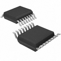
PW PACKAGE
(TOP VIEW)
B
QB
QA
DOWN
UP
QC
QD
GND
description/ordering information
The SN74HC193 device is a 4-bit synchronous,
reversible, up/down binary counter. Synchronous
operation is provided by having all flip-flops clocked
simultaneously so that the outputs change
simultaneously with each other when dictated by the
steering logic. This mode of operation eliminates the
output counting spikes normally associated with
asynchronous (ripple-clock) counters.
1
16
2
15
3
14
4
13
5
12
6
11
7
10
8
9
VCC
A
CLR
BO
CO
LOAD
C
D
The outputs of the four flip-flops are triggered on a low-to-high-level transition of either count (clock) input (UP
or DOWN). The direction of counting is determined by which count input is pulsed while the other count input
is high.
All four counters are fully programmable; that is, each output may be preset to either level by placing a low on
the load (LOAD) input and entering the desired data at the data inputs. The output changes to agree with the
data inputs independently of the count pulses. This feature allows the counters to be used as modulo-N dividers
simply by modifying the count length with the preset inputs.
A clear (CLR) input has been provided that forces all outputs to the low level when a high level is applied. The
clear function is independent of the count and LOAD inputs.
This counter was designed to be cascaded without the need for external circuitry. The borrow (BO) output
produces a low-level pulse while the count is zero (all outputs low) and DOWN is low. Similarly, the carry (CO)
output produces a low-level pulse while the count is maximum (9 or 15), and UP is low. The counter then can
be cascaded easily by feeding BO and CO to DOWN and UP, respectively, of the succeeding counter.
ORDERING INFORMATION{
−40°C to 125°C
ORDERABLE
PART NUMBER
PACKAGE‡
TA
TSSOP − PW
Reel of 2000
TOP-SIDE
MARKING
SN74HC193QPWRQ1
HC193Q
−40°C to 85°C
TSSOP − PW
Reel of 2000
SN74HC193IPWRQ1
HC193I
† For the most current package and ordering information, see the Package Option Addendum at the end of
this document, or see the TI web site at http://www.ti.com.
‡ Package drawings, thermal data, and symbolization are available at http://www.ti.com/packaging.
Please be aware that an important notice concerning availability, standard warranty, and use in critical applications of
Texas Instruments semiconductor products and disclaimers thereto appears at the end of this data sheet.
Copyright 2008, Texas Instruments Incorporated
�������
�� ���� ���!"#$%�!� �& '("")�% $& !� *(+,�'$%�!� -$%).
�"!-('%& '!��!"# %! &*)'���'$%�!�& *)" %/) %)"#& !� �)0$&
�&%"(#)�%&
&%$�-$"- 1$""$�%2. �"!-('%�!� *"!')&&��3 -!)& �!% �)')&&$"�,2 ��',(-)
%)&%��3 !� $,, *$"$#)%)"&.
POST OFFICE BOX 655303
• DALLAS, TEXAS 75265
1
���������
��
�
�
� ����������� ������� �������
����� ����� �
�� ������
SCLS594A − NOVEMBER 2004 − REVISED APRIL 2008
logic diagram (positive logic)
12
13
CLR
UP
DOWN
LOAD
A
5
4
S
11
R
15
S
3
2
C1
1D
R
6
C1
1D
R
QC
9
S
C1
1D
R
2
QB
10
S
D
QA
1
S
C
BO
14
C1
1D
R
B
CO
POST OFFICE BOX 655303
• DALLAS, TEXAS 75265
7
QD
���������
��
�
�
� ����������� ������� �������
����� ����� �
�� ������
SCLS594A − NOVEMBER 2004 − REVISED APRIL 2008
typical clear, load, and count sequence
The following sequence is illustrated below:
1. Clear outputs to 0
2. Load (preset) to binary 13
3. Count up to 14, 15, carry, 0, 1, and 2
4. Count down to 1, 0, borrow, 15, 14, and 13
CLR
LOAD
A
Data
Inputs
B
C
D
UP
DOWN
QA
Data
Outputs
QB
QC
QD
CO
BO
0
13
Clear
Preset
14
15
0
Count Up
1
2
1
0
15
14
Count Down
13
NOTES: A. CLR overrides LOAD, data, and count inputs.
B. When counting up, count-down input must be high; when counting down, count-up input must be high.
POST OFFICE BOX 655303
• DALLAS, TEXAS 75265
3
���������
��
�
�
� ����������� ������� �������
����� ����� �
�� ������
SCLS594A − NOVEMBER 2004 − REVISED APRIL 2008
absolute maximum ratings over operating free-air temperature range (unless otherwise noted)†
Supply voltage range, VCC . . . . . . . . . . . . . . . . . . . . . . . . . . . . . . . . . . . . . . . . . . . . . . . . . . . . . . . . . . −0.5 V to 7 V
Input clamp current, IIK (VI < 0 or VI > VCC) (see Note 1) . . . . . . . . . . . . . . . . . . . . . . . . . . . . . . . . . . . . ±20 mA
Output clamp current, IOK (VO < 0 or VO > VCC) (see Note 1) . . . . . . . . . . . . . . . . . . . . . . . . . . . . . . . . ±20 mA
Continuous output current, IO (VO = 0 to VCC) . . . . . . . . . . . . . . . . . . . . . . . . . . . . . . . . . . . . . . . . . . . . . . ±25 mA
Continuous current through VCC or GND . . . . . . . . . . . . . . . . . . . . . . . . . . . . . . . . . . . . . . . . . . . . . . . . . . . ±50 mA
Package thermal impedance, θJA (see Note 2) . . . . . . . . . . . . . . . . . . . . . . . . . . . . . . . . . . . . . . . . . . . . 108°C/W
Storage temperature range, Tstg . . . . . . . . . . . . . . . . . . . . . . . . . . . . . . . . . . . . . . . . . . . . . . . . . . . −65°C to 150°C
† Stresses beyond those listed under “absolute maximum ratings” may cause permanent damage to the device. These are stress ratings only, and
functional operation of the device at these or any other conditions beyond those indicated under “recommended operating conditions” is not
implied. Exposure to absolute-maximum-rated conditions for extended periods may affect device reliability.
NOTES: 1. The input and output voltage ratings may be exceeded if the input and output current ratings are observed.
2. The package thermal impedance is calculated in accordance with JESD 51-7.
recommended operating conditions (see Note 3)
VCC
VIH
Supply voltage
VCC = 2 V
VCC = 4.5 V
High-level input voltage
VCC = 6 V
VCC = 2 V
VIL
VI
VO
∆t/∆v‡
TA
MIN
NOM
MAX
2
5
6
Input voltage
3.15
0.5
1.35
0
Operating free-air temperature
V
1.8
VCC = 2 V
VCC = 4.5 V
Input transition rise/fall time
V
4.2
0
Output voltage
V
1.5
VCC = 4.5 V
VCC = 6 V
Low-level input voltage
UNIT
VCC
VCC
V
V
1000
500
VCC = 6 V
Q-suffix devices
−40
125
I-suffix devices
−40
85
ns
400
°C
NOTE 3: All unused inputs of the device must be held at VCC or GND to ensure proper device operation. Refer to the TI application report,
Implications of Slow or Floating CMOS Inputs, literature number SCBA004.
‡ If this device is used in the threshold region (from VILmax = 0.5 V to VIHmin = 1.5 V), there is a potential to go into the wrong state from induced
grounding, causing double clocking. Operating with the inputs at tt = 1000 ns and VCC = 2 V does not damage the device; however, functionally,
the CLK inputs are not ensured while in the shift, count, or toggle operating modes.
4
POST OFFICE BOX 655303
• DALLAS, TEXAS 75265
���������
��
�
�
� ����������� ������� �������
����� ����� �
�� ������
SCLS594A − NOVEMBER 2004 − REVISED APRIL 2008
electrical characteristics over recommended operating free-air temperature range (unless
otherwise noted)
PARAMETER
TEST CONDITIONS
IOH = −20 µA
VOH
VI = VIH or VIL
IOH = −4 mA
IOH = −5.2 mA
VOL
II
ICC
Ci
MAX
TA = −40°C
TO 125°C
TA = −40°C
TO 85°C
MIN
MIN
MIN
TYP
2V
1.9
1.998
1.9
1.9
4.5 V
4.4
4.499
4.4
4.4
6V
5.9
5.999
5.9
5.9
4.5 V
3.98
4.3
3.7
3.84
6V
5.48
5.8
MAX
5.2
UNIT
MAX
V
5.34
2V
0.002
0.1
0.1
0.1
IOL = 20 µA
4.5 V
0.001
0.1
0.1
0.1
6V
0.001
0.1
0.1
0.1
IOL = 4 mA
IOL = 5.2 mA
4.5 V
0.17
0.26
0.4
0.33
6V
0.15
0.26
0.4
0.33
6V
±0.1
±100
±1000
±1000
nA
8
160
80
µA
10
10
10
pF
VI = VIH or VIL
VI = VCC or 0
VI = VCC or 0,
TA = 25°C
VCC
IO = 0
6V
2 V to 6 V
POST OFFICE BOX 655303
3
• DALLAS, TEXAS 75265
V
5
���������
��
�
�
� ����������� ������� �������
����� ����� �
�� ������
SCLS594A − NOVEMBER 2004 − REVISED APRIL 2008
timing requirements over recommended operating free-air temperature range (unless otherwise
noted)
VCC
fclock
Clock frequency
CLR high
tw
Pulse duration
LOAD low
UP or DOWN, high or low
Data before LOAD inactive
tsu
Setup time
CLR inactive before UP↑ or DOWN↓
LOAD inactive before UP↑ or DOWN↓
th
6
Hold time
Data after LOAD inactive
POST OFFICE BOX 655303
TA = 25°C
TA = −40°C
TO 125°C
TA = −40°C
TO 85°C
MIN
MIN
MIN
MAX
MAX
2V
4.2
2.8
3.3
4.5 V
21
14
17
6V
24
16
19
2V
120
180
150
4.5 V
24
36
30
6V
21
31
26
2V
120
180
150
4.5 V
24
36
30
6V
21
31
26
2V
120
180
150
4.5 V
24
36
30
6V
21
31
26
2V
110
165
140
4.5 V
22
33
28
6V
19
28
24
2V
110
165
140
4.5 V
22
33
28
6V
19
28
24
2V
110
165
140
4.5 V
22
33
28
6V
19
28
24
2V
5
5
5
4.5 V
5
5
5
6V
5
5
5
• DALLAS, TEXAS 75265
UNIT
MAX
MHz
ns
ns
ns
���������
��
�
�
� ����������� ������� �������
����� ����� �
�� ������
SCLS594A − NOVEMBER 2004 − REVISED APRIL 2008
switching characteristics over recommended operating free-air temperature range, CL = 50 pF
(unless otherwise noted) (see Figure 1)
PARAMETER
FROM
(INPUT)
TO
(OUTPUT)
fmax
UP
DOWN
CO
BO
tpd
UP or DOWN
LOAD
tPHL
CLR
tt
Any Q
Any Q
Any Q
Any
TA = 25°C
VCC
MAX
TA = −40°C
TO 125°C
TA = −40°C
TO 85°C
MIN
MIN
MIN
TYP
MAX
2V
4.2
8
2.8
3.3
4.5 V
21
55
14
17
6V
24
60
16
19
UNIT
MAX
MHz
2V
75
165
250
205
4.5 V
24
33
50
41
6V
20
28
43
35
2V
75
165
250
205
4.5 V
24
33
50
41
6V
20
28
43
35
2V
190
250
375
315
4.5 V
40
50
75
63
6V
35
43
64
54
2V
190
260
390
325
4.5 V
40
52
78
65
6V
35
44
66
55
2V
170
240
360
300
4.5 V
36
48
72
60
6V
31
41
61
51
2V
38
75
110
95
4.5 V
8
15
22
19
6V
6
14
19
17
ns
ns
ns
operating characteristics, TA = 25°C
PARAMETER
Cpd
TEST CONDITIONS
Power dissipation capacitance
No load
POST OFFICE BOX 655303
• DALLAS, TEXAS 75265
TYP
50
UNIT
pF
7
���������
��
�
�
� ����������� ������� �������
����� ����� �
�� ������
SCLS594A − NOVEMBER 2004 − REVISED APRIL 2008
PARAMETER MEASUREMENT INFORMATION
From Output
Under Test
VCC
High-Level
Pulse
Test
Point
50%
50%
0V
tw
CL = 50 pF
(see Note A)
VCC
Low-Level
Pulse
50%
50%
0V
LOAD CIRCUIT
VOLTAGE WAVEFORMS
PULSE DURATIONS
Input
VCC
50%
50%
0V
tPLH
Reference
Input
VCC
50%
In-Phase
Output
0V
tsu
Data
Input 50%
10%
90%
tr
tPHL
VCC
50%
10% 0 V
90%
90%
tr
th
90%
50%
10%
tPHL
Out-of-Phase
Output
90%
VOLTAGE WAVEFORMS
SETUP AND HOLD AND INPUT RISE AND FALL TIMES
tPLH
50%
10%
tf
tf
VOH
50%
10%
VOL
tf
50%
10%
90%
VOH
VOL
tr
VOLTAGE WAVEFORMS
PROPAGATION DELAY AND OUTPUT TRANSITION TIMES
NOTES: A. CL includes probe and test-fixture capacitance.
B. Phase relationships between waveforms were chosen arbitrarily. All input pulses are supplied by generators having the following
characteristics: PRR ≤ 1 MHz, ZO = 50 Ω, tr = 6 ns, tf = 6 ns.
C. For clock inputs, fmax is measured when the input duty cycle is 50%.
D. The outputs are measured one at a time, with one input transition per measurement.
E. tPLH and tPHL are the same as tpd.
Figure 1. Load Circuit and Voltage Waveforms
8
POST OFFICE BOX 655303
• DALLAS, TEXAS 75265
�PACKAGE OPTION ADDENDUM
www.ti.com
10-Dec-2020
PACKAGING INFORMATION
Orderable Device
Status
(1)
Package Type Package Pins Package
Drawing
Qty
Eco Plan
(2)
Lead finish/
Ball material
MSL Peak Temp
Op Temp (°C)
Device Marking
(3)
(4/5)
(6)
SN74HC193QPWRG4Q1
ACTIVE
TSSOP
PW
16
2000
RoHS & Green
NIPDAU
Level-1-260C-UNLIM
-40 to 125
HC193Q
(1)
The marketing status values are defined as follows:
ACTIVE: Product device recommended for new designs.
LIFEBUY: TI has announced that the device will be discontinued, and a lifetime-buy period is in effect.
NRND: Not recommended for new designs. Device is in production to support existing customers, but TI does not recommend using this part in a new design.
PREVIEW: Device has been announced but is not in production. Samples may or may not be available.
OBSOLETE: TI has discontinued the production of the device.
(2)
RoHS: TI defines "RoHS" to mean semiconductor products that are compliant with the current EU RoHS requirements for all 10 RoHS substances, including the requirement that RoHS substance
do not exceed 0.1% by weight in homogeneous materials. Where designed to be soldered at high temperatures, "RoHS" products are suitable for use in specified lead-free processes. TI may
reference these types of products as "Pb-Free".
RoHS Exempt: TI defines "RoHS Exempt" to mean products that contain lead but are compliant with EU RoHS pursuant to a specific EU RoHS exemption.
Green: TI defines "Green" to mean the content of Chlorine (Cl) and Bromine (Br) based flame retardants meet JS709B low halogen requirements of


 工商网监
湘ICP备2023018690号
工商网监
湘ICP备2023018690号
