SN54HC534, SN74HC534
OCTAL EDGE-TRIGGERED D-TYPE FLIP-FLOPS
WITH 3-STATE OUTPUTS
SCLS311A – JANUARY 1996 – REVISED MAY 1997
D
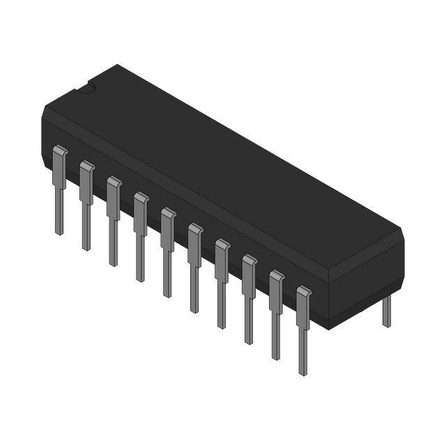
SN54HC534 . . . J OR W PACKAGE
SN74HC534 . . . DW OR N PACKAGE
(TOP VIEW)
High-Current 3-State Inverting Outputs Can
Drive up to 15 LSTTL Loads
Package Options Include Plastic
Small-Outline (DW) and Ceramic Flat (W)
Packages, Ceramic Chip Carriers (FK), and
Standard Plastic (N) and Ceramic (J)
300-mil DIPs
OE
1Q
1D
2D
2Q
3Q
3D
4D
4Q
GND
description
These 8-bit flip-flops feature 3-state outputs
designed specifically for driving highly capacitive
or relatively low-impedance loads. They are
particularly suitable for implementing buffer
registers, I/O ports, bidirectional bus drivers, and
working registers.
1
20
2
19
3
18
4
17
5
16
6
15
7
14
8
13
9
12
10
11
VCC
8Q
8D
7D
7Q
6Q
6D
5D
5Q
CLK
SN54HC534 . . . FK PACKAGE
(TOP VIEW)
1D
1Q
OE
VCC
The eight flip-flops of the ’HC534 are
edge-triggered D-type flip-flops. On the positive
transition of the clock (CLK) input, the Q outputs
are set to the complement of the logic states that
were set up at the data (D) inputs. The ’HC534 are
functionally equivalent to the ’HC374, but the
’HC534 have inverted outputs.
2D
2Q
3Q
3D
4D
4
3 2 1 20 19
18
5
17
6
16
7
15
8
14
9 10 11 12 13
8D
7D
7Q
6Q
6D
4Q
GND
CLK
5Q
5D
An output-enable (OE) input places the eight
outputs in either a normal logic state (high or low
logic levels) or the high-impedance state. In the
high-impedance state, the outputs neither load
nor drive the bus lines significantly. The
high-impedance state and increased drive
provide the capability to drive bus lines without
interface or pullup components.
8Q
D
OE does not affect the internal operations of the flip-flops. Old data can be retained or new data can be entered
while the outputs are off.
The SN54HC534 is characterized for operation over the full military temperature range of –55°C to 125°C. The
SN74HC534 is characterized for operation from –40°C to 85°C.
FUNCTION TABLE
(each flip-flop)
INPUTS
OE
CLK
D
OUTPUT
Q
L
↑
H
L
L
↑
L
H
L
H or L
X
Q0
H
X
X
Z
Please be aware that an important notice concerning availability, standard warranty, and use in critical applications of
Texas Instruments semiconductor products and disclaimers thereto appears at the end of this data sheet.
Copyright 1997, Texas Instruments Incorporated
PRODUCTION DATA information is current as of publication date.
Products conform to specifications per the terms of Texas Instruments
standard warranty. Production processing does not necessarily include
testing of all parameters.
POST OFFICE BOX 655303
• DALLAS, TEXAS 75265
1
�SN54HC534, SN74HC534
OCTAL EDGE-TRIGGERED D-TYPE FLIP-FLOPS
WITH 3-STATE OUTPUTS
SCLS311A – JANUARY 1996 – REVISED MAY 1997
logic symbol†
1
OE
CLK
1D
2D
3D
4D
5D
6D
7D
8D
11
3
EN
C1
2
1D
4
5
7
6
8
9
13
12
14
15
17
16
18
19
1Q
2Q
3Q
4Q
5Q
6Q
7Q
8Q
† This symbol is in accordance with ANSI/IEEE Std 91-1984 and IEC Publication 617-12.
logic diagram (positive logic)
OE
CLK
1
11
C1
1D
3
2
1D
1Q
To Seven Other Channels
absolute maximum ratings over operating free-air temperature range‡
Supply voltage range, VCC . . . . . . . . . . . . . . . . . . . . . . . . . . . . . . . . . . . . . . . . . . . . . . . . . . . . . . . . . . –0.5 V to 7 V
Input clamp current, IIK (VI < 0 or VI > VCC) (see Note 1) . . . . . . . . . . . . . . . . . . . . . . . . . . . . . . . . . . . . ±20 mA
Output clamp current, IOK (VO < 0 or VO > VCC) (see Note 1) . . . . . . . . . . . . . . . . . . . . . . . . . . . . . . . . ±20 mA
Continuous output current, IO (VO = 0 to VCC) . . . . . . . . . . . . . . . . . . . . . . . . . . . . . . . . . . . . . . . . . . . . . . ±35 mA
Continuous current through VCC or GND . . . . . . . . . . . . . . . . . . . . . . . . . . . . . . . . . . . . . . . . . . . . . . . . . . . ±70 mA
Package thermal impedance, θJA (see Note 2): DW package . . . . . . . . . . . . . . . . . . . . . . . . . . . . . . . . . 97°C/W
N package . . . . . . . . . . . . . . . . . . . . . . . . . . . . . . . . . . . 67°C/W
Storage temperature range, Tstg . . . . . . . . . . . . . . . . . . . . . . . . . . . . . . . . . . . . . . . . . . . . . . . . . . . –65°C to 150°C
‡ Stresses beyond those listed under “absolute maximum ratings” may cause permanent damage to the device. These are stress ratings only, and
functional operation of the device at these or any other conditions beyond those indicated under “recommended operating conditions” is not
implied. Exposure to absolute-maximum-rated conditions for extended periods may affect device reliability.
NOTES: 1. The input and output voltage ratings may be exceeded if the input and output current ratings are observed.
2. The package thermal impedance is calculated in accordance with JESD 51, except for through-hole packages, which use a trace
length of zero.
2
POST OFFICE BOX 655303
• DALLAS, TEXAS 75265
�SN54HC534, SN74HC534
OCTAL EDGE-TRIGGERED D-TYPE FLIP-FLOPS
WITH 3-STATE OUTPUTS
SCLS311A – JANUARY 1996 – REVISED MAY 1997
recommended operating conditions
SN54HC534
VCC
VIH
Supply voltage
VCC = 2 V
VCC = 4.5 V
High-level input voltage
VCC = 6 V
VCC = 2 V
VIL
VI
VO
Low-level input voltage
Input voltage
Output voltage
Input transition (rise and fall) time
TA
Operating free-air temperature
NOM
MAX
2
5
6
VCC = 2 V
VCC = 4.5 V
VCC = 6 V
MIN
NOM
MAX
2
5
6
1.5
1.5
3.15
3.15
4.2
VCC = 4.5 V
VCC = 6 V
tt
SN74HC534
MIN
UNIT
V
V
4.2
0
0.5
0
0.5
0
1.35
0
1.35
0
1.8
0
1.8
0
0
0
VCC
VCC
0
VCC
VCC
0
1000
0
1000
0
500
0
500
0
400
0
400
–55
125
–40
85
V
V
V
ns
°C
electrical characteristics over recommended operating free-air temperature range (unless
otherwise noted)
PARAMETER
VOH
VOL
TEST CONDITIONS
VI = VCC or 0,
SN54HC534
MIN
MAX
SN74HC534
MIN
MAX
UNIT
2V
1.9
1.998
1.9
1.9
4.4
4.499
4.4
4.4
6V
5.9
5.999
5.9
5.9
IOH = –6 mA
IOH = –7.8 mA
4.5 V
3.98
4.3
3.7
3.84
6V
5.48
5.8
5.2
5.34
2V
0.002
0.1
0.1
0.1
IOL = 20 µA
4.5 V
0.001
0.1
0.1
0.1
6V
0.001
0.1
0.1
0.1
4.5 V
0.17
0.26
0.4
0.33
6V
0.15
0.26
0.4
0.33
6V
±0.1
±100
±1000
±1000
nA
6V
±0.01
±0.5
±10
±5
µA
8
160
80
µA
10
10
10
pF
IOL = 6 mA
IOL = 7.8 mA
ICC
Ci
TA = 25°C
TYP
MAX
4.5 V
VI = VIH or VIL
VI = VCC or 0
VO = VCC or 0,
MIN
IOH = –20 µA
VI = VIH or VIL
II
IOZ
VCC
VI = VIH or VIL
IO = 0
6V
2 V to 6 V
POST OFFICE BOX 655303
3
• DALLAS, TEXAS 75265
V
V
3
�SN54HC534, SN74HC534
OCTAL EDGE-TRIGGERED D-TYPE FLIP-FLOPS
WITH 3-STATE OUTPUTS
SCLS311A – JANUARY 1996 – REVISED MAY 1997
timing requirements over recommended operating free-air temperature range (unless otherwise
noted)
VCC
fclock
Clock frequency
tw
Pulse duration, CLK high or low
Setup time, data before CLK↑
↑
tsu
Hold time, data after CLK↑
↑
th
TA = 25°C
MIN
MAX
SN54HC534
SN74HC534
MIN
MAX
MIN
MAX
2V
0
6
0
4.2
0
5
4.5 V
0
31
0
21
0
25
6V
0
36
0
25
0
29
2V
80
120
100
4.5 V
16
24
20
6V
14
20
17
2V
100
150
125
4.5 V
20
30
25
6V
17
26
21
2V
5
5
5
4.5 V
5
5
5
6V
5
5
5
UNIT
MHz
ns
ns
ns
switching characteristics over recommended operating free-air temperature range, CL = 50 pF
(unless otherwise noted) (see Figure 1)
PARAMETER
FROM
(INPUT)
TO
(OUTPUT)
fmax
tpd
ten
tdis
tt
4
CLK
OE
OE
Any Q
Any Q
Any Q
Any Q
VCC
TA = 25°C
MIN
TYP
MAX
SN54HC534
MIN
MAX
SN74HC534
MIN
2V
6
11
4.2
5
4.5 V
31
36
21
25
6V
36
40
25
MAX
MHz
29
2V
88
180
270
225
4.5 V
28
36
54
45
6V
24
31
46
38
2V
77
150
225
190
4.5 V
26
30
45
38
6V
23
26
38
32
2V
51
150
225
190
4.5 V
25
30
45
38
6V
23
26
38
32
2V
28
60
90
75
4.5 V
8
12
18
15
6V
6
10
15
13
POST OFFICE BOX 655303
• DALLAS, TEXAS 75265
UNIT
ns
ns
ns
ns
�SN54HC534, SN74HC534
OCTAL EDGE-TRIGGERED D-TYPE FLIP-FLOPS
WITH 3-STATE OUTPUTS
SCLS311A – JANUARY 1996 – REVISED MAY 1997
switching characteristics over recommended operating free-air temperature range, CL = 150 pF
(unless otherwise noted) (see Figure 1)
PARAMETER
tpd
ten
tt
FROM
(INPUT)
CLK
OE
TO
(OUTPUT)
Any Q
Any Q
Any Q
VCC
MIN
TA = 25°C
TYP
MAX
SN54HC534
MIN
MAX
SN74HC534
MIN
MAX
2V
105
230
345
290
4.5 V
35
46
69
58
6V
31
39
58
49
2V
95
200
300
250
4.5 V
32
40
60
50
6V
29
34
51
43
2V
60
210
315
265
4.5 V
17
42
63
53
6V
14
36
53
45
UNIT
ns
ns
ns
operating characteristics, TA = 25°C
PARAMETER
Cpd
Power dissipation capacitance per flip-flop
POST OFFICE BOX 655303
• DALLAS, TEXAS 75265
TEST CONDITIONS
TYP
UNIT
No load
100
pF
5
�SN54HC534, SN74HC534
OCTAL EDGE-TRIGGERED D-TYPE FLIP-FLOPS
WITH 3-STATE OUTPUTS
SCLS311A – JANUARY 1996 – REVISED MAY 1997
PARAMETER MEASUREMENT INFORMATION
VCC
From Output
Under Test
CL
(see Note A)
PARAMETER
S1
Test
Point
tPZH
ten
RL
1 kΩ
tPZL
tPHZ
tdis
S2
RL
1 kΩ
Data
Input
VCC
50%
10%
50%
50%
0V
In-Phase
Output
50%
10%
tPHL
90%
90%
tr
tPHL
Out-ofPhase
Output
90%
tf
Closed
Closed
Open
Open
Open
VCC
th
90%
90%
VCC
50%
10% 0 V
tf
50%
10%
Output
Control
(Low-Level
Enabling)
VCC
50%
50%
0V
tPZL
VOH
50%
10% V
OL
tf
Output
Waveform 1
(See Note B)
tPLZ
≈ VCC
≈ VCC
50%
10%
VOL
tPZH
tPLH
50%
10%
Open
VOLTAGE WAVEFORMS
SETUP AND HOLD AND INPUT RISE AND FALL TIMES
VCC
tPLH
Open
tr
VOLTAGE WAVEFORMS
PULSE DURATIONS
50%
Closed
0V
0V
Input
Closed
tsu
0V
50%
Open
50%
50%
tw
Low-Level
Pulse
50 pF
or
150 pF
50 pF
or
150 pF
––
Reference
Input
VCC
S2
50 pF
LOAD CIRCUIT
50%
S1
tPLZ
tpd or tt
High-Level
Pulse
CL
90%
VOH
VOL
Output
Waveform 2
(See Note B)
tr
VOLTAGE WAVEFORMS
PROPAGATION DELAY AND OUTPUT TRANSITION TIMES
50%
90%
VOH
≈0V
tPHZ
VOLTAGE WAVEFORMS
ENABLE AND DISABLE TIMES FOR 3-STATE OUTPUTS
NOTES: A. CL includes probe and test-fixture capacitance.
B. Waveform 1 is for an output with internal conditions such that the output is low except when disabled by the output control.
Waveform 2 is for an output with internal conditions such that the output is high except when disabled by the output control.
C. Phase relationships between waveforms were chosen arbitrarily. All input pulses are supplied by generators having the following
characteristics: PRR ≤ 1 MHz, ZO = 50 Ω, tr = 6 ns, tf = 6 ns.
D. For clock inputs, fmax is measured when the input duty cycle is 50%.
E. The outputs are measured one at a time with one input transition per measurement.
F. tPLZ and tPHZ are the same as tdis.
G. tPZL and tPZH are the same as ten.
H. tPLH and tPHL are the same as tpd.
Figure 1. Load Circuit and Voltage Waveforms
6
POST OFFICE BOX 655303
• DALLAS, TEXAS 75265
�PACKAGE OPTION ADDENDUM
www.ti.com
11-Apr-2013
PACKAGING INFORMATION
Orderable Device
Status
(1)
Package Type Package Pins Package
Drawing
Qty
Eco Plan
Lead/Ball Finish
(2)
MSL Peak Temp
Op Temp (°C)
Top-Side Markings
(3)
(4)
SN74HC534DW
OBSOLETE
SOIC
DW
20
TBD
Call TI
Call TI
-40 to 85
SN74HC534DWR
OBSOLETE
SOIC
DW
20
TBD
Call TI
Call TI
-40 to 85
SN74HC534N
OBSOLETE
PDIP
N
20
TBD
Call TI
Call TI
-40 to 85
(1)
The marketing status values are defined as follows:
ACTIVE: Product device recommended for new designs.
LIFEBUY: TI has announced that the device will be discontinued, and a lifetime-buy period is in effect.
NRND: Not recommended for new designs. Device is in production to support existing customers, but TI does not recommend using this part in a new design.
PREVIEW: Device has been announced but is not in production. Samples may or may not be available.
OBSOLETE: TI has discontinued the production of the device.
(2)
Eco Plan - The planned eco-friendly classification: Pb-Free (RoHS), Pb-Free (RoHS Exempt), or Green (RoHS & no Sb/Br) - please check http://www.ti.com/productcontent for the latest availability
information and additional product content details.
TBD: The Pb-Free/Green conversion plan has not been defined.
Pb-Free (RoHS): TI's terms "Lead-Free" or "Pb-Free" mean semiconductor products that are compatible with the current RoHS requirements for all 6 substances, including the requirement that
lead not exceed 0.1% by weight in homogeneous materials. Where designed to be soldered at high temperatures, TI Pb-Free products are suitable for use in specified lead-free processes.
Pb-Free (RoHS Exempt): This component has a RoHS exemption for either 1) lead-based flip-chip solder bumps used between the die and package, or 2) lead-based die adhesive used between
the die and leadframe. The component is otherwise considered Pb-Free (RoHS compatible) as defined above.
Green (RoHS & no Sb/Br): TI defines "Green" to mean Pb-Free (RoHS compatible), and free of Bromine (Br) and Antimony (Sb) based flame retardants (Br or Sb do not exceed 0.1% by weight
in homogeneous material)
(3)
MSL, Peak Temp. -- The Moisture Sensitivity Level rating according to the JEDEC industry standard classifications, and peak solder temperature.
(4)
Multiple Top-Side Markings will be inside parentheses. Only one Top-Side Marking contained in parentheses and separated by a "~" will appear on a device. If a line is indented then it is a
continuation of the previous line and the two combined represent the entire Top-Side Marking for that device.
Important Information and Disclaimer:The information provided on this page represents TI's knowledge and belief as of the date that it is provided. TI bases its knowledge and belief on information
provided by third parties, and makes no representation or warranty as to the accuracy of such information. Efforts are underway to better integrate information from third parties. TI has taken and
continues to take reasonable steps to provide representative and accurate information but may not have conducted destructive testing or chemical analysis on incoming materials and chemicals.
TI and TI suppliers consider certain information to be proprietary, and thus CAS numbers and other limited information may not be available for release.
In no event shall TI's liability arising out of such information exceed the total purchase price of the TI part(s) at issue in this document sold by TI to Customer on an annual basis.
Addendum-Page 1
Samples
��PACKAGE OUTLINE
DW0020A
SOIC - 2.65 mm max height
SCALE 1.200
SOIC
C
10.63
TYP
9.97
SEATING PLANE
PIN 1 ID
AREA
A
0.1 C
20
1
13.0
12.6
NOTE 3
18X 1.27
2X
11.43
10
11
B
7.6
7.4
NOTE 4
20X
0.51
0.31
0.25
C A B
2.65 MAX
0.33
TYP
0.10
SEE DETAIL A
0.25
GAGE PLANE
0 -8
0.3
0.1
1.27
0.40
DETAIL A
TYPICAL
4220724/A 05/2016
NOTES:
1. All linear dimensions are in millimeters. Dimensions in parenthesis are for reference only. Dimensioning and tolerancing
per ASME Y14.5M.
2. This drawing is subject to change without notice.
3. This dimension does not include mold flash, protrusions, or gate burrs. Mold flash, protrusions, or gate burrs shall not
exceed 0.15 mm per side.
4. This dimension does not include interlead flash. Interlead flash shall not exceed 0.43 mm per side.
5. Reference JEDEC registration MS-013.
www.ti.com
�EXAMPLE BOARD LAYOUT
DW0020A
SOIC - 2.65 mm max height
SOIC
20X (2)
SYMM
1
20
20X (0.6)
18X (1.27)
SYMM
(R0.05)
TYP
10
11
(9.3)
LAND PATTERN EXAMPLE
SCALE:6X
SOLDER MASK
OPENING
METAL
SOLDER MASK
OPENING
METAL UNDER
SOLDER MASK
0.07 MAX
ALL AROUND
0.07 MIN
ALL AROUND
SOLDER MASK
DEFINED
NON SOLDER MASK
DEFINED
SOLDER MASK DETAILS
4220724/A 05/2016
NOTES: (continued)
6. Publication IPC-7351 may have alternate designs.
7. Solder mask tolerances between and around signal pads can vary based on board fabrication site.
www.ti.com
�EXAMPLE STENCIL DESIGN
DW0020A
SOIC - 2.65 mm max height
SOIC
20X (2)
SYMM
1
20
20X (0.6)
18X (1.27)
SYMM
11
10
(9.3)
SOLDER PASTE EXAMPLE
BASED ON 0.125 mm THICK STENCIL
SCALE:6X
4220724/A 05/2016
NOTES: (continued)
8. Laser cutting apertures with trapezoidal walls and rounded corners may offer better paste release. IPC-7525 may have alternate
design recommendations.
9. Board assembly site may have different recommendations for stencil design.
www.ti.com
�IMPORTANT NOTICE
Texas Instruments Incorporated and its subsidiaries (TI) reserve the right to make corrections, enhancements, improvements and other
changes to its semiconductor products and services per JESD46, latest issue, and to discontinue any product or service per JESD48, latest
issue. Buyers should obtain the latest relevant information before placing orders and should verify that such information is current and
complete. All semiconductor products (also referred to herein as “components”) are sold subject to TI’s terms and conditions of sale
supplied at the time of order acknowledgment.
TI warrants performance of its components to the specifications applicable at the time of sale, in accordance with the warranty in TI’s terms
and conditions of sale of semiconductor products. Testing and other quality control techniques are used to the extent TI deems necessary
to support this warranty. Except where mandated by applicable law, testing of all parameters of each component is not necessarily
performed.
TI assumes no liability for applications assistance or the design of Buyers’ products. Buyers are responsible for their products and
applications using TI components. To minimize the risks associated with Buyers’ products and applications, Buyers should provide
adequate design and operating safeguards.
TI does not warrant or represent that any license, either express or implied, is granted under any patent right, copyright, mask work right, or
other intellectual property right relating to any combination, machine, or process in which TI components or services are used. Information
published by TI regarding third-party products or services does not constitute a license to use such products or services or a warranty or
endorsement thereof. Use of such information may require a license from a third party under the patents or other intellectual property of the
third party, or a license from TI under the patents or other intellectual property of TI.
Reproduction of significant portions of TI information in TI data books or data sheets is permissible only if reproduction is without alteration
and is accompanied by all associated warranties, conditions, limitations, and notices. TI is not responsible or liable for such altered
documentation. Information of third parties may be subject to additional restrictions.
Resale of TI components or services with statements different from or beyond the parameters stated by TI for that component or service
voids all express and any implied warranties for the associated TI component or service and is an unfair and deceptive business practice.
TI is not responsible or liable for any such statements.
Buyer acknowledges and agrees that it is solely responsible for compliance with all legal, regulatory and safety-related requirements
concerning its products, and any use of TI components in its applications, notwithstanding any applications-related information or support
that may be provided by TI. Buyer represents and agrees that it has all the necessary expertise to create and implement safeguards which
anticipate dangerous consequences of failures, monitor failures and their consequences, lessen the likelihood of failures that might cause
harm and take appropriate remedial actions. Buyer will fully indemnify TI and its representatives against any damages arising out of the use
of any TI components in safety-critical applications.
In some cases, TI components may be promoted specifically to facilitate safety-related applications. With such components, TI’s goal is to
help enable customers to design and create their own end-product solutions that meet applicable functional safety standards and
requirements. Nonetheless, such components are subject to these terms.
No TI components are authorized for use in FDA Class III (or similar life-critical medical equipment) unless authorized officers of the parties
have executed a special agreement specifically governing such use.
Only those TI components which TI has specifically designated as military grade or “enhanced plastic” are designed and intended for use in
military/aerospace applications or environments. Buyer acknowledges and agrees that any military or aerospace use of TI components
which have not been so designated is solely at the Buyer's risk, and that Buyer is solely responsible for compliance with all legal and
regulatory requirements in connection with such use.
TI has specifically designated certain components as meeting ISO/TS16949 requirements, mainly for automotive use. In any case of use of
non-designated products, TI will not be responsible for any failure to meet ISO/TS16949.
Products
Applications
Audio
www.ti.com/audio
Automotive and Transportation
www.ti.com/automotive
Amplifiers
amplifier.ti.com
Communications and Telecom
www.ti.com/communications
Data Converters
dataconverter.ti.com
Computers and Peripherals
www.ti.com/computers
DLP® Products
www.dlp.com
Consumer Electronics
www.ti.com/consumer-apps
DSP
dsp.ti.com
Energy and Lighting
www.ti.com/energy
Clocks and Timers
www.ti.com/clocks
Industrial
www.ti.com/industrial
Interface
interface.ti.com
Medical
www.ti.com/medical
Logic
logic.ti.com
Security
www.ti.com/security
Power Mgmt
power.ti.com
Space, Avionics and Defense
www.ti.com/space-avionics-defense
Microcontrollers
microcontroller.ti.com
Video and Imaging
www.ti.com/video
RFID
www.ti-rfid.com
OMAP Applications Processors
www.ti.com/omap
TI E2E Community
e2e.ti.com
Wireless Connectivity
www.ti.com/wirelessconnectivity
Mailing Address: Texas Instruments, Post Office Box 655303, Dallas, Texas 75265
Copyright © 2016, Texas Instruments Incorporated
�