SN74LVC4245A
SCAS375J – MARCH 1994 – REVISED DECEMBER 2022
SN74LVC4245A Octal Bus Transceiver and 3.3-V to 5-V Shifter
With 3-State Outputs
1 Features
3 Description
•
•
•
This 8-bit (octal) noninverting bus transceiver contains
two separate supply rails; B port has VCCB, which is
set at 3.3 V, and A port has VCCA, which is set at 5
V. This allows for translation from a 3.3-V to a 5-V
environment, and vice versa.
•
•
Bidirectional voltage translator
5.5 V on A port and 2.7 V to 3.6 V on B port
Control inputs VIH/VIL levels are referenced to
VCCA voltage
Latch-up performance exceeds 250 mA per JESD
17
ESD protection exceeds JESD 22
– 2000-V Human-Body Model
– 1000-V Charged-Device Model
2 Applications
•
•
•
•
•
•
•
•
•
•
•
•
•
•
•
•
ATCA solutions
CPAP machines
Cameras: surveillance analog
Chemical or gas sensors
CT scanners
DLP 3D machine vision and optical networking
Digital signage
ECGs: electrocardiograms
Field transmitters: pressure sensors and
temperature sensors
High-speed data acquisition and generation
HMI (human machine interface)
RF4CE remote controls
Server motherboards
Software defined radios (SDR)
Wireless LAN cards and data access cards
X-ray: medical, dental, and baggage scanners
The SN74LVC4245A device is designed for
asynchronous communication between data buses.
The device transmits data from the A bus to the
B bus or from the B bus to the A bus, depending
on the logic level at the direction-control (DIR) input.
The output-enable (OE) input can be used to disable
the device so the buses are effectively isolated. The
control circuitry (DIR, OE) is powered by VCCA.
The SN74LVC4245A device terminal out allows the
designer to switch to a normal all-3.3-V or all-5-V
20-terminal SN74LVC4245 device without board relayout. The designer uses the data paths for pins 2–
11 and 14–23 of the SN74LVC4245A device to align
with the conventional '245 terminal out.
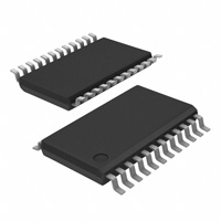
Package Information(1)
PART NUMBER
SN74LVC4245A
(1)
PACKAGE
BODY SIZE (NOM)
DB (SSOP, 24)
8.20 mm × 5.30 mm
DW (SOIC, 24)
15.40 mm × 7.50 mm
PW (TSSOP, 24)
7.80 mm × 4.40 mm
For all available packages, see the orderable addendum at
the end of the data sheet.
2
DIR
22
OE
3
A1
21
B1
To Seven Other Channels
Simplified Schematic
An IMPORTANT NOTICE at the end of this data sheet addresses availability, warranty, changes, use in safety-critical applications,
intellectual property matters and other important disclaimers. PRODUCTION DATA.
�SN74LVC4245A
www.ti.com
SCAS375J – MARCH 1994 – REVISED DECEMBER 2022
Table of Contents
1 Features............................................................................1
2 Applications..................................................................... 1
3 Description.......................................................................1
4 Revision History.............................................................. 2
5 Pin Configuration and Functions...................................3
6 Specifications.................................................................. 4
6.1 Absolute Maximum Ratings........................................ 4
6.2 Absolute Maximum Ratings........................................ 4
6.3 ESD Ratings............................................................... 4
6.4 Recommended Operating Conditions.........................5
6.5 Recommended Operating Conditions.........................5
6.6 Thermal Information....................................................5
6.7 Electrical Characteristics.............................................6
6.8 Electrical Characteristics.............................................6
6.9 Switching Characteristics............................................7
6.10 Operating Characteristics......................................... 7
6.11 Typical Characteristics.............................................. 7
7 Parameter Measurement Information............................ 8
7.1 A Port.......................................................................... 8
7.2 B Port.......................................................................... 9
8 Detailed Description......................................................10
8.1 Overview................................................................... 10
8.2 Functional Block Diagram......................................... 10
8.3 Feature Description...................................................10
8.4 Device Functional Modes..........................................10
9 Application and Implementation.................................. 11
9.1 Application Information..............................................11
9.2 Typical Application.................................................... 11
10 Power Supply Recommendations..............................13
10.1 Power-Up Consideration.........................................13
11 Layout........................................................................... 13
11.1 Layout Guidelines................................................... 13
11.2 Layout Example...................................................... 13
12 Device and Documentation Support..........................14
12.1 Documentation Support.......................................... 14
12.2 Receiving Notification of Documentation Updates..14
12.3 Support Resources................................................. 14
12.4 Trademarks............................................................. 14
12.5 Electrostatic Discharge Caution..............................14
12.6 Glossary..................................................................14
13 Mechanical, Packaging, and Orderable
Information.................................................................... 14
4 Revision History
Changes from Revision I (January 2015) to Revision J (December 2022)
Page
• Updated the numbering format for tables, figures, and cross-references throughout the document..................1
• Updated thermals for DB and PW package........................................................................................................5
Changes from Revision H (March 2005) to Revision I (January 2015)
Page
• Added Applications, Device Information table, Pin Functions table, ESD Ratings table, Thermal Information
table, Typical Characteristics, Feature Description section, Device Functional Modes, Application and
Implementation section, Power Supply Recommendations section, Layout section, Device and
Documentation Support section, and Mechanical, Packaging, and Orderable Information section................... 1
• Deleted Ordering Information table.....................................................................................................................1
2
Submit Document Feedback
Copyright © 2022 Texas Instruments Incorporated
Product Folder Links: SN74LVC4245A
�SN74LVC4245A
www.ti.com
SCAS375J – MARCH 1994 – REVISED DECEMBER 2022
5 Pin Configuration and Functions
VCCA
1
24
VCCB
DIR
2
23
NC,VCCB
A1
3
22
OE
A2
4
21
B1
A3
5
20
B2
A4
6
19
B3
A5
7
18
B4
A6
8
17
B5
A7
9
16
B6
A8
10
15
B7
GND
11
14
B8
GND
12
13
GND
Not to scale
Figure 5-1. DB, DW, or PW Package, SOP, TSSOP, (Top View)
Table 5-1. Pin Functions
PIN
NAME
NO.
TYPE(1)
DESCRIPTION
VCCA
1
—
DIR
2
I
A1
3
I/O
Transceiver I/O pin
A2
4
I/O
Transceiver I/O pin
A3
5
I/O
Transceiver I/O pin
A4
6
I/O
Transceiver I/O pin
A5
7
I/O
Transceiver I/O pin
A6
8
I/O
Transceiver I/O pin
A7
9
I/O
Transceiver I/O pin
A8
10
I/O
Transceiver I/O pin
GND
11
—
Ground
GND
12
—
Ground
GND
13
—
Ground
B8
14
I/O
Transceiver I/O pin
B7
15
I/O
Transceiver I/O pin
B6
16
I/O
Transceiver I/O pin
B5
17
I/O
Transceiver I/O pin
B4
18
I/O
Transceiver I/O pin
B3
19
I/O
Transceiver I/O pin
B2
20
I/O
Transceiver I/O pin
B1
21
I/O
Transceiver I/O pin
OE
22
I
VCCB
23
—
Power supply for side B
VCCB
24
—
Power supply for side B
(1)
Power supply for side A
Direction control
Output Enable
I = input, O = output
Submit Document Feedback
Copyright © 2022 Texas Instruments Incorporated
Product Folder Links: SN74LVC4245A
3
�SN74LVC4245A
www.ti.com
SCAS375J – MARCH 1994 – REVISED DECEMBER 2022
6 Specifications
6.1 Absolute Maximum Ratings
over operating free-air temperature range for VCCA = 4.5 V to 5.5 V (unless otherwise noted)(1)
VCCA
Supply voltage range
MAX
6.5
UNIT
V
–0.5
VCCA + 0.5
Control inputs
–0.5
6
Output voltage range
A port(2)
–0.5
VCCA + 0.5
IIK
Input clamp current
VI < 0
–50
mA
IOK
Output clamp current
VO < 0
–50
mA
IO
Continuous output current
±50
mA
±100
mA
150
°C
VI
Input voltage range
VO
A
port(2)
MIN
–0.5
Continuous current through each VCCA or GND
Tstg
(1)
(2)
Storage temperature range
–65
V
V
Stresses beyond those listed under Absolute Maximum Ratings may cause permanent damage to the device. These are stress ratings
only, and functional operation of the device at these or any other conditions beyond those indicated under Section 6.4 is not implied.
Exposure to absolute-maximum-rated conditions for extended periods may affect device reliability.
This value is limited to 6 V maximum.
6.2 Absolute Maximum Ratings
over operating free-air temperature range for VCCB = 2.7 V to 3.6 V (unless otherwise noted)(1)
MIN
VCCB
Supply voltage range
VI
Input voltage range
MAX
UNIT
–0.5
4.6
V
B port(2)
–0.5
VCCB + 0.5
V
port(2)
–0.5
VCCB + 0.5
VO
Output voltage range
B
IIK
Input clamp current
VI < 0
–50
mA
IOK
Output clamp current
VO < 0
–50
mA
IO
Continuous output current
±50
mA
±100
mA
150
°C
Continuous current through VCCB or GND
Tstg
(1)
(2)
Storage temperature range
–65
V
Stresses beyond those listed under Absolute Maximum Ratings may cause permanent damage to the device. These are stress ratings
only, and functional operation of the device at these or any other conditions beyond those indicated under Section 6.4 is not implied.
Exposure to absolute-maximum-rated conditions for extended periods may affect device reliability.
This value is limited to 4.6 V maximum.
6.3 ESD Ratings
PARAMETER
V(ESD)
(1)
(2)
4
Electrostatic
discharge
DEFINITION
Human body model (HBM), per ANSI/ESDA/JEDEC JS-001, all pins(1)
Charged device model (CDM), per JEDEC specification JESD22-C101, all
pins(2)
VALUE
UNIT
2000
V
1000
JEDEC document JEP155 states that 500-V HBM allows safe manufacturing with a standard ESD control process.
JEDEC document JEP157 states that 250-V CDM allows safe manufacturing with a standard ESD control process.
Submit Document Feedback
Copyright © 2022 Texas Instruments Incorporated
Product Folder Links: SN74LVC4245A
�SN74LVC4245A
www.ti.com
SCAS375J – MARCH 1994 – REVISED DECEMBER 2022
6.4 Recommended Operating Conditions
for VCCA = 4.5 V to 5.5 V(1)
MIN
MAX
4.5
5.5
UNIT
VCCA
Supply voltage
VIH
High-level input voltage
VIL
Low-level input voltage
0.8
V
VIA
Input voltage
0
VCCA
V
VOA
Output voltage
0
VCCA
V
IOH
High-level output current
–24
mA
IOL
Low-level output current
24
mA
TA
Operating free-air temperature
85
°C
(1)
2
–40
V
V
All unused inputs of the device must be held at the associated VCC or GND to ensure proper device operation. Refer to the TI
application report, Implications of Slow or Floating CMOS Inputs, literature number SCBA004.
6.5 Recommended Operating Conditions
for VCCB = 2.7 V to 3.6 V(1)
VCCB
Supply voltage
VIH
High-level input voltage
VCCB = 2.7 V to 3.6 V
VIL
Low-level input voltage
VCCB = 2.7 V to 3.6 V
VIB
Input voltage
VOB
Output voltage
IOH
High-level output current
IOL
Low-level output current
TA
Operating free-air temperature
(1)
MIN
MAX
2.7
3.6
2
UNIT
V
V
0.8
V
0
VCCB
V
0
VCCB
V
VCCB = 2.7 V
–12
VCCB = 3 V
–24
VCCB = 2.7 V
12
VCCB = 3 V
24
–40
85
mA
mA
°C
All unused inputs of the device must be held at the associated VCC or GND to ensure proper device operation. Refer to the TI
application report, Implications of Slow or Floating CMOS Inputs, literature number SCBA004.
6.6 Thermal Information
SN74LVC4245A
THERMAL
METRIC(1)
DB
PW
UNIT
24 PINS
RθJA
Junction-to-ambient thermal resistance
90.7
100.6
°C/W
RθJC(top)
Junction-to-case (top) thermal resistance
51.9
44.7
°C/W
RθJB
Junction-to-board thermal resistance
49.7
55.8
°C/W
ψJT
Junction-to-top characterization parameter
18.8
6.8
°C/W
ψJB
Junction-to-board characterization parameter
49.3
55.4
°C/W
(1)
For more information about traditional and new thermal metrics, see the IC Package Thermal Metrics application report, SPRA953.
Submit Document Feedback
Copyright © 2022 Texas Instruments Incorporated
Product Folder Links: SN74LVC4245A
5
�SN74LVC4245A
www.ti.com
SCAS375J – MARCH 1994 – REVISED DECEMBER 2022
6.7 Electrical Characteristics
over recommended operating free-air temperature range for VCCA = 4.5 V to 5.5 V (unless otherwise noted)(1)
PARAMETER
TEST CONDITIONS
IOH = –100 μA
VOH
IOH = –24 mA
IOL = 100 μA
VOL
IOL = 24 mA
VCCA
MIN
4.5 V
4.3
5.5 V
5.3
4.5 V
3.7
5.5 V
4.7
TYP(2) MAX
UNIT
V
4.5 V
0.2
5.5 V
0.2
4.5 V
0.55
5.5 V
0.55
V
II
Control inputs
VI = VCCA or GND
5.5 V
±1
μA
IOZ (3)
A port
VO = VCCA or GND
5.5 V
±5
μA
5.5 V
80
μA
1.5
mA
ICCA
ΔICCA
(4)
VI = VCCA or GND,
IO = 0
One input at 3.4 V,
Other inputs at VCCA or GND
5.5 V
Ci
Control inputs
VI = VCCA or GND
Open
5
pF
Cio
A port
VO = VCCA or GND
5V
11
pF
(1)
(2)
(3)
(4)
VCCB = 2.7 V to 3.6 V.
All typical values are measured at VCC = 5 V, TA = 25°C.
For I/O ports, the parameter IOZ includes the input leakage current.
This is the increase in supply current for each input that is at one of the specified TTL voltage levels, rather than 0 V or the associated
VCC.
6.8 Electrical Characteristics
over recommended operating free-air temperature range for VCCB = 2.7 V to 3.6 V (unless otherwise noted)(1)
PARAMETER
TEST CONDITIONS
IOH = –100 μA
VOH
IOZ (2)
B port
2.4
IOH = –24 mA
3V
2
IOL = 100 μA
2.7 V to 3.6 V
IOL = 12 mA
2.7 V
0.4
IOL = 24 mA
3V
0.55
VO = VCCB or GND
ΔICCB (3)
One input at VCCB – 0.6
V,
Other inputs at VCCB or GND
(4)
MAX
VO = VCCB or GND
UNIT
VCC – 0.2
2.2
IO = 0
(1)
(2)
(3)
TYP(4)
3V
VI = VCCB or GND,
B port
MIN
2.7 V
ICCB
Cio
6
2.7 V to 3.6 V
IOH = –12 mA
VOL
VCCB
V
0.2
V
3.6 V
±5
μA
3.6 V
50
μA
2.7 V to 3.6 V
0.5
mA
3.3 V
11
pF
VCCA = 5 V ± 0.5 V.
For I/O ports, the parameter IOZ includes the input leakage current.
This is the increase in supply current for each input that is at one of the specified TTL voltage levels, rather than 0 V or the associated
VCC.
All typical values are measured at VCC = 3.3 V, TA = 25°C.
Submit Document Feedback
Copyright © 2022 Texas Instruments Incorporated
Product Folder Links: SN74LVC4245A
�SN74LVC4245A
www.ti.com
SCAS375J – MARCH 1994 – REVISED DECEMBER 2022
6.9 Switching Characteristics
over recommended operating free-air temperature range, CL = 50 pF (unless otherwise noted) (see Figure 7-1 and Figure
7-2)
PARAMETER
FROM
(INPUT)
TO
(OUTPUT)
A
B
B
A
OE
A
OE
B
OE
A
OE
B
tPHL
tPLH
tPHL
tPLH
tPZL
tPZH
tPZL
tPZH
tPLZ
tPHZ
tPLZ
tPHZ
VCCA = 5 V ± 0.5 V,
VCCB = 2.7 V to 3.6 V
UNIT
MIN
MAX
1
6.3
1
6.7
1
6.1
1
5
1
9
1
10
1
10.3
1
9.8
1
7
1
5.8
1
7.7
1
7.8
ns
ns
ns
ns
ns
ns
6.10 Operating Characteristics
VCCA = 4.5 V to 5.5 V, VCCB = 2.7 V to 3.6 V, TA = 25°C
PARAMETER
Cpd
TEST CONDITIONS
Outputs enabled
Power dissipation capacitance per transceiver
CL = 0,
Outputs disabled
TYP
f = 10 MHz
39.5
5
UNIT
pF
6.11 Typical Characteristics
14
10
12
VCC = 3 V,
TA = 25°C
tpd – Propagation Delay Time – ns
tpd – Propagation Delay Time – ns
VCC = 3 V,
TA = 25°C
One Output Switching
Four Outputs Switching
Eight Outputs Switching
10
8
6
4
2
One Output Switching
Four Outputs Switching
Eight Outputs Switching
8
6
4
2
0
50
100
150
200
250
300
0
CL – Load Capacitance – pF
Figure 6-1. Propagation Delay (Low to High
Transition)
vs Load Capacitance
50
100
150
200
250
300
CL – Load Capacitance – pF
Figure 6-2. Propagation Delay (High to Low
Transition)
vs Load Capacitance
Submit Document Feedback
Copyright © 2022 Texas Instruments Incorporated
Product Folder Links: SN74LVC4245A
7
�SN74LVC4245A
www.ti.com
SCAS375J – MARCH 1994 – REVISED DECEMBER 2022
7 Parameter Measurement Information
7.1 A Port
2 × VCC
S1
500 Ω
From Output
Under Test
Open
GND
CL = 50 pF
(see Note A)
500 Ω
TEST
S1
tPLH/tPHL
tPLZ/tPZL
tPHZ/tPZH
Open
2 × VCC
GND
LOAD CIRCUIT
tw
VCC
Input
1.5 V
1.5 V
0V
VOLTAGE WAVEFORMS
PULSE DURATION
1.5 V
1.5 V
0V
tPLH
tPHL
VOH
Output
50% VCC
1.5 V
50% VCC
VOL
VOLTAGE WAVEFORMS
PROPAGATION DELAY TIMES
NONINVERTING OUTPUTS
Output
Waveform 1
S1 at 2 × VCC
(see Note B)
Output
Waveform 2
S1 at GND
(see Note B)
1.5 V
0V
tPLZ
tPZL
VCC
Input
3V
Output
Control
VCC
50% VCC
VOL + 0.3 V
VOL
tPHZ
tPZH
VOH - 0.3 V
50% VCC
VOH
≈0 V
VOLTAGE WAVEFORMS
ENABLE AND DISABLE TIMES
LOW- AND HIGH-LEVEL ENABLING
NOTES: A. CL includes probe and jig capacitance.
B. Waveform 1 is for an output with internal conditions such that the output is low, except when disabled by the output control.
Waveform 2 is for an output with internal conditions such that the output is high, except when disabled by the output control.
C. All input pulses are supplied by generators having the following characteristics: PRR≤ 10 MHz, ZO = 50 Ω, tr ≤ 2.5 ns, tf ≤ 2.5 ns.
D. The outputs are measured one at a time, with one transition per measurement.
E. All parameters and waveforms are not applicable to all devices.
Figure 7-1. Load Circuit and Voltage Waveforms
8
Submit Document Feedback
Copyright © 2022 Texas Instruments Incorporated
Product Folder Links: SN74LVC4245A
�SN74LVC4245A
www.ti.com
SCAS375J – MARCH 1994 – REVISED DECEMBER 2022
7.2 B Port
7V
S1
500 Ω
From Output
Under Test
Open
GND
CL = 50 pF
(see Note A)
500 Ω
TEST
S1
tPLH/tPHL
tPLZ/tPZL
tPHZ/tPZH
Open
7V
GND
LOAD CIRCUIT
tw
3V
Input
1.5 V
1.5 V
0V
VOLTAGE WAVEFORMS
PULSE DURATION
1.5 V
1.5 V
0V
tPLH
tPHL
VOH
Output
1.5 V
1.5 V
1.5 V
0V
tPLZ
tPZL
3V
Input
3V
Output
Control
1.5 V
VOL
VOLTAGE WAVEFORMS
PROPAGATION DELAY TIMES
NONINVERTING OUTPUTS
Output
Waveform 1
S1 at 7 V
(see Note B)
3.5 V
1.5 V
VOL
tPHZ
tPZH
Output
Waveform 2
S1 at GND
(see Note B)
VOL + 0.3 V
1.5 V
VOH - 0.3 V
VOH
≈0 V
VOLTAGE WAVEFORMS
ENABLE AND DISABLE TIMES
LOW- AND HIGH-LEVEL ENABLING
NOTES: A. CL includes probe and jig capacitance.
B. Waveform 1 is for an output with internal conditions such that the output is low, except when disabled by the output control.
Waveform 2 is for an output with internal conditions such that the output is high, except when disabled by the output control.
C. All input pulses are supplied by generators having the following characteristics: PRR≤ 10 MHz, ZO = 50 Ω, tr ≤ 2.5 ns, tf ≤ 2.5 ns.
D. The outputs are measured one at a time, with one transition per measurement.
E. All parameters and waveforms are not applicable to all devices.
Figure 7-2. Load Circuit and Voltage Waveforms
Submit Document Feedback
Copyright © 2022 Texas Instruments Incorporated
Product Folder Links: SN74LVC4245A
9
�SN74LVC4245A
www.ti.com
SCAS375J – MARCH 1994 – REVISED DECEMBER 2022
8 Detailed Description
8.1 Overview
SN74LVC4245A is an 8-bit (octal) noninverting bus transceiver contains two separate supply rails; B port has
VCCB, which is set at 3.3 V, and A port has VCCA, which is set at 5 V. This allows for translation from a 3.3-V to
a 5-V environment, and vice versa, designed for asynchronous communication between data buses. The device
transmits data from the A bus to the B bus or from the B bus to the A bus, depending on the logic level at the
direction-control (DIR) input. The output-enable ( OE) input can be used to disable the device so the buses are
effectively isolated. The control circuitry (DIR, OE) is powered by VCCA.
8.2 Functional Block Diagram
2
DIR
22
OE
3
A1
21
B1
To Seven Other Channels
8.3 Feature Description
•
•
24 mA drive at 3-V supply
– Good for heavier loads and longer traces
Low VIH
– Allows 3.3-V to 5-V translation
8.4 Device Functional Modes
Table 8-1. Function Table
INPUTS
OE
10
DIR
OPERATION
L
L
B data to A bus
L
H
A data to B bus
H
X
Isolation
Submit Document Feedback
Copyright © 2022 Texas Instruments Incorporated
Product Folder Links: SN74LVC4245A
�SN74LVC4245A
www.ti.com
SCAS375J – MARCH 1994 – REVISED DECEMBER 2022
9 Application and Implementation
Note
Information in the following applications sections is not part of the TI component specification,
and TI does not warrant its accuracy or completeness. TI’s customers are responsible for
determining suitability of components for their purposes, as well as validating and testing their design
implementation to confirm system functionality.
9.1 Application Information
The SN74LVC4245A device pinout allows the designer to switch to a normal all-3.3-V or all-5-V 20-pin
'245 device without board re-layout. The designer uses the data paths for pins 2–11 and 14–23 of the
SN74LVC4245A to align with the conventional SN74LVC4245 device's pinout. SN74LVC4245A is a high drive
CMOS device that can be used for a multitude of bus interface type applications where output drive or PCB trace
length is a concern.
9.2 Typical Application
3V
5V
VCCA
DIR
VCCB
B1
C/System
Logic/LEDs
OE
C or System
Logic
B8
A1
A8
GND
Figure 9-1. Typical Application Schematic
9.2.1 Design Requirements
This device uses CMOS technology and has balanced output drive. Care should be taken to avoid bus
contention because it can drive currents that would exceed maximum limits. The high drive will also create
fast edges into light loads so routing and load conditions should be considered to prevent ringing.
Submit Document Feedback
Copyright © 2022 Texas Instruments Incorporated
Product Folder Links: SN74LVC4245A
11
�SN74LVC4245A
www.ti.com
SCAS375J – MARCH 1994 – REVISED DECEMBER 2022
9.2.2 Detailed Design Procedure
1. Recommended Input Conditions:
• For rise time and fall time specifcations, see (Δt/ΔV) in the Section 6.4 table.
• For specified high and low levels, see (VIH and VIL) in the Section 6.4 table.
2. Recommend Output Conditions:
• Load currents should not exceed (IO max) per output and should not exceed (Continuous current through
VCC or GND) total current for the part. These limits are located in the Section 6.1 table.
• Outputs should not be pulled above VCC.
• Series resistors on the output may be used if the user desires to slow the output edge signal or limit the
output current.
9.2.3 Application Curves
60
100
TA = 25°C, VCC = 3 V,
VIH = 3 V, VIL = 0 V,
All Outputs Switching
80
TA = 25°C, VCC = 3 V,
VIH = 3 V, VIL = 0 V,
All Outputs Switching
40
20
I OH – mA
I OL – mA
60
40
0
–20
–40
20
–60
0
–80
–20
–0.2
0.0
0.2
0.4
0.6
0.8
1.0
1.2
1.4
–100
–1
–0.5 0.0
0.5
1.0
1.5
2.0
2.5
3.0
3.5
4.0
VOH – V
VOL – V
Figure 9-2. Output Drive Current (IOL)
vs LOW-level Output Voltage (VOL)
12
1.6
Figure 9-3. Output Drive Current (IOH)
vs HIGH-level Output Voltage (VOH)
Submit Document Feedback
Copyright © 2022 Texas Instruments Incorporated
Product Folder Links: SN74LVC4245A
�SN74LVC4245A
www.ti.com
SCAS375J – MARCH 1994 – REVISED DECEMBER 2022
10 Power Supply Recommendations
10.1 Power-Up Consideration
TI level-translation devices offer an opportunity for successful mixed-voltage signal design. A proper power-up
sequence always should be followed to avoid excessive supply current, bus contention, oscillations, or other
anomalies caused by improperly biased device terminals. Take these precautions to guard against such powerup problems:
1. Connect ground before any supply voltage is applied.
2. Power up the control side of the device (VCCA for all four of these devices).
3. Tie OE to VCCA with a pullup resistor so that it ramps with VCCA.
4. Depending on the direction of the data path, DIR can be high or low. If DIR high is needed (A data to B bus),
ramp it with VCCA. Otherwise, keep DIR low.
For more information, refer to the Voltage-Level-Translation Devices application note.
11 Layout
11.1 Layout Guidelines
When using multiple bit logic devices, inputs should not float. In many cases, functions or parts of functions of
digital logic devices are unused. Some examples are when only two inputs of a triple-input AND gate are used,
or when only 3 of the 4-buffer gates are used. Such input pins should not be left unconnected because the
undefined voltages at the outside connections result in undefined operational states.
Specified in Figure 11-1 are rules that must be observed under all circumstances. All unused inputs of digital
logic devices must be connected to a high or low bias to prevent them from floating. The logic level that should
be applied to any particular unused input depends on the function of the device. Generally they will be tied to
GND or VCC, whichever makes more sense or is more convenient.
11.2 Layout Example
VCC
Unused Input
Input
Output
Unused Input
Output
Input
Figure 11-1. Layout Diagram
Submit Document Feedback
Copyright © 2022 Texas Instruments Incorporated
Product Folder Links: SN74LVC4245A
13
�SN74LVC4245A
www.ti.com
SCAS375J – MARCH 1994 – REVISED DECEMBER 2022
12 Device and Documentation Support
12.1 Documentation Support
12.1.1 Related Documentation
For related documentation, see the following:
•
Texas Instruments, Voltage-Level-Translation Devices application note
12.2 Receiving Notification of Documentation Updates
To receive notification of documentation updates, navigate to the device product folder on ti.com. Click on
Subscribe to updates to register and receive a weekly digest of any product information that has changed. For
change details, review the revision history included in any revised document.
12.3 Support Resources
TI E2E™ support forums are an engineer's go-to source for fast, verified answers and design help — straight
from the experts. Search existing answers or ask your own question to get the quick design help you need.
Linked content is provided "AS IS" by the respective contributors. They do not constitute TI specifications and do
not necessarily reflect TI's views; see TI's Terms of Use.
12.4 Trademarks
TI E2E™ is a trademark of Texas Instruments.
All trademarks are the property of their respective owners.
12.5 Electrostatic Discharge Caution
This integrated circuit can be damaged by ESD. Texas Instruments recommends that all integrated circuits be handled
with appropriate precautions. Failure to observe proper handling and installation procedures can cause damage.
ESD damage can range from subtle performance degradation to complete device failure. Precision integrated circuits may
be more susceptible to damage because very small parametric changes could cause the device not to meet its published
specifications.
12.6 Glossary
TI Glossary
This glossary lists and explains terms, acronyms, and definitions.
13 Mechanical, Packaging, and Orderable Information
The following pages include mechanical, packaging, and orderable information. This information is the most
current data available for the designated devices. This data is subject to change without notice and revision of
this document. For browser-based versions of this data sheet, refer to the left-hand navigation.
14
Submit Document Feedback
Copyright © 2022 Texas Instruments Incorporated
Product Folder Links: SN74LVC4245A
�IMPORTANT NOTICE AND DISCLAIMER
TI PROVIDES TECHNICAL AND RELIABILITY DATA (INCLUDING DATA SHEETS), DESIGN RESOURCES (INCLUDING REFERENCE
DESIGNS), APPLICATION OR OTHER DESIGN ADVICE, WEB TOOLS, SAFETY INFORMATION, AND OTHER RESOURCES “AS IS”
AND WITH ALL FAULTS, AND DISCLAIMS ALL WARRANTIES, EXPRESS AND IMPLIED, INCLUDING WITHOUT LIMITATION ANY
IMPLIED WARRANTIES OF MERCHANTABILITY, FITNESS FOR A PARTICULAR PURPOSE OR NON-INFRINGEMENT OF THIRD
PARTY INTELLECTUAL PROPERTY RIGHTS.
These resources are intended for skilled developers designing with TI products. You are solely responsible for (1) selecting the appropriate
TI products for your application, (2) designing, validating and testing your application, and (3) ensuring your application meets applicable
standards, and any other safety, security, regulatory or other requirements.
These resources are subject to change without notice. TI grants you permission to use these resources only for development of an
application that uses the TI products described in the resource. Other reproduction and display of these resources is prohibited. No license
is granted to any other TI intellectual property right or to any third party intellectual property right. TI disclaims responsibility for, and you
will fully indemnify TI and its representatives against, any claims, damages, costs, losses, and liabilities arising out of your use of these
resources.
TI’s products are provided subject to TI’s Terms of Sale or other applicable terms available either on ti.com or provided in conjunction with
such TI products. TI’s provision of these resources does not expand or otherwise alter TI’s applicable warranties or warranty disclaimers for
TI products.
TI objects to and rejects any additional or different terms you may have proposed. IMPORTANT NOTICE
Mailing Address: Texas Instruments, Post Office Box 655303, Dallas, Texas 75265
Copyright © 2022, Texas Instruments Incorporated
�


 工商网监
湘ICP备2023018690号
工商网监
湘ICP备2023018690号
