Product
Folder
Order
Now
Support &
Community
Tools &
Software
Technical
Documents
SN75DP139
SLLS977F – APRIL 2009 – REVISED JULY 2017
SN75DP139 DisplayPort to TMDS Level-Shifting Re-Driver
1 Features
2 Applications
•
•
1
•
•
•
•
•
•
•
•
•
•
•
•
DisplayPort Physical Layer Input Port to TMDS
Physical Layer Output Port
Integrated TMDS Level-Shifting Re-driver With
Receiver Equalization
Supports Data Rates up to 3.4 Gbps
Achieves HDMI 1.4b Compliance
3D HDMI Support With TMDS Clock Rates up to
340 MHz
4k × 2k Operation (30 Hz, 24bpp)
Deep Color Supporting 36bpp
Integrated I2C Logic Block for DVI/HDMI
Connector Recognition
Integrated Active I2C Buffer
Enhanced ESD: 10 kV on All Pins
Enhanced Commercial Temperature Range: 0°C
to 85°C
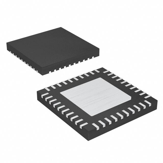
48-Pin 7-mm × 7-mm VQFN (RGZ) Package
40-Pin 5-mm × 5-mm WQFN (RSB) Package
Personal Computer Market
– DP/TMDS Dongle
– Desktop PC
– Notebook PC
– Docking Station
– Stand-Alone Video Card
3 Description
The SN75DP139 is a dual-mode DisplayPort input to
Transition-Minimized Differential Signaling (TMDS)
output. The TMDS output has a built-in level-shifting
re-driver supporting Digital Video Interface (DVI) 1.0
and High Definition Multimedia Interface (HDMI) 1.4b
standards. The SN75DP139 is specified up to a
maximum data rate of 3.4 Gbps, supporting
resolutions greater then 1920 × 1200 or HDTV 12-bit
color depth at 1080p (progressive scan). The
SN75DP139 is compliant with the HDMI 1.4b
specifications and supports optional protocol
enhancements such as 3D graphics at resolutions
demanding a pixel rate up to 340 MHz.
Device Information(1)
PART NUMBER
SN75DP139
PACKAGE
BODY SIZE (NOM)
VQFN (48)
7.00 mm x 7.00 mm
WQFN (40)
5.00 mm x 5.00 mm
(1) For all available packages, see the orderable addendum at
the end of the datasheet.
Typical Application
GPU
DP++
SN75DP139 TMDS
TMDS Buffer
Computer Notebook
Docking Station
DVI or HDMI
Compliant
Monitor or HDTV
Dongle
GPU - Graphics Processing Unit
DP++ - Dual-Mode DisplayPort
TMDS - Transition-Minimized Differential Signaling
DVI - Digital Visual Interface
HDMI - High Definition Multimedia Interface
1
An IMPORTANT NOTICE at the end of this data sheet addresses availability, warranty, changes, use in safety-critical applications,
intellectual property matters and other important disclaimers. PRODUCTION DATA.
�SN75DP139
SLLS977F – APRIL 2009 – REVISED JULY 2017
www.ti.com
Table of Contents
1
2
3
4
5
6
Features ..................................................................
Applications ...........................................................
Description .............................................................
Revision History.....................................................
Pin Configuration and Functions .........................
Specifications.........................................................
1
1
1
2
4
7
6.1
6.2
6.3
6.4
6.5
6.6
6.7
6.8
Absolute Maximum Ratings ...................................... 7
ESD Ratings.............................................................. 7
Recommended Operating Conditions....................... 7
Thermal Information .................................................. 8
Electrical Characteristics (Device Power) ................. 9
Electrical Characteristics (Hot Plug Detect) .............. 9
Electrical Characteristics (Aux / I2C Pins)................. 9
Electrical Characteristics (TMDS and Main Link
Pins) ......................................................................... 10
6.9 Switching Characteristics (Hot Plug Detect) ........... 11
6.10 Switching Characteristics (Aux / I2C Pins) ............ 12
6.11 Switching Characteristics (TMDS and Main Link
Pins) ......................................................................... 14
6.12 Typical Characteristics .......................................... 17
7
7.1
7.2
7.3
7.4
7.5
8
Overview .................................................................
Functional Block Diagram .......................................
Feature Description.................................................
Device Functional Modes........................................
Programming...........................................................
18
18
19
22
22
Application and Implementation ........................ 27
8.1 Application Information............................................ 27
8.2 Typical Application .................................................. 27
9 Power Supply Recommendations...................... 29
10 Layout................................................................... 29
10.1 Layout Guidelines ................................................. 29
10.2 Layout Example .................................................... 30
11 Device and Documentation Support ................. 32
11.1
11.2
11.3
11.4
11.5
Receiving Notification of Documentation Updates
Community Resources..........................................
Trademarks ...........................................................
Electrostatic Discharge Caution ............................
Glossary ................................................................
32
32
32
32
32
12 Mechanical, Packaging, and Orderable
Information ........................................................... 32
Detailed Description ............................................ 18
4 Revision History
NOTE: Page numbers for previous revisions may differ from page numbers in the current version.
Changes from Revision E (September 2014) to Revision F
Page
•
Added Note 1 to the Pin Functions table................................................................................................................................ 5
•
Changed the Handling Ratings To ESD Ratings and moved the Storage temperature range to the Absolute
Maximum Ratings ................................................................................................................................................................... 7
Changes from Revision D (July 2013) to Revision E
•
Page
Added Pin Configuration and Functions section, Handling Rating table, Feature Description section, Device
Functional Modes, Application and Implementation section, Power Supply Recommendations section, Layout
section, Device and Documentation Support section, and Mechanical, Packaging, and Orderable Information
section ................................................................................................................................................................................... 1
Changes from Revision C (December 2012) to Revision D
Page
•
Changed title and Feature bullet from "...TMDS Translator...." to "...TMDS Level Shifting Re-driver" .................................. 1
•
Changed second sentence text string in Description section from "...built in level translator..." to "built in level
shifting re-driver....."................................................................................................................................................................ 1
2
Submit Documentation Feedback
Copyright © 2009–2017, Texas Instruments Incorporated
Product Folder Links: SN75DP139
�SN75DP139
www.ti.com
SLLS977F – APRIL 2009 – REVISED JULY 2017
Changes from Revision A (July 2010) to Revision B
Page
•
Added to FEATURES "40 Pin 5 x 5 QFN (RSB) Package".................................................................................................... 1
•
Added RSB package drawing................................................................................................................................................. 4
•
Changed Pin Functions to include RSB package pins ........................................................................................................... 5
•
Added RSB package to ORDERING INFORMATION table................................................................................................... 6
•
Changed voltage range section of Absolute Maximum Ratings............................................................................................. 7
•
Changed input voltages within the Recommended Operating Conditions ............................................................................. 7
•
Changed thermal resistance info and enable voltages to 3.6V.............................................................................................. 8
•
Changed enable voltages from 5 V to 3.6 V .......................................................................................................................... 9
•
Changed VIH(AUX) max from 5.5 V to 3.6 V ............................................................................................................................. 9
•
Changed OUT_Dx terminal connections .............................................................................................................................. 18
Submit Documentation Feedback
Copyright © 2009–2017, Texas Instruments Incorporated
Product Folder Links: SN75DP139
3
�SN75DP139
SLLS977F – APRIL 2009 – REVISED JULY 2017
www.ti.com
5 Pin Configuration and Functions
21
OUT_D1-
41
42
GND
43
18
GND
IN_D3-
44
17
4
8
9 10 11 12
SRC
I2C_EN
G ND
Vsadj
HPD_SOURCE
SDA_SOURCE
SCL_SOURCE
OUT_D3+
OUT_D4+
OUT_D3-
VCC
OUT_D2+
OUT_D4-
VCC
OUT_D2-
OUT_D1+
NC
VCC
32
19
VCC
SCL_SINK
33
18
SCL_SOURCE
SDA_SINK
34
17
SDA_SOURCE
HPD_SINK
35
16
HPD_SOURCE
DDC_EN
OUT_D2-
36
15
Vsadj
37
14
I2C_EN
OUT_D3-
HPDINV
38
13
SRC
16
OUT_D3+
OVS
39
12
VCC
15
VCC
NC
40
11
NC
OUT_D2+
14
OUT_D4-
13
OUT_D4+
1
2
3
4
5
6
7
8
9
10
IN_D4+
7
20
VCC
6
21
IN_D4-
5
22
IN_D3+
4
VCC
3
23
GND
2
NC
1
VCC
48
GND
IN_D4+
24
IN_D3-
47
25
IN_D2+
46
26
VCC
VCC
IN_D4-
27
VCC
19
45
28
VCC
IN_D2+
IN_D3+
29
31
OUT_D1+
IN_D2-
20
OUT_D1-
OE_N
VCC
SCL_SINK
G ND
HPD_SINK
SDA_SINK
G ND
DDC_EN
40
GND
30
OE_N
IN_D2-
VCC
36 35 34 33 32 31 30 29 28 27 26 25
37
24
38
23
39
22
IN_D1+
IN_D1+
40-Pin WQFN
RSB Package
(Top View)
IN_D1-
IN_D1-
VCC
OVS
GND
GND
HPDINV
48-Pin VQFN
RGZ Package
(Top View)
Submit Documentation Feedback
Copyright © 2009–2017, Texas Instruments Incorporated
Product Folder Links: SN75DP139
�SN75DP139
www.ti.com
SLLS977F – APRIL 2009 – REVISED JULY 2017
Pin Functions
PIN
NO.
SIGNAL
I/O
DESCRIPTION
RGZ
RSB
IN_D1
38, 39
1, 2
I
DisplayPort Main Link Channel 0 Differential Input
IN_D2
41, 42
4, 5
I
DisplayPort Main Link Channel 1 Differential Input
IN_D3
44, 45
6, 7
I
DisplayPort Main Link Channel 2 Differential Input
IN_D4
47, 48
9, 10
I
DisplayPort Main Link Channel 3 Differential Input
MAIN LINK INPUT PINS
MAIN LINK PORT B OUTPUT PINS
OUT_D1
23, 22
30, 29
O
TMDS Data 2 Differential Output
OUT_D2
20, 19
27, 26
O
TMDS Data 1 Differential Output
OUT_D3
17, 16
25, 24
O
TMDS Data 0 Differential Output
OUT_D4
14, 13
22, 21
O
TMDS Data Clock Differential Output
HOT PLUG DETECT PINS
HPD_SOURCE
7
16
O
Hot Plug Detect Output
HPD_SINK
30
35
I
Hot Plug Detect Input
8, 9
17, 18
I/O
Source Side Bidirectional DisplayPort Auxiliary Data Line
29, 28
34, 33
I/O
TMDS Port Bidirectional DDC Data Lines
OE_N
25
31
I
NC
10
11, 20, 40
OVS
35
39
I
DDC I2C buffer offset select
DDC_EN
32
36
I
Enables or Disables the DDC I2C buffer
HPDINV
34
38
I
HPD_SOURCE Logic and Level Select
VSadj
6
15
I
TMDS Compliant Voltage Swing Control
SRC
3
13
I
TMDS outputs rise and fall time select
I2C_EN
4
14
I
Internal I2C register enable, used for HDMI / DVI connector differentiation
AUXILIARY DATA PINS
SDA_SOURCE,
SCL_SOURCE
SDA_SINK,
SCL_SINK
CONTROL PINS
Output Enable and power saving function for High Speed Differential level
shifter path.
No Connect
SUPPLY AND GROUND PINS
VCC
2, 11, 15, 21, 26,
33, 40, 46
3, 8, 12, 19, 23
28, 32, 37
GND
1, 5, 12, 18, 24,
27, 31, 36, 37,
43 (1)
Thermal Pad
(1)
3.3 V Supply
Ground
Connect the Thermal Pad to GND
Submit Documentation Feedback
Copyright © 2009–2017, Texas Instruments Incorporated
Product Folder Links: SN75DP139
5
�SN75DP139
SLLS977F – APRIL 2009 – REVISED JULY 2017
www.ti.com
Table 1. Control Pin Lookup Table
SIGNAL
OE_N
I2C_EN
VSadj
HPDINV
SRC
OVS
DDC_EN
(1)
6
LEVEL
(1)
STATE
DESCRIPTION
H
Power Saving
Mode
Main Link is disabled. IN_Dx termination = 50 Ω with common mode voltage set to
0V.
OUT_Dx outputs = high impedance
L
Normal Mode
IN_Dx termination = 50 Ω
OUT_Dx outputs = active
H
HDMI
L
DVI
4.02 kΩ
±5%
Output Voltage
Swing Contol
Driver output voltage swing precision control to aid with system compliance
H
HPD Inversion
HPD_SOURCE VOH =0.9V (typical) and HPD logic is inverted
L
HPD noninversion
H
Edge Rate:
Slowest
SRC helps to slow down the rise and fall time. SRC =High adds ~60ps to the rise
and fall time of the TMDS differential output signals in addition to the I2C_EN pin
selection (recommended setting)
L
Edge Rate: Slow
SRC helps to slow down the rise and fall time. SRC =Low adds ~30ps to the rise
and fall time of the TMDS differential output signals in addition to the I2C_EN pin
selection
Hi-Z
Edge Rate
Leaving the SRC pin High Z, will keep the default rise and fall time of the TMDS
differential output signals as selected by the I2C_EN pin.
It is recommended that an external resistor-divider (less than 100 kΩ) is used so
that voltage on this pin = VCC/2, if Hi-Z logic level is intended on this pin.
H
Offset 1
DDC source side VOL and VIL offset range 1
The Internal I2C register is active and readable when the TMDS port is selected
indicating that the connector being used is HDMI.
This mode selects the fastest rise and fall time for the TMDS differential output
signals
The Internal I2C register is disabled and not readable when the TMDS port is
selected indicating that the connector being used is DVI.
This mode selects a slower rise and fall time for the TMDS differential output signals
See Application Information.
HPD_SOURCE VOH =3.2V (typical) and HPD logic is non-inverted
L
Offset 2
DDC source side VOL and VIL offset range 2
Hi-Z
Offset 3
DDC source side VOL and VIL offset range 3
It is recommended that an external resistor-divider (less than 100 kΩ) is used so
that voltage on this pin = VCC/2, if Hi-Z logic level is intended on this pin.
H
DDC Buffer
enabled
DDC Buffer is enabled
L
DDC buffer
disabled
DDC Buffer is disabled
(H) Logic High; (L) Logic Low; (Z) High Z
Submit Documentation Feedback
Copyright © 2009–2017, Texas Instruments Incorporated
Product Folder Links: SN75DP139
�SN75DP139
www.ti.com
SLLS977F – APRIL 2009 – REVISED JULY 2017
6 Specifications
6.1 Absolute Maximum Ratings
over operating free-air temperature range (unless otherwise noted) (1)
MIN
MAX
UNIT
–0.3
3.6
V
Main Link Input (IN_Dx) differential voltage
–0.3
VCC + 0.3
V
TMDS Outputs (OUT_Dx)
–0.3
VCC + 0.3
HPD_SOURCE, SDA_SOURCE, SCL_SOURCE, OVS, DDC_EN, VSadj,
SRC, I2C_EN
–0.3
VCC + 0.3
HPD_SINK, SDA_SINK, SCL_SINK, OE_EN, HPDINV
–0.3
5.5
–55
150
Supply voltage range (2) VCC
Voltage range
Storage temperature range, Tstg
(1)
(2)
°C
Stresses beyond those listed under Absolute Maximum Ratings may cause permanent damage to the device. These are stress ratings
only and functional operation of the device at these or any conditions beyond those indicated under Recommended Operating
Conditions is not implied. Exposure to absolute-maximum-rated conditions for extended periods may affect device reliability.
All voltage values, except differential voltages, are with respect to network ground terminal.
6.2 ESD Ratings
VALUE
V(ESD)
(1)
(2)
(3)
Electrostatic discharge
Human body model (1)
±10000
Charged-device model (2)
±1500
Machine model (3)
±200
UNIT
V
V
Tested in accordance with JEDEC Standard 22, Test Method A114-B
Tested in accordance with JEDEC Standard 22, Test Method C101-A
Tested in accordance with JEDEC Standard 22, Test Method A115-A
6.3 Recommended Operating Conditions
over operating free-air temperature range (unless otherwise noted)
MIN NOM MAX
VCC
Supply Voltage
3
TA
Operating free-air temperature
3.3
UNIT
3.6
V
0
85
°C
V
MAIN LINK DIFFERENTIAL INPUT PINS
VID_PP
Peak-to-peak AC input differential voltage
dR
Data rate
trise fall time
Input Signal Rise and Fall time (20%-80%)
VPRE
Pre-emphasis on the Input Signal at IN_Dx pins
0.15
1.2
RGZ package
0.25
3.4
RSB package
0.25
3.4
75
Gbps
ps
0
0
0
db
3
3.3
3.6
V
TMDS DIFFERENTIAL OUTPUT PINS
AVCC
TMDS output termination voltage
dR
Data rate
RT
Termination resistance
RVsadj
TMDS output swing voltage bias resistor (1)
RGZ package
0.25
3.4
RSB package
0.25
3.4
45
50
3.65
4.02
55
Gbps
Ω
kΩ
AUXILIARY AND I2C PINS
VI
Input voltage
dR(I2C)
I2C data rate
(1)
SDA_SINK, SCL_SINK
0
SDA_SOURCE, SCL_SOURCE
5.5
3.6
100
V
kHz
RVsadj resistor controls the SN75DP139 Driver output voltage swing and thus helps in meeting system compliance. It is recommended
that RVsadj resistor should be above the MIN value as indicated in the RECOMMENDED OPERATING CONDITIONS table, however for
NOM and MAX value, Figure 19 could be used as reference. It is important to note that system level losses, AVCC and RT variation
affect RVsadj resistor selection. Worse case variation on system level losses, AVCC, RT could make RVsadj resistor value of 4.02 kΩ ±5%
result in non-compliant TMDS output voltage swing. In such cases Figure 19 could be used as reference.
Submit Documentation Feedback
Copyright © 2009–2017, Texas Instruments Incorporated
Product Folder Links: SN75DP139
7
�SN75DP139
SLLS977F – APRIL 2009 – REVISED JULY 2017
www.ti.com
Recommended Operating Conditions (continued)
over operating free-air temperature range (unless otherwise noted)
MIN NOM MAX
UNIT
HPD_SINK, HPDINV, OE_N
VIH
High-level input voltage
2
5.5
V
VIL
Low-level input voltage
0
0.8
V
VIH
High-level input voltage
2
3.6
V
VIL
Low-level input voltage
0
0.8
V
VIH_SRC_OVS
High-level input voltage
3
3.6
V
VIL_SRC_OVS
Low-level input voltage
0
0.5
V
DDC_EN, I2C_EN
SRC, OVS
6.4 Thermal Information
over operating free-air temperature range (unless otherwise noted)
PARAMETER
TEST CONDITIONS
MIN
TYP
UNIT
θJB
Junction-to-board thermal
resistance
RSB package
10.8
θJCT
Junction-to-case-top thermal
resistance
RGZ package
22.5
RSB package
24.4
ψJB
Junction-to-board thermal
resistance metric
High-K board (2)
RGZ package
10.9
RSB package
10.8
ψJT
Junction-to-top thermal resistance
metric
High-K board (2)
RGZ package
0.5
RSB package
0.4
PD1
Device power dissipation (3)
HDMI Mode: OE_N = 0V, DDC_EN = 3.6V, VCC = 3.6V,
ML: VID_PP = 1200mV, 3Gbps TMDS pattern
AUX: VI = 3.3V, 100 kHz PRBS
HPD: HPD_SINK = 5V, I2C_EN = 3.6V, SRC = Hi-Z
270+146
396+146
mW
PD2
Device power dissipation (3)
DVI Mode: OE_N = 0V, DDC_EN = 3.6V, VCC = 3.6V,
ML: VID_PP = 1200mV, 3Gbps TMDS pattern
AUX: VI = 3.3V, 100 kHz PRBS
HPD: HPD_SINK= 5V, I2C_EN = 0V, SRC = Hi-Z
214+146
306+146
mW
PSD1
Device power dissipation under low
power with
HPDINV = LOW
OE_N = 5V, DDC_EN = 0V, HPDINV = 0V,
HPD_SINK = 0V
18
54
μW
PSD2
Device power dissipation under low
power with
HPDINV =HIGH
OE_N = 5V, DDC_EN = 0V, HPDINV = 5V
1.7
3
mW
PSD3
Device power dissipation under low
power with DDC enabled with
HPDINV = HIGH
OE_N = 5V, DDC_EN = 3.6V, HPDINV = 5V
16.5
29
mW
PSD4
Device power dissipation under low
power with DDC enabled with
HPDINV = LOW
OE_N = 5V, DDC_EN = 3.6V, HPDINV = 0V
15
26
mW
(1)
(2)
(3)
8
10.9
MAX (1)
RGZ package
°C/W
°C/W
°C/W
°C/W
The maximum rating is simulated under 3.6V VCC unless otherwise noted.
Test conditions for ψJB and ψJT are clarified in TI document Semiconductpr and IC Package Thermal Metrics, .
Power dissipation is the sum of the power consumption from the VCC pins, plus the 146 mW of power from the AVCC (HDMI/DVI
Receiver Termination Supply).
Submit Documentation Feedback
Copyright © 2009–2017, Texas Instruments Incorporated
Product Folder Links: SN75DP139
�SN75DP139
www.ti.com
SLLS977F – APRIL 2009 – REVISED JULY 2017
6.5 Electrical Characteristics (Device Power)
over operating free-air temperature range (unless otherwise noted)
PARAMETER
TEST CONDITIONS
MIN
TYP
MAX
UNIT
ICC1
Supply current (HDMI Mode)
HDMI Mode: OE_N = 0V, DDC_EN = 3.6 V,
VCC = 3.6 V,
ML: VID_PP = 1200 mV, 3 Gbps TMDS pattern
AUX: VI = 3.3 V, 100 kHz PRBS
HPD: HPD_SINK = 5 V, I2C_EN = 3.6 V, SRC = HiZ
82
110
mA
ICC2
Supply Current (DVI Mode)
DVI Mode: OE_N = 0V, DDC_EN = 3.6 V,
VCC = 3.6 V,
ML: VID_PP = 1200 mV, 3 Gbps TMDS pattern
AUX: VI = 3.3 V, 100 kHz PRBS
HPD: HPD_SINK= 5 V, I2C_EN = 0 V, SRC = Hi-Z
65
85
mA
ISD1
Shutdown current with
HPDINV = LOW
OE_N = 5 V, DDC_EN = 0 V, HPDINV = 0 V,
HPD_SINK = 0 V
5.5
15
μA
ISD2
Shutdown current with
HPDINV = HIGH
OE_N = 5 V, DDC_EN = 0 V, HPDINV = 5 V
0.5
0.8
mA
ISD3
Shutdown current with DDC enabled
with
HPDINV = HIGH
5
8
mA
OE_N = 5 V, DDC_EN = 3.6 V, HPDINV = 5 V
Shutdown current with DDC enabled
with
HPDINV = LOW
4.5
7.2
mA
OE_N = 5 V, DDC_EN = 3.6 V, HPDINV = 0 V
TYP
MAX
UNIT
ISD4
6.6 Electrical Characteristics (Hot Plug Detect)
over recommended operating conditions (unless otherwise noted)
PARAMETER
TEST CONDITIONS
MIN
VOH3.3
High-level output voltage
IOH = –100 μA, VCC = 3.3 V ±10%,
HPDINV = LOW
2.8
3.6
V
VOH1.1
High-level output voltage
IOH = –100 μA, VCC = 3.3 V ±10%,
HPDINV = HIGH
0.8
1.1
V
VOL
Low-level output voltage
IOH = 100 μA
0
0.1
V
IIH
High-level input current
VIH = 2.0 V, VCC = 3.6 V
–30
30
μA
IIL
Low-level input current
VIL = 0.8 V, VCC = 3.6 V
–30
30
μA
RINTHPD
Input pull down on HPD_SINK (HPD Input)
160
kΩ
110
130
MIN
TYP
6.7 Electrical Characteristics (Aux / I2C Pins)
over recommended operating conditions (unless otherwise noted)
PARAMETER
IL
TEST CONDITIONS
Low input current
2
MAX
UNIT
VCC = 3.6 V, VI = 0 V
–10
10
μA
–10
10
μA
15
pF
1.6
3.6
V
–0.2
0.36
V
0.6
0.7
V
Ilkg(AUX)
Input leakage current
AUX_I C pins
(SCL_SOURCE,
SDA_SOURCE)
VCC = 3.6V, VI = 3.6 V
CIO(AUX)
Input/Output capacitance
AUX_I2C pins
(SCL_SOURCE,
SDA_SOURCE)
DC bias = 1.65 V, AC = 2.1Vp-p,
f = 100 kHz
VIH(AUX)
High-level input voltage
AUX_I2C pins
(SCL_SOURCE,
SDA_SOURCE)
VIL1(AUX)
Low-level input voltage
AUX_I2C pins
(SCL_SOURCE,
SDA_SOURCE)
OVS = HIGH
VOL1(AUX)
Low-level output voltage
AUX_I2C pins
(SCL_SOURCE,
SDA_SOURCE)
IO = 3 mA, OVS = HIGH
Submit Documentation Feedback
Copyright © 2009–2017, Texas Instruments Incorporated
Product Folder Links: SN75DP139
9
�SN75DP139
SLLS977F – APRIL 2009 – REVISED JULY 2017
www.ti.com
Electrical Characteristics (Aux / I2C Pins) (continued)
over recommended operating conditions (unless otherwise noted)
PARAMETER
TEST CONDITIONS
2
MIN
TYP
MAX
UNIT
–0.2
0.36
V
0.5
0.6
V
–0.2
0.27
V
VIL2(AUX)
Low-level input voltage
AUX_I C pins
(SCL_SOURCE,
SDA_SOURCE)
OVS = Hi-Z
VOL2(AUX)
Low-level output voltage
AUX_I2C pins
(SCL_SOURCE,
SDA_SOURCE)
IO = 3 mA, OVS = Hi-Z
VIL3(AUX)
Low-level input voltage
AUX_I2C pins
(SCL_SOURCE,
SDA_SOURCE)
OVS = Low
VOL3(AUX)
Low-level output voltage
AUX_I2C pins
(SCL_SOURCE,
SDA_SOURCE)
IO = 3 mA, OVS = Low
0.4
0.5
V
Ilkg(I2C)
Input leakage current
I2C SDA/SCL pins
(SCL_SINK,
SDA_SINK)
VCC = 3.6 V, VI = 4.95 V
–10
10
μA
CIO(I2C)
Input/Output capacitance
I2C SDA/SCL pins
(SCL_SINK,
SDA_SINK)
DC bias = 2.5 V, AC = 3.5Vp-p, f
= 100 kHz
15
pF
VIH(I2C)
High-level input voltage
I2C SDA/SCL pins
(SCL_SINK,
SDA_SINK)
2.1
5.5
V
VIL(I2C)
Low-level input voltage
I2C SDA/SCL pins
(SCL_SINK,
SDA_SINK)
–0.2
1.5
V
VOL(I2C)
Low-level output voltage
I2C SDA/SCL pins
(SCL_SINK,
SDA_SINK)
0.2
V
IO = 3mA
6.8 Electrical Characteristics (TMDS and Main Link Pins)
over recommended operating conditions (unless otherwise noted)
PARAMETER
TEST CONDITIONS
AVCC = 3.3 V, RT = 50 Ω,
VOH
Single-ended HIGH level output voltage
VOL
Single-ended LOW level output voltage
VSWING
Single-ended output voltage swing
VOC(SS)
Change in steady-state common-mode
output voltage between logic states
VOD(PP)
Peak-to-Peak output differential voltage
V(O)SBY
Single-ended standby output voltage
AVCC = 3.3 V, RT = 50 Ω, OE_N =
High
I(O)OFF
Single-ended power down output
current
IOS
Short circuit output current
RINT
Input termination impedance
Vterm
Input termination voltage
10
MIN
TYP
MAX
UNIT
AVCC–10
AVCC+10
mV
AVCC–600
AVCC-400
mV
400
600
mV
–5
5
mV
800
1200
mV
AVCC–10
AVCC+10
mV
0V ≤ VCC ≤ 1.5 V, AVCC = 3.3 V,
RT = 50Ω
–10
10
μA
See Figure 14
–15
15
mA
60
Ω
2
V
40
1
Submit Documentation Feedback
50
Copyright © 2009–2017, Texas Instruments Incorporated
Product Folder Links: SN75DP139
�SN75DP139
www.ti.com
SLLS977F – APRIL 2009 – REVISED JULY 2017
6.9 Switching Characteristics (Hot Plug Detect)
over recommended operating conditions (unless otherwise noted)
PARAMETER
tPD(HPD)
TEST CONDITIONS
Propagation delay
HPD Input/HPD_sink
Dp139
MIN
VCC = 3.6 V
MAX
2
UNIT
30
ns
1.1 V
HPD Output/HPD_source
10 kW
HPD Input/HPD_sink
DP139
100 kW
130 kW
TYP
130 kW
100 kW
HPD Output/HPD_source
130 kW Pull down
resistor on the sink side
is integrated
130 kW Pull down
resistor is integrated
Figure 1. HPD Test Circuit (HPDINV = LOW)
Figure 2. HPD Test Circuit (VOH = 1.1),
HPDINV = HIGH
5V
HPD_SINK
50%
0V
tPD(HPD)
VCC
HPD_SOURCE
50%
0V
Figure 3. HPD Timing Diagram (HPDINV = LOW)
5V
HPD_SINK
50%
0V
tPD(HPD)
1.1 V
50%
HPD_SOURCE
0V
Figure 4. HPD Timing Diagram (HPDINV = HIGH)
Submit Documentation Feedback
Copyright © 2009–2017, Texas Instruments Incorporated
Product Folder Links: SN75DP139
11
�SN75DP139
SLLS977F – APRIL 2009 – REVISED JULY 2017
www.ti.com
6.10 Switching Characteristics (Aux / I2C Pins)
over recommended operating conditions (unless otherwise noted)
PARAMETER
TEST CONDITIONS
MIN
TYP
MAX
UNIT
tPLH1
Propagation delay time, low to high
Source to Sink
204
600
ns
tPHL1
Propagation delay time, high to low
Source to Sink
35
200
ns
tPLH2
Propagation delay time, low to high
Sink to Source
80
251
ns
tPHL2
Propagation delay time, high to low
Sink to Source
35
200
ns
tf1
Output signal fall time
Sink Side
20
72
ns
tf2
Output signal fall time
Source Side
20
72
ns
fSCL
SCL clock frequency for internal register
Source Side
100
kHz
tW(L)
Clock LOW period for I2C register
Source Side
4.7
μs
tW(H)
Clock HIGH period for internal register
Source Side
4.0
μs
tSU1
Internal register setup time, SDA to SCL
Source Side
250
ns
th(1)
Internal register hold time, SCL to SDA
Source Side
0
μs
T(buf)
Internal register bus free time between STOP and START
Source Side
4.7
μs
tsu(2)
Internal register setup time, SCL to START
Source Side
4.7
μs
th(2)
Internal register hold time, START to SCL
Source Side
4.0
μs
tsu(3)
Internal register hold time, SCL to STOP
Source Side
4.0
μs
3.3 V
VCC
R L = 2 kW
PULSE
GENERATOR
D.U.T.
CL = 100 pF
RT
VIN
VOUT
Figure 5. Source Side Test Circuit (SCL_SOURCE, SDA_SOURCE)
5V
VCC
R L = 2 kW
PULSE
GENERATOR
D.U.T.
CL = 400 pF
RT
VIN
VOUT
Figure 6. Sink Side Test Circuit (SCL_SINK,SDA_SINK)
12
Submit Documentation Feedback
Copyright © 2009–2017, Texas Instruments Incorporated
Product Folder Links: SN75DP139
�SN75DP139
www.ti.com
SLLS977F – APRIL 2009 – REVISED JULY 2017
5V
SCL_SINK
SDA_SINK
Input
1.6 V
0.1 V
tPHL2
tPLH2
3.3 V
80%
SCL_SOURCE
SDA_SOURCE
Output
1.6 V
20%
VOL
tf2
Figure 7. Source Side Output AC Measurements
3.3 V
SCL_SOURCE
SDA_SOURCE
Input
1.6 V
0.1 V
tPHL1
5V
80%
SCL_SINK
SDA_SINK
Output
1.6 V
20%
VOL
tf1
Figure 8. Sink Side Output AC Measurements
3.3 V
SCL_SOURCE
SDA_SOURCE
Input
VOL
tPLH1
SCL_SINK
SDA_SINK
Output
5V
1.6 V
Figure 9. Sink Side Output AC Measurements Continued
Submit Documentation Feedback
Copyright © 2009–2017, Texas Instruments Incorporated
Product Folder Links: SN75DP139
13
�SN75DP139
SLLS977F – APRIL 2009 – REVISED JULY 2017
www.ti.com
6.11 Switching Characteristics (TMDS and Main Link Pins)
over recommended operating conditions (unless otherwise noted)
PARAMETER
TEST CONDITIONS
MIN
TYP
MAX
UNIT
tPLH
Propagation delay time
250
350
600
ps
tPHL
Propagation delay time
250
350
600
ps
tR1
Rise Time (I2C_EN = HI, SRC = Hi-Z)
60
85
120
ps
tF1
Fall Time (I2C_EN = HI, SRC = Hi-Z)
60
85
120
ps
tR2
Rise Time (I2C_EN = Low, SRC = Hi-Z)
115
150
ps
tF2
Fall Time (I2C_EN = Low, SRC = Hi-Z)
115
150
ps
tR3
Rise Time (I2C_EN = HI, SRC = HI)
150
180
ps
tF3
Fall Time (I2C_EN = HI, SRC = HI)
150
180
ps
tR4
Rise Time (I2C_EN = HI, SRC = Low)
115
150
ps
tF4
Fall Time (I2C_EN = HI, SRC = Low)
115
150
ps
tR5
Rise Time (I2C_EN = Low, SRC = HI)
175
220
ps
tF5
Fall Time (I2C_EN = Low, SRC = HI)
175
220
ps
tR6
Rise Time (I2C_EN = Low, SRC = Low)
150
180
ps
tF6
Fall Time (I2C_EN = Low, SRC = Low)
150
180
ps
tSK(P)
Pulse skew
8
15
ps
tSK(D)
Intra-pair skew
20
65
ps
tSK(O)
Inter-pair skew
20
100
ps
tJITD(PP)
Peak-to-peak output residual data jitter
AVCC = 3.3 V, RT = 50Ω, dR = 3Gbps,
TMDS output slew rate (default).
RVsadj = 4.02 kΩ (refer to Figure 13)
14
50
ps
tJITC(PP)
Peak-to-peak output residual clock jitter
AVCC = 3.3 V, RT = 50Ω, f = 300 MHz
TMDS output slew rate (default).
RVsadj= 4.02 kΩ (refer to Figure 13)
8
30
ps
AVCC=3.3 V, RT = 50 Ω, f = 1MHz,
RVsadj = 4.02 kΩ
VTERM
3.3V
50 Ω
50 Ω
50 Ω
50 Ω
0.5 pF
D+
VD+
Receiver
VID
DV D-
VID = VD+ - VDVICM = (VD+ + VD-)
2
Y
Driver
VY
Z
VOD = VY - VZ
VOC = (VY + VZ)
VZ
2
Figure 10. TMDS Main Link Test Circuit
14
Submit Documentation Feedback
Copyright © 2009–2017, Texas Instruments Incorporated
Product Folder Links: SN75DP139
�SN75DP139
www.ti.com
SLLS977F – APRIL 2009 – REVISED JULY 2017
2.2 V
VTERM
VID
1.8 V
VID+
VID(pp)
0V
tPHL
VID-
tPLH
80%
VOD(pp)
80%
0V
20%
VOD
20%
tr
tf
Figure 11. TMDS Main Link Timing Measurements
VOC
ΔVOC (SS)
Figure 12. TMDS Main Link Common Mode Measurements
Avcc (4)
(8)
RT
Data +
Parallel
BERT
Data -
Coax
Coax
SMA
Clk -
RX
+EQ
SMA
600, 800 mV
VPP Differential
[No Pre-emphasis]
Clk +
SMA
(1)
FR 4 PCB trace
&
AC coupling Caps
Coax
Coax
SMA
SN 75 DP 139
Coax
Coax
FR 4 PCB trace
AVcc
RT
SMA
RX
+EQ
TTP 2
Jitter Test
Instrument (2,3)
RT
Coax
OUT
SMA
Coax
(6) (7)
TTP 1
(5)
OUT
SMA
SMA
RT
Jitter Test
Instrument (2,3)
TTP 3
TTP 4
1. The FR4 trace between TTP1 and TTP2 is designed to emulate 1-8" of FR4, AC coupling cap, connector and another 1-8" of FR4. Trace width - 4 mils.
-9
2. All Jitter is measured at a BER of 10
3. Residual jitter reflects the total jitter measured at TTP4 minus the jitter measured at TTP1
4. AVCC = 3.3V
5. RT = 50Ω,
6. Jitter data is taken with SN75DP139 configured in the fastest slew rate setting(default)
7. Rvsadj = 4.02kΩ
8. The input signal from parallel BERT does not have any pre-emphasis. Refer to recommended operating conditions
Figure 13. TMDS Jitter Measurements
Submit Documentation Feedback
Copyright © 2009–2017, Texas Instruments Incorporated
Product Folder Links: SN75DP139
15
�SN75DP139
SLLS977F – APRIL 2009 – REVISED JULY 2017
www.ti.com
50 W
I OS
Driver
50 W
+ 0 V or 3.6 V
-
Figure 14. TMDS Main Link Short Circuit Output Circuit
16
Submit Documentation Feedback
Copyright © 2009–2017, Texas Instruments Incorporated
Product Folder Links: SN75DP139
�SN75DP139
www.ti.com
SLLS977F – APRIL 2009 – REVISED JULY 2017
6.12 Typical Characteristics
AVCC = 3.3 V, RT = 50 Ω
50
420
45
Peak-to-Peak Residual Data Jitter (ps)
430
410
Power (mW)
400
0ƒC
0ƒC Slowest Edge Rate
390
25ƒC
25ƒC Slowest Edge Rate
380
85ƒC
85ƒC Slowest Edge Rate
370
360
40
35
0ƒC
0ƒC Slowest Edge Rate
30
25ƒC
25ƒC Slowest Edge Rate
85ƒC
25
85ƒC Slowest Edge Rate
20
15
350
340
10
0.5
1.0
1.5
2.0
2.5
3.0
3.0
3.5
3.3
Data Rate (Gbps)
3.6
Supply Voltage (V)
C001
C002
Figure 15. Power Dissipation vs Data Rate
50
Figure 16. Residual Jitter of 3 Gbps vs Supply Voltage
20
VID = 600mVpp
VID = 600mVpp Slowest Edge Rate
45
VID = 800mVpp
15
VID = 1000mVpp
VID = 1000mVpp Slowest Edge Rate
10
35
30
5
Gain (dB)
Peak-to-Peak Residual Data Jitter (ps)
VID = 800mVpp Slowest Edge Rate
40
25
0
20
15
±5
10
±10
5
0
±15
0.5
1.0
1.5
2.0
2.5
3.0
10
3.5
100
Data Rate (Gbps)
1k
10k
Frequency (MHz)
C003
C004
Figure 17. Residual Jitter vs Data Rate (RGZ Package)
Figure 18. Gain vs Frequency
1300
VCC = 3.0V
VCC = 3.3V
1200
Differential Output Voltage (mV)
VCC = 3.6V
1100
1000
900
800
700
600
3.5
4.0
4.5
5.0
5.5
6.0
6.5
VSadj Resistance (k
C005
Figure 19. VOD vs VSADJ
Submit Documentation Feedback
Copyright © 2009–2017, Texas Instruments Incorporated
Product Folder Links: SN75DP139
17
�SN75DP139
SLLS977F – APRIL 2009 – REVISED JULY 2017
www.ti.com
7 Detailed Description
7.1 Overview
The SN75DP139 is a Dual-Mode DisplayPort input to Transition-Minimized Differential Signaling (TMDS) output.
The TMDS output has a built in level shifting re-driver supporting Digital Video Interface (DVI) 1.0 and High
Definition Multimedia Interface (HDMI) 1.4b standards.
An integrated Active I2C buffer isolates the capacitive loading of the source system from that of the sink and
interconnecting cable. This isolation improves overall signal integrity of the system and allows for considerable
design margin within the source system for DVI / HDMI compliance testing.
A logic block was designed into the SN75DP139 in order to assist with TMDS connector identification. Through
the use of the I2C_EN pin, this logic block can be enabled to indicate the translated port is an HDMI port;
therefore legally supporting HDMI content.
GND
OE_N
VCC
GND
SCL_SINK
SDA_SINK
HPD_SINK
GND
DDC_EN
VCC
HPDINV
OVS
GND
7.2 Functional Block Diagram
Vsadj, SRC, OE_N
GND
SN75DP139
IN_D1-
OUT_D1IN_D1+
VCC
OUT_D1+
I 2C
Slave
I2C_EN
OVS,
DDC_EN
VCC
IN_D2-
OUT_D2-
IN_D2+
OUT_D2+
GND
130kohm
GND
IN_D3-
OUT_D3-
IN_D3+
OUT_D3+
VCC
VCC
HPDINV
IN_D4-
OUT_D4-
IN_D4+
GND
VCC
NC
SCL_SOURCE
SDA_SOURCE
HPD_SOURCE
Vsadj
GND
I2C_EN
SRC
VCC
GND
OUT_D4+
Figure 20. Data Flow Block Diagram
18
Submit Documentation Feedback
Copyright © 2009–2017, Texas Instruments Incorporated
Product Folder Links: SN75DP139
�SN75DP139
www.ti.com
SLLS977F – APRIL 2009 – REVISED JULY 2017
7.3 Feature Description
The SN75DP139 is designed to operate off of one supply voltage VCC.
The SN75DP139 offers features to enable or disable different functionality based on the status of the output
enable (OE_N) and DDC Enable (DDC_EN) inputs.
• OE_N affects only the High Speed Differential channels (Main Link/TMDS link). OE_N has no influence on
the HPD_SINK input, HPD_SOURCE output, or the DDC buffer.
• DDC_EN affects only the DDC channel. The DDC_EN should never change state during the I2C operation.
Disabling DDC_EN during a bus operation will hang the bus, while enabling the DDC_EN during bus traffic
will corrupt the I2C bus operation. DDC_EN should only be toggled while the bus is idle.
• TMDS output edge rate control has impact on the SN75DP139 Active power. See Figure 15. TMDS output
edge rate can be controlled by SRC pin. Slower output Edge Rate Setting helps in reducing the Active power
consumption.
Table 2. Packaging Options
HPD_SINK
HPDINV
OE_N
DDC_EN
IN_Dx
OUT_Dx
DDC
HPD_SOURCE
MODE
Input = H or L
L
L
L
50 Ω termination active
Enabled
Highimpedance
Output = non inverted, follows
HPD_SINK
Active
Input = H or L
L
L
H
50 Ω termination active
Enabled
enabled
Output = non inverted, follows
HPD_SINK
Active
Input = H or L
L
H
L
50 Ω termination
active:
Terminations
connected to common
Mode Voltage = 0V.
Highimpedance
Highimpedance
Output = non inverted, follows
HPD_SINK
Low Power
Input = H or L
L
H
H
50 Ω termination
active:
Terminations
connected to common
Mode Voltage = 0V.
Highimpedance
enabled
Output = non inverted, follows
HPD_SINK
Low Power with
DDC channel
enabled
Input = H or L
H
L
L
50 Ω termination active
Enabled
Highimpedance
Output = inverted, follows
HPD_SINK
Active
Input = H or L
H
L
H
50 Ω termination active
Enabled
enabled
Output = inverted, follows
HPD_SINK
Active
Input = H or L
H
H
L
50 Ω termination
active:
Terminations
connected to common
Mode Voltage = 0V.
Highimpedance
Highimpedance
Output = inverted, follows
HPD_SINK
Low Power
Input = H or L
H
H
H
50 Ω termination
active:
Terminations
connected to common
Mode Voltage = 0V.
Highimpedance
enabled
Output = inverted, follows
HPD_SINK
Low Power with
DDC channel
enabled
L = LOW, H = HIGH
7.3.1 Hot Plug Detect
The SN75DP139 has a built in level shifter for the HPD outputs. The output voltage level of the HPD pin is
defined by the voltage level of the VCC pin. The HPD input or HPD_SINK side has 130kohm of pull down
resistor integrated.
The logic of the HPD_SOURCE output always follows the logic state of the HPD_SINK input based on the
HPDINV pin logic, regardless of whether the device is in Active or Low Power Mode
7.3.2 Aux / I2C Pins
The SN75DP139 utilizes an active I2C repeater. The repeater is designed to isolate the parasitic effects of the
system in order to aid with system level compliance.
In addition to the I2C repeater, the SN75DP139 also supports the connector detection I2C register. This register
is enabled via the I2C_EN pin. When active an internal memory register is readable via the AUX_I2C I/O. The
functionality of this register block is described in the Programming section.
Submit Documentation Feedback
Copyright © 2009–2017, Texas Instruments Incorporated
Product Folder Links: SN75DP139
19
�SN75DP139
SLLS977F – APRIL 2009 – REVISED JULY 2017
www.ti.com
7.3.3 TMDS and Main Link Pins
The main link inputs are designed to support DisplayPort 1.1 specification. The TMDS outputs of the
SN75DP139 are designed to support the Digital Video Interface (DVI) 1.0 and High Definition Multimedia
Interface (HDMI) 1.4b specifications. The differential output voltage swing can be fine tuned with the RVsadj
resistor.
The DP++ (dual-mode) input of the SN75DP139 is designed to accommodate the standard DP level ac coupled
signal with no pre-emphasis with up to 16 inches of trace (4 mil 100 Ω differential stripline).
7.3.4 Input/Output Equivalent Circuits
VTERM
VTERM
VCC
50 W
50 W
–
+
Figure 21. DisplayPort Input Stage
Y
Z
10 mA
Figure 22. TMDS Output Stage
20
Submit Documentation Feedback
Copyright © 2009–2017, Texas Instruments Incorporated
Product Folder Links: SN75DP139
�SN75DP139
www.ti.com
SLLS977F – APRIL 2009 – REVISED JULY 2017
OE_N
2
I C_EN
HPDINV
SRC
OVS
DDC_EN
HPD_SINK
Figure 23. HPD and Control Input Stage
VCC
HPD_OUT
Figure 24. HPD Output Stage
SCL
SDA
AUX+/–
400 W
VOL
Figure 25. I2C Input and Output Stage
Submit Documentation Feedback
Copyright © 2009–2017, Texas Instruments Incorporated
Product Folder Links: SN75DP139
21
�SN75DP139
SLLS977F – APRIL 2009 – REVISED JULY 2017
www.ti.com
7.4 Device Functional Modes
7.4.1 Active
The SN75DP139 activates the main link channel and thus is able to transmit the TMDS content.
7.4.2 Low Power With DDC Channel Enabled
The SN75DP139 is in low power but keeps its DDC channel active, this allows the device to configure its internal
I2C registers.
7.4.3 Low Power
The SN75DP139 is in the lowest power mode, with no activity on the DDC or main link channels.
7.5 Programming
7.5.1 I2C Interface Notes
The I2C interface can be used to access the internal memory of the SN75DP139. I2C is a two-wire serial
interface developed by Philips Semiconductor (see I2C-Bus Specification, Version 2.1, January 2000). The bus
consists of a data line (SDA) and a clock line (SCL) with pull-up structures. When the bus is idle, both SDA and
SCL lines are pulled high. All the I2C compatible devices connect to the I2C bus through open drain I/O pins,
SDA and SCL. A master device, usually a microcontroller or a digital signal processor, controls the bus. The
master is responsible for generating the SCL signal and device addresses. The master also generates specific
conditions that indicate the START and STOP of data transfer. A slave device receives and/or transmits data on
the bus under control of the master device. The SN75DP139 works as a slave and supports the standard mode
transfer (100 kbps) as defined in the I2C-Bus Specification.
The basic I2C start and stop access cycles are shown in Figure 26.
The basic access cycle consists of the following:
• A start condition
• A slave address cycle
• Any number of data cycles
• A stop condition
SDA
SDA
SCL
SCL
Start
Condition
Stop
Condition
Figure 26. I2C Start And Stop Conditions
7.5.2 General I2C Protocol
• The master initiates data transfer by generating a start condition. The start condition is when a high-to-low
transition occurs on the SDA line while SCL is high, as shown in Figure 28. All I2C-compatible devices should
recognize a start condition.
• The master then generates the SCL pulses and transmits the 7-bit address and the read/write direction bit
R/W on the SDA line. During all transmissions, the master ensures that data is valid. A valid data condition
requires the SDA line to be stable during the entire high period of the clock pulse (see Figure 27). All devices
recognize the address sent by the master and compare it to their internal fixed addresses. Only the slave
device with a matching address generates an acknowledge (see Figure 28) by pulling the SDA line low during
the entire high period of the ninth SCL cycle. On detecting this acknowledge, the master knows that a
communication link with a slave has been established.
22
Submit Documentation Feedback
Copyright © 2009–2017, Texas Instruments Incorporated
Product Folder Links: SN75DP139
�SN75DP139
www.ti.com
SLLS977F – APRIL 2009 – REVISED JULY 2017
Programming (continued)
•
•
The master generates further SCL cycles to either transmit data to the slave (R/W bit 0) or receive data from
the slave (R/W bit 1). In either case, the receiver needs to acknowledge the data sent by the transmitter. So
an acknowledge signal can either be generated by the master or by the slave, depending on which one is the
receiver. The 9-bit valid data sequences consisting of 8-bit data and 1-bit acknowledge can continue as long
as necessary (See Figure 29).
To signal the end of the data transfer, the master generates a stop condition by pulling the SDA line from low
to high while the SCL line is high (see Figure 29). This releases the bus and stops the communication link
with the addressed slave. All I2C compatible devices must recognize the stop condition. Upon the receipt of a
stop condition, all devices know that the bus is released, and they wait for a start condition followed by a
matching address.
SDA
SCL
Data Line
Stable;
Data Valid
Change of Data Allowed
Figure 27. I2C Bit Transfer
Data Output
by Transmitter
Not Acknowledge
Data Output
by Receiver
Acknowledge
SCL From
Master
Clock Pulse for
Acknowledgement
START
Condition
Figure 28. I2C Acknowledge
SCL
SDA
Acknowledge
Slave Address
Acknowledge
Data
Figure 29. I2C Address And Data Cycles
Submit Documentation Feedback
Copyright © 2009–2017, Texas Instruments Incorporated
Product Folder Links: SN75DP139
23
�SN75DP139
SLLS977F – APRIL 2009 – REVISED JULY 2017
www.ti.com
Programming (continued)
During a read cycle, the slave receiver will acknowledge the initial address byte if it decodes the address as its
address. Following this initial acknowledge by the slave, the master device becomes a receiver and
acknowledges data bytes sent by the slave. When the master has received all of the requested data bytes from
the slave, the not acknowledge (A) condition is initiated by the master by keeping the SDA signal high just before
it asserts the stop (P) condition. This sequence terminates a read cycle as shown in Figure 30 and Figure 31.
See Example – Reading from the SN75DP139 section for more information.
Figure 30. I2C Read Cycle
Figure 31. Multiple Byte Read Transfer
7.5.3 Slave Address
Both SDA and SCL must be connected to a positive supply voltage via a pull-up resistor. These resistors should
comply with the I2C specification that ranges from 2kΩ to 19kΩ. When the bus is free, both lines are high. The
address byte is the first byte received following the START condition from the master device. The 7-bit address is
factory preset to 1000000. Table 3 lists the calls that the SN75DP139 will respond to.
Table 3. SN75DP139 Slave Address
Fixed Address
Read/Write Bit
Bit 7
(MSB)
Bit 6
Bit 5
Bit 4
Bit 3
Bit 2
Bit 1
Bit 0
(R/W)
1
0
0
0
0
0
0
1
7.5.3.1 Sink Port Selection Register And Source Plug-In Status Register Description (Sub-Address)
The SN75DP139 operates using a multiple byte transfer protocol similar to Figure 31. The internal memory of the
SN75DP139 contains the phrase “DP-HDMI ADAPTOR” converted to ASCII characters. The internal
memory address registers and the value of each can be found in Table 4.
During a read cycle, the SN75DP139 will send the data in its selected sub-address in a single transfer to the
master device requesting the information. See the Example – Reading from the SN75DP139 section of this
document for the proper procedure on reading from the SN75DP139.
Table 4. SN75DP139 Sink Port And Source Plug-In Status Registers Selection
Address
0x00
0x01
0x02
0x03
0x04
0x05
0x06
0x07
0x08
0x09
0x0A
0x0B
0x0C
0x0D
0x0E
0x0F
0x10
Data
44
50
2D
48
44
4D
49
20
41
44
41
50
54
4F
52
04
FF
24
Submit Documentation Feedback
Copyright © 2009–2017, Texas Instruments Incorporated
Product Folder Links: SN75DP139
�SN75DP139
www.ti.com
SLLS977F – APRIL 2009 – REVISED JULY 2017
7.5.3.2 Example – Reading From The SN75DP139:
The read operation consists of several steps. The I2C master begins the communication with the transmission of
the start sequence followed by the slave address of the SN75DP139 and logic address of 00h. The SN75DP139
will acknowledge it’s presence to the master and begin to transmit the contents of the memory registers. After
each byte is transferred the SN75DP139 will wait for either an acknowledge (ACK) or a not-acknowledge (NACK)
from the master. If an ACK is received the next byte of data will be transmitted. If a NACK is received the data
transmission sequence is expected to end and the master should send the stop command.
The SN75DP139 will continue to send data as long as the master continues to acknowledge each byte
transmission. If an ACK is received after the transmission of byte 0x0F the SN75DP139 will transmit byte 0x10
and continue to transmit byte 0x10 for all further ACK’s until a NACK is received.
The SN75DP139 also supports an accelerated read mode where steps 1–6 can be skipped.
SN75DP139 Read Phase
Step 1
0
I2C Start (Master)
S
Step 2
7
6
5
4
3
2
1
0
I2C General Address Write (Master)
1
0
0
0
0
0
0
0
Step 3
9
I2C Acknowledge (Slave)
A
Step 4
7
6
5
4
3
2
1
0
0
0
0
0
0
0
0
0
2
I C Logic Address (Master)
Step 5
9
I2C Acknowledge (Slave)
A
Step 6
0
2
I C Stop (Master)
P
Step 7
0
I2C Start (Master)
S
Step 8
7
6
5
4
3
2
1
0
I2C General Address Read (Master)
1
0
0
0
0
0
0
1
Step 9
9
I2C Acknowledge (Slave)
A
Step 10
I2C Read Data (Slave)
7
6
5
4
3
2
1
0
Data
Data
Data
Data
Data
Data
Data
Data
Where Data is determined by the Logic values Contained in the Sink Port Register
Step 11
9
I2C Not-Acknowledge (Master)
X
Submit Documentation Feedback
Copyright © 2009–2017, Texas Instruments Incorporated
Product Folder Links: SN75DP139
25
�SN75DP139
SLLS977F – APRIL 2009 – REVISED JULY 2017
www.ti.com
Where X is an A (Acknowledge) or A (Not-Acknowledge)
An A causes the pointer to increment and step 10 is repeated.
An A causes the slave to stop transmitting and proceeds to step 12.
Step 12
0
I2C Stop (Master)
P
26
Submit Documentation Feedback
Copyright © 2009–2017, Texas Instruments Incorporated
Product Folder Links: SN75DP139
�SN75DP139
www.ti.com
SLLS977F – APRIL 2009 – REVISED JULY 2017
8 Application and Implementation
NOTE
Information in the following applications sections is not part of the TI component
specification, and TI does not warrant its accuracy or completeness. TI’s customers are
responsible for determining suitability of components for their purposes. Customers should
validate and test their design implementation to confirm system functionality.
8.1 Application Information
The typical application for the SN75DP139 is to translate from DP++ to TMDS, and thus expand the connectivity
for any DP++ source to HDMI 1.4b and DVI sinks. This can be clearly explained when you have the SN75DP139
in a dongle connected to the DP++ source.
8.2 Typical Application
GPU
DP++
SN75DP139 TMDS
TMDS Buffer
Computer Notebook
Docking Station
DVI or HDMI
Compliant
Monitor or HDTV
Dongle
GPU - Graphics Processing Unit
DP++ - Dual-Mode DisplayPort
TMDS - Transition-Minimized Differential Signaling
DVI - Digital Visual Interface
HDMI - High Definition Multimedia Interface
Figure 32. Typical Application
8.2.1 Design Requirements
DESIGN PARAMETERS
VALUE
VDD Main Power Supply
3.0 - 3.6 V
Main Link Peak-to-Peak AC Input Differential Voltage
0.15 - 1.2 V
TMDS Output Termination Voltage
3.0 - 3.6 V
TMDS Output Swing Voltage Bias Resistor
3.65 - 4.02 kΩ
8.2.2 Detailed Design Procedure
8.2.2.1 DVI Application
In DVI application case, it is recommended that between the SN75DP139 TMDS outputs (OUT_Dx) and a
through hole DVI connector that a series resistor placeholder is incorporated. This could help in case if there are
signal integrity issues as well as help pass system level compliance.
Submit Documentation Feedback
Copyright © 2009–2017, Texas Instruments Incorporated
Product Folder Links: SN75DP139
27
�SN75DP139
SLLS977F – APRIL 2009 – REVISED JULY 2017
www.ti.com
8.2.3 Application Curve
Figure 33. Data Jitter
28
Submit Documentation Feedback
Copyright © 2009–2017, Texas Instruments Incorporated
Product Folder Links: SN75DP139
�SN75DP139
www.ti.com
SLLS977F – APRIL 2009 – REVISED JULY 2017
9 Power Supply Recommendations
Use a VCC power rail able to supply 110 mA for the SN75DP139, Place four 1 uF, two 0.1 uF and two 0.01 uF
capacitors under the SN75DP139 and close to the VCC pins, all connecter in parallel between VCC and GND.
10 Layout
10.1 Layout Guidelines
10.1.1 Layer Stack
Layer 1: High-speed, differential
signal traces
Layer 1: High-speed, differential
signal traces
5 to 10 mils
Layer 2: Ground
Layer 2: Ground plane
Layer 3: VCC1
20 to 40 mils
Layer 4: VCC2
Layer 3: Power plane
Layer 5: Ground
5 to 10 mils
Layer 4: Low-frequency,
single-ended traces
Layer 6: Low-frequency,
single-ended traces
Figure 34. Recommended 4- or 6- Layer (0.062") Stack for a Receiver PCB Design
Routing the high-speed differential signal traces on the top layer avoids the use of vias (and the introduction of
their inductances) and allows for clean interconnects from the DisplayPort connectors to the repeater inputs and
from the repeater output to the subsequent receiver circuit.
Placing a solid ground plane next to the high-speed signal layer establishes controlled impedance for
transmission line interconnects and provides an excellent low-inductance path for the return current flow.
Placing the power plane next to the ground plane creates additional high-frequency bypass capacitance.
Routing the fast-edged control signals on the bottom layer by prevents them from cross-talking into the highspeed signal traces and minimizes EMI.
If the receiver requires a supply voltage different from the one of the repeater, add a second power/ground plane
system to the stack to keep it symmetrical. This makes the stack mechanically stable and prevents it from
warping. Also, the power and ground plane of each power system can be placed closer together, thus increasing
the high-frequency bypass capacitance significantly. Finally, a second power/ground system provides added
isolation between the signal layers.
10.1.2 Differential Traces
Guidelines for routing PCB traces are necessary when trying to maintain signal integrity and lower EMI. Although
there seems to be an endless number of precautions to be taken, this section provides only a few main
recommendations as layout guidance.
1. Reduce intra-pair skew in a differential trace by introducing small meandering corrections at the point of
mismatch.
2. Reduce inter-pair skew, caused by component placement and IC pinouts, by making larger meandering
correction along the signal path. Use chamfered corners with a length-to-trace width ratio of between 3 and
5. The distance between bends should be 8 to 10 times the trace width.
3. Use 45 degree bends (chamfered corners), instead of right-angle (90°) bends. Right-angle bends increase
the effective trace width, which changes the differential trace impedance creating large discontinuities. A 45o
Submit Documentation Feedback
Copyright © 2009–2017, Texas Instruments Incorporated
Product Folder Links: SN75DP139
29
�SN75DP139
SLLS977F – APRIL 2009 – REVISED JULY 2017
www.ti.com
Layout Guidelines (continued)
bends is seen as a smaller discontinuity.
4. When routing around an object, route both trace of a pair in parallel. Splitting the traces changes the line-toline spacing, thus causing the differential impedance to change and discontinuities to occur.
5. Place passive components within the signal path, such as source-matching resistors or ac-coupling
capacitors, next to each other. Routing as in case a) creates wider trace spacing than in b), the resulting
discontinuity, however, is limited to a far narrower area.
6. When routing traces next to a via or between an array of vias, make sure that the via clearance section does
not interrupt the path of the return current on the ground plane below.
7. Avoid metal layers and traces underneath or between the pads off the DisplayPort connectors for better
impedance matching. Otherwise they will cause the differential impedance to drop below 75 Ω and fail the
board during TDR testing.
8. Use the smallest size possible for signal trace vias and DisplayPort connector pads as they have less impact
on the 100 Ω differential impedance. Large vias and pads can cause the impedance to drop below 85 Ω.
9. Use solid power and ground planes for 100 Ω impedance control and minimum power noise.
10. For 100 Ω differential impedance, use the smallest trace spacing possible, which is usually specified by the
PCB vendor.
11. Keep the trace length between the DisplayPort connector and the DisplayPort device as short as possible to
minimize attenuation.
12. Use good DisplayPort connectors whose impedances meet the specifications.
13. Place bulk capacitors (for example, 10 μF) close to power sources, such as voltage regulators or where the
power is supplied to the PCB.
14. Place smaller 0.1 μF or 0.01 μF capacitors at the device.
10.2 Layout Example
Figure 35. Footprint Example
30
Submit Documentation Feedback
Copyright © 2009–2017, Texas Instruments Incorporated
Product Folder Links: SN75DP139
�SN75DP139
www.ti.com
SLLS977F – APRIL 2009 – REVISED JULY 2017
Layout Example (continued)
Figure 36. Sink Side Layout Example
Figure 37. AC Capacitors Placement and Routing Example
Submit Documentation Feedback
Copyright © 2009–2017, Texas Instruments Incorporated
Product Folder Links: SN75DP139
31
�SN75DP139
SLLS977F – APRIL 2009 – REVISED JULY 2017
www.ti.com
11 Device and Documentation Support
11.1 Receiving Notification of Documentation Updates
To receive notification of documentation updates, navigate to the device product folder on ti.com. In the upper
right corner, click on Alert me to register and receive a weekly digest of any product information that has
changed. For change details, review the revision history included in any revised document.
11.2 Community Resources
The following links connect to TI community resources. Linked contents are provided "AS IS" by the respective
contributors. They do not constitute TI specifications and do not necessarily reflect TI's views; see TI's Terms of
Use.
TI E2E™ Online Community TI's Engineer-to-Engineer (E2E) Community. Created to foster collaboration
among engineers. At e2e.ti.com, you can ask questions, share knowledge, explore ideas and help
solve problems with fellow engineers.
Design Support TI's Design Support Quickly find helpful E2E forums along with design support tools and
contact information for technical support.
11.3 Trademarks
E2E is a trademark of Texas Instruments.
All other trademarks are the property of their respective owners.
11.4 Electrostatic Discharge Caution
These devices have limited built-in ESD protection. The leads should be shorted together or the device placed in conductive foam
during storage or handling to prevent electrostatic damage to the MOS gates.
11.5 Glossary
SLYZ022 — TI Glossary.
This glossary lists and explains terms, acronyms, and definitions.
12 Mechanical, Packaging, and Orderable Information
The following pages include mechanical, packaging, and orderable information. This information is the most
current data available for the designated devices. This data is subject to change without notice and revision of
this document. For browser-based versions of this data sheet, refer to the left-hand navigation.
32
Submit Documentation Feedback
Copyright © 2009–2017, Texas Instruments Incorporated
Product Folder Links: SN75DP139
�PACKAGE OPTION ADDENDUM
www.ti.com
10-Dec-2020
PACKAGING INFORMATION
Orderable Device
Status
(1)
Package Type Package Pins Package
Drawing
Qty
Eco Plan
(2)
Lead finish/
Ball material
MSL Peak Temp
Op Temp (°C)
Device Marking
(3)
(4/5)
(6)
SN75DP139RGZR
ACTIVE
VQFN
RGZ
48
2500
RoHS & Green
NIPDAU
Level-3-260C-168 HR
0 to 85
DP139
SN75DP139RGZT
ACTIVE
VQFN
RGZ
48
250
RoHS & Green
NIPDAU
Level-3-260C-168 HR
0 to 85
DP139
SN75DP139RSBR
ACTIVE
WQFN
RSB
40
3000
RoHS & Green
NIPDAU
Level-2-260C-1 YEAR
0 to 85
DP139
SN75DP139RSBT
ACTIVE
WQFN
RSB
40
250
RoHS & Green
NIPDAU
Level-2-260C-1 YEAR
0 to 85
DP139
(1)
The marketing status values are defined as follows:
ACTIVE: Product device recommended for new designs.
LIFEBUY: TI has announced that the device will be discontinued, and a lifetime-buy period is in effect.
NRND: Not recommended for new designs. Device is in production to support existing customers, but TI does not recommend using this part in a new design.
PREVIEW: Device has been announced but is not in production. Samples may or may not be available.
OBSOLETE: TI has discontinued the production of the device.
(2)
RoHS: TI defines "RoHS" to mean semiconductor products that are compliant with the current EU RoHS requirements for all 10 RoHS substances, including the requirement that RoHS substance
do not exceed 0.1% by weight in homogeneous materials. Where designed to be soldered at high temperatures, "RoHS" products are suitable for use in specified lead-free processes. TI may
reference these types of products as "Pb-Free".
RoHS Exempt: TI defines "RoHS Exempt" to mean products that contain lead but are compliant with EU RoHS pursuant to a specific EU RoHS exemption.
Green: TI defines "Green" to mean the content of Chlorine (Cl) and Bromine (Br) based flame retardants meet JS709B low halogen requirements of


 工商网监
湘ICP备2023018690号
工商网监
湘ICP备2023018690号
