February 2010
Rev - 1.4
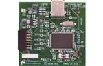
Thermocouple Sensor Board Version 1
SP1202S02RB
Users' Guide
© 2009 National Semiconductor Corporation.
1
http://www.national.com
�Table of Contents
1.0 Introduction............................................................................................................................ 3
2.0 Board Assembly .................................................................................................................... 3
3.0 Quick Start............................................................................................................................. 3
4.0 Functional Description........................................................................................................... 4
4.1 Operational Modes................................................................................................... 4
4.1.1 The Computer Mode ................................................................................ 4
4.1.2 The Stand-Alone Mode ............................................................................ 4
4.2 Signal Conditioning Circuitry .................................................................................... 4
4.2.1 Non-inverting Amplifier Configuration ...................................................... 4
4.2.2 Differential Amplifier Configuration .......................................................... 4
4.2.3 Level Shifting............................................................................................ 4
4.2.4 Offset and Gain Correction ...................................................................... 5
4.3 Cold Junction Reference Temperature Sensor ....................................................... 5
4.4 Power Supply ........................................................................................................... 5
4.5 Negative Bias Generation ........................................................................................ 5
4.6 ADC Reference Circuitry.......................................................................................... 5
4.7 ADC Serial Clock ..................................................................................................... 5
4.8 ADC Chip Select Bar................................................................................................ 5
4.9 Digital Data Output/Input.......................................................................................... 5
4.10 Power Requirements.............................................................................................. 5
5.0 Installing and Using the Thermocouple Sensor Board Version 1 ......................................... 5
5.1 Board Set-up ............................................................................................................ 5
5.2 Quick Check of Analog Functions............................................................................ 6
5.3 Quick Check of Software and Computer Interface Operation ................................. 6
5.4 Sensor Panel Software ............................................................................................ 6
5.5 Troubleshooting ....................................................................................................... 6
6.0 Evaluation Board Specifications............................................................................................ 6
7.0 Example Hardware Schematic.............................................................................................. 7
8.0 Thermocouple Sensor Board Version 1 Example Bill of Materials ....................................... 8
Summary Tables of Test Points and Connectors ....................................................................... 9
Summary Tables of Test Points and Connectors (cont'd) .......................................................... 10
Negative Bias Generation with LM2687 Circuit ........................................................................ 11
2
http://www.national.com
�1.0 Introduction
3.0 Quick Start
The Thermocouple Sensor Board Version 1
(SP1202S02RB) along with the Sensor Signal Path
Control Panel (Sensor Panel) software and SPUSI2
USB Interface Dongle are designed to ease the
design of circuits using various thermocouple
sensors with National's amplifiers and Analog-toDigital converters (ADCs). Use the WEBENCH®
Thermocouple Sensor Designer tool to determine
appropriate IC’s and passives to achieve your signal
path
requirements:
http://www.national.com/analog/webench/sensors/the
rmocouple
Refer to Figure 1 for locations of test points and
major components.
1. Place the jumpers on the following positions
See Figure 1 for component placement and Figure 2
for example board schematic. The thermocouple
sensor can be connected to header J1 or J2. The
differential voltage at the thermocouple sensor output
is digitized and can be captured and displayed on the
computer monitor with the accompanying Sensor
Panel software, which operates under Microsoft
Windows XP. The amplified thermocouple sensor
voltage may be measured at TP3 relative to ground.
The software can provide gain and offset correction
for the entire circuit, including the sensor.
2.0 Board Assembly
This Thermocouple Sensor Board Version 1 comes
as a bare board that must be assembled. Refer to an
example Bill of Materials for a description of
component values, to Figure 1 for major component
placement and to Figure 2 for the example Board
schematic.
TP4
ADC_IN1
TP2
-IN
Table 1 – NI Amplifier Jumper Positions
Pins
Jumper
FUNCTION
Shorted
JP1
2-3
NI/Diff Select
JP2
2-3
NI Level Shifting (a)
JP3
1-2
NI Level Shifting (b)
JP4
Open
Diff Level Shifting
JP5
2-3
Negative Bias Generator
JP6
2-3
ADC Reference Select
2. Connect the Thermocouple Sensor Board
Version 1 to a SPUSI2 (USB Interface Dongle)
via 14-pin header J3 and connect a USB cable
between the SPUSI2 board and a PC USB port.
Red LEDs D2 on the Thermocouples Sensor
Board Version 1 and D1 on the SPUSI2 board
should come on if the PC is on.
4. Connect the thermocouple sensor to connector
J1 or J2 of the board.
5. If not already installed, install the Sensor Panel
software on the PC. Run the software.
JP5
NEG BIAS
TP11
VREF
JP6
VREF_SEL
J2 Thermocouple
Connector
TP8
3.3V
TP6
SCLK
J1 Thermocouple
Connector
J3 ADC
Interface
JP3
NI_B
TP9
DIN
TP10
+5V
TP5
DOUT
JP2
NI_A LS
TP1
+IN
JP1 NI/DIFF
SELECT
JP4
NI_A LS
TP3
ADC_IN2
TP7
CSB
Figure 1. Component and Test Point Locations
3
http://www.national.com
�4.0 Functional Description
The Thermocouple Board Version 1 component and
test point locations are shown in Figure 1. The board
schematic is shown in Figure 2.
Amplifier A1A amplifies the output of the
thermocouple sensor. The gain of the non-inverting
amplifier is
Gain = 1 + RF1 / RG1.
4.1 Operational Modes
This board may be use in one of two modes: the
Computer Mode using the SPUSI2 USB Interface
Dongle or the Stand-Alone Mode without the use of
the SPUSI2 USB Interface Dongle and a PC.
4.1.1 The Computer Mode
The board is intended for use in the Computer Mode
with a SPUSI2 board. The Sensor Panel software
controls the measurements by communicating with
the ADC via the device’s SPI interface. Power to both
boards is provided via USB.
4.1.2 The Stand-Alone Mode
The Stand-Alone Mode does not use the SPUSI2
board to capture data and upload it to a PC. To use
the board this way, the user must provide +5V at pin
14 of header J3 as well as provide ADC clock, Chip
Select, and Data In signals to the ADC at pins 3, 1,
and 7 respectively, of J3. ADC data output is
available at pin 5 of J3. Test Points TP6, TP7, TP9
and TP5 may also be used to insert/read these
signals. The range of frequencies for the ADC clock
is 1 MHz to 4 MHz. The CS rate can be as low as
desired, but no faster than 17 times the ADC clock
rate.
A low pass filter is formed by RG2 and C1 which has
a cutoff frequency of
Cutoff Frequency = 1 / ( 2 * pi * RG2 * C1)
The WEBENCH Thermocouple Sensor Designer tool
will provide appropriate component values to achieve
your application gain and cutoff frequency
requirements.
4.2.2 Differential Amplifier Configuration
If moderate noise pickup is expected on the
thermocouple sensor line a differential amplifier
configuration will offer increased common mode
rejection (CMR). To set up the board in the
differential amplifier configuration without supplying
negative bias to the amplifier or level shifting the
thermocouple sensor voltage ensure the jumpers are
in the following position
Table 2 – Differential Amplifier Jumper Positions
Pins
Jumper
FUNCTION
Shorted
JP1
1-2
NI/Diff Select
JP2
Open
NI Level Shifting (a)
JP3
1-2
NI Level Shifting (b)
4.2 Signal Conditioning Circuitry
JP4
2-3
Diff Level Shifting
The sensor output voltage is amplified and digitized
by U4, an ADC. The full-scale value of this voltage
after amplification will depend upon the maximum
sensor output and the component values. This
amplified voltage is presented to the ADC (U4),
whose output is at header J3.
JP5
2-3
Negative Bias Generator
JP6
2–3
ADC Reference Select
4.2.1 Non-inverting (NI) Amplifier
Configuration
Amplifier A1A amplifies the differential output of the
thermocouple sensor. The gain of the differential
amplifier, assuming RG1 = RG2 and RF1 = RF2 is
Gain = RF1 / RG1
When minimal noise pickup is expected on the
thermocouple sensor line a non-inverting amplifier
configuration can be used. To set up the board in the
non-inverting
amplifier
configuration
without
supplying negative bias to the amplifier or level
shifting the thermocouple sensor voltage ensure the
jumpers are in the following position
Table 2 – NI Amplifier Jumper Positions
Pins
Jumper
FUNCTION
Shorted
A low pass filter is formed by CF1 = CF2, and RF1 =
RF2 which has a cutoff frequency of
Cutoff Frequency = 1 / ( 2 * pi * RF1 * CF1)
The Webench® Thermocouple Sensor Designer tool
will provide appropriate component values to achieve
your application gain and cutoff frequency requirements.
4.2.3 Level Shifting
JP1
2-3
NI/Diff Select
JP2
2-3
NI Level Shifting (a)
JP3
1-2
NI Level Shifting (b)
JP4
Open
Diff Level Shifting
JP5
2-3
Negative Bias Generator
JP6
2-3
ADC Reference Select
4
In many thermocouple applications the thermocouple
sensor is used in a temperature range where only a
positive output at the (+) terminal with respect to the
(-) terminal or only a negative output is expected. If
both positive and negative voltage is expected the
board allows for an offset which is provided from a
level shifting circuit. The level shifting voltage is set
up by VREF and the RLS1-RLS2 voltage divider,
then buffered through amplifier A1B. The level
shifting voltage is
http://www.national.com
�VLS = (VREF * RLS2) / (RLS2 + RLS1)
The Webench® Thermocouple Sensor Designer tool
will provide appropriate component values to achieve
your application level shifting requirements.
To add level shifting to the differential amplifier
configuration change the following jumper
Table 4 – Diff Amp Level Shifting Jumper Positions
Jumper
Pins
Shorted
FUNCTION
JP4
1-2
Diff Level Shifting
To add level shifting to the non-inverting amplifier
configuration change the following jumper
Table 5 – NI Amp Level Shifting Jumper Positions
Jumper
Pins
Shorted
FUNCTION
JP2
1-2
NI Level Shifting (a)
In the case where the measured temperature is close
to the ambient cold junction reference temperature
and the output voltage of the amplifying amplifier A1A
is very low it is possible that the amplifier output may
saturate. To avoid amplifier output saturation the
board allows for a negative bias to be applied to the
V- terminal of the amplifier. An external negative bias
source can be connected to the V- terminal of the
amplifier at pin 2 of JP5. Pin 3 of JP5 which is ground
can be used as a reference. Alternatively see the
Appendix to see how you can use the unpopulated
LM2687 circuit as a negative bias generator.
4.6 ADC Reference Circuitry
The single-ended dual channel ADCXX2SXX1 uses its
supply voltage as its reference, so it is important that
its supply voltage be stable and quiet. A 4.1V
reference voltage is provided by U3, an accurate
LM4120-4.1.
4.7 ADC Serial Clock
4.2.4 Offset and Gain Correction
The circuitry does not provide adjustment for offset
voltages. However, the Sensor Panel software does
allow for this correction.
4.3 Cold Junction Reference Temperature
Sensor
A thermocouple sensor has the ability to measure a
temperature differential between the measured
temperature point and the reference temperature
point at the reference junction often referred to as the
cold junction. Due to this fact in order to determine
the correct absolute temperature at the measuring
point it is necessary to know the cold junction
reference temperature. This is accomplished on
board by the LM94022 Analog Temperature Sensor,
U2, who’s output is fed to the first channel of the
ADC, U4. The Sensor Panel software takes this data
then calculates the correct absolute temperature at
the measuring point. The LM94022 mV/C transfer
function can be found in the LM94022 datasheet. The
sensor is hard wired for gain setting GS = 11.
4.4 Power Supply
In Computer Mode, power to this board is supplied
through header J3 and ultimately from the host PC
via USB. In most cases, the only voltage needed for
the Thermocouple Sensor Board Version 1 is the +5V
from the USB connection. Diode D1 provides
protection against reverse polarity in the Stand-Alone
mode where an external supply is used.
The supply voltage source for the ADC (VREF on the
schematic) is selected with JP6 to be either the 4.1V
from U3, or +5V from J3.
4.5 Negative Bias Generation
5
The ADC clock signal (SCLK) is provided external to the
board at header J3 on pin 3 or TP6. The requirements
for SCLK can be found in the respective ADC datasheet.
4.8 ADC Chip Select Bar
The ADC chip select bar (CSB) is provided external
to the board at header J3 on pin 1 or on TP7. The
requirements for CSB with respect to SCLK can be
found in the respective ADC datasheet.
4.9 Digital Data Output/Input
The digital output data from the ADC is available at
14-pin header J3 on pin 5 or on TP5. The digital input
data to the ADC is available at 14-pin header J3 on
pin 7 or on TP9.
4.10 Power Requirements
Voltage and current requirements for
Thermocouple Sensor Board Version 1 are:
the
Pin 14 of J3: +5.0V at 30 mA
Pins 2 and 4 of J3: Ground
5.0 Installing and Using the Thermocouple
Sensor Board Version 1
The Thermocouple Sensor Board Version 1 requires
power as described above. The thermocouple sensor
should be connected to J1 or J2.
5.1 Board Set-up
Refer to Figure 1 for locations of connectors, test
points and jumpers on the board.
1. Connect The Thermocouple Sensor Board
Version 1 to a SPUSI2 USB Interface Dongle.
2. Be sure all jumpers are in place per Table 2 for
Differential Amplifier or Table 3 for Non-inverting
Amplifier.
3. Connect the thermocouple sensor to J1 or J2.
http://www.national.com
�4. Connect a USB cable to the SPUSI2 board and a
PC.
5. Confirm that Red LED D2 on the Thermocouple
Sensor Board Version 1 is on, indicating the
presence of power to the board.
5.2 Quick Check of Analog Functions
Refer to Figure 1 for locations of connectors and test
points and jumpers on the board. If at any time the
expected response is not obtained, see Section 5.5
on Troubleshooting.
1. Perform steps 1 through 4 of Section 5.1.
2. Check for 5.0V at TP10 and for 4.1V at TP11.
3. Apply a known voltage, Vin, at J1 or J2 connector
and based on chosen gain, Av, of circuit confirm
that voltage, Vout, at TP3 is as expected (Vin x
Av = Vout).
4. Check temperature sensor output voltage at TP4
is as expected according to the transfer table
found in the LM94022 datasheet. Room temp is
apx. 2.3V.
5. Check negative bias generator output voltage at
pin 1 of JP5 is apx. -0.25V.
6. Check level shifting output voltage at pin 1 of JP2
is VLS = (VREF * RLS2) / (RLS2 + RLS1)
This completes the quick check of the analog portion
of the evaluation board.
5.5 Troubleshooting
If there is no output from the board, check the
following:
Be sure that the proper voltages and polarities
are present at TP10 (+5V) and TP11 (+4.1V or
+5V, as selected with JP6).
Be sure there is a clock signal at TP6 when trying
to capture data.
Confirm thermocouple sensor is connected
properly.
If the ADC output is zero or a single code, check the
following:
Be sure that the proper voltages and polarities
are present at TP10 (+5V) and TP11 (+4.1V or
+5V, as selected with JP6).
Be sure that J3 is properly connected to a
SPUSI2 USB Interface Dongle, and that there is
a jumper on JP6.
Confirm thermocouple
properly.
sensor is connected
6.0 Evaluation Board Specifications
5.3 Quick Check of Software and Computer
Interface Operation
1.
2.
3.
4.
Perform steps 1 through 4 of Section 5.1.
Run the Sensor Panel software.
Select the SPI202S02RB
Manually enter the following data:
Thermocouple Type
Amplifier Configuration (Always select
“Instr/Diff”)
Gain
Level Shifting Voltage
Number of bits
ADC Reference Voltage
The software will display the cold junction reference
temperature and the thermocouple measured
temperature.
This completes the quick check of the software and
computer interface.
Board Size:
2.85" x 2.30" (7.2 cm x 5.8 cm)
Power Requirements: +5V (30mA) at J3 pin 14
5.4 Sensor Panel Software
The Sensor Panel software is available on the web at
http:\\www.national.com
Upon loading the software and running it, it is
necessary to configure it for the board you are using.
See the Sensor Panel software User’s Guide for
more details.
6
http://www.national.com
�7.0 Example Hardware Schematic
Figure 2. Thermocouple Sensor Board Version 1 Schematic
7
http://www.national.com
�8.0 Thermocouple Sensor Board Version 1 Example Bill of Materials
Item
#
Quantity
1
6
Reference
C4, C6, C8, C9, C11,
C14
2
1
C2
Capacitor, Ceramic, 0.001uF, SMT, 0603, X7R, 50V,
10%
3
3
C3, C7, C10
Capacitor, Tantalum, 10uF, SMT, 3528, 10V, 10%
4
1
C5
Capacitor, Tantalum, 4.7uF, SMT, 3528, 10V, 10%
5
1
C1
Selected by WEBENCH® Sensor Designer
6
1
CS
Selected by WEBENCH® Sensor Designer
7
2
CF1, CF2
Selected by WEBENCH® Sensor Designer
8
1
C12
NOT STUFFED
9
1
C13
Capacitor, Ceramic, 0.033uF, SMT, 0603, X7R, 50V,
10%
10
4
CN1, CN2, CN3, CN4
Capacitor, Ceramic, 1uF, SMT, 1206, 16V, 10%
11
1
D1
DIODE, 50V, 1A
12
1
D2
RED LED
13
1
J1
Terminal Block
14
1
J2
Thermocouple Connector
15
1
J3
ADC INTERFACE
16
6
JP1 - JP6
3-PIN HEADER
17
1
R1
Resistor, SMT, 0603, 1%, 43.0 ohm
18
2
RLS1, RLS2
Selected by WEBENCH® Sensor Designer
19
1
RN1
See Appendix - Negative Bias Generation with LM2687
Circuit
20
1
RN2
See Appendix - Negative Bias Generation with LM2687
Circuit
21
2
RF1, RF2
Selected by WEBENCH® Sensor Designer
22
1
RN4
Resistor, SMT, 0603, 1%, 100ohm
23
1
RN3
NOT STUFFED
24
1
RS
Selected by WEBENCH® Sensor Designer
25
1
R2,
Resistor, SMT, 0603, 1%, 1.00Kohm
RG1, RG2
Selected by WEBENCH® Sensor Designer
26
2
13
TP1-TP10, TPG1TPG3
TEST POINTS (NOT STUFFED)
1
U1
LM2687
1
U2
LM94022
1
U3
LM4120AIM5-4.1
1
U4
Selected by WEBENCH® Sensor Designer
1
VR1
NOT STUFFED. Short pins 1 & 2.
1
A1
Selected by WEBENCH® Sensor Designer
Part
Reference
Capacitor, Ceramic, 0.1uF, SMT, 0603, X7R, 25V, 10%
TDK # C1608X7R1E104K
Digi-key # 445-1316-1-ND
KEMET # C0603C102K5RACTU
Digi-key # 399-1082-1-ND
VISHAY # 293D106X9010B2TE3
Digi-key # 718-1122-1-ND
VISHAY # 293D475X9010B2TE3
Digi-Key # 718-1147-1-ND
MURATA #
GRM188R71H333KA61D
Digi-key # 490-3286-1-ND
JOHANSON # 160R18W105KV4E
Digi-key # 709-1068-1-ND
MCC # GS1A-TP
Digi-key # GS1A-TPCT-ND
LITE-ON # LTST-C930KAKT
Digi-key # 160-1461-1-ND
ON SHORE # ED120/2DS
Digi-key # ED1609-ND
OMEGA #PCC-SMP
TYCO # 87230-7
Digi-key # A26599-ND
Waldom/Molex # 22-28-4033
Digi-key # WM6503-ND
Panasonic # ERJ-3EKF43R0V
Digi-key # P43.0HCT-ND
Panasonic #ERJ-3EKF1000V
Digi-key # P100HCT-ND
Panasonic # ERJ-3EKF1001V
Digi-key # P1.00KHCT-ND
27
NSC # LM2687MM/NOPB
Digi-key # LM2687MMCT-ND
NSC # LM94022QBIMG/NOPB
Digi-key # LM94022QBIMGCT-ND
NSC # LM4120AIM5-4.1/NOPB
Digi-key # LM4120AIM5-4.1CT-ND
28
29
30
31
32
33
8
http://www.national.com
�APPENDIX
Summary Tables of Test Points and Connectors
Test Points on the Thermocouple Sensor Board Version 1
Identifier
TP 1
TP 2
TP 3
TP 4
TP 5
TP 6
TP 7
TP 8
TP 9
TP 10
TP 11
Name
+IN
-IN
ADC_IN2
ADC_IN1
DOUT
SCLK
CSb
+3V3
DIN
+5V
VREF
Function
+IN of A1A amplifier
-IN of A1A amplifier
ADC Channel 2 input voltage
ADC Channel 1 input voltage
DOUT output from ADC
SCLK input for ADC
CSb input for ADC
+3.3V from SPUSI2 Board (not used on this board)
DIN input for ADC
Overall supply for board from SPUSI2 Board
Supply/Reference voltage of ADC
J1/J2 Connector - Sensor Interface
Identifier
J1/J2-1
J1/J2-2
Name
-Out
+Out
Function
- Output from Sensor
+ Output from Sensor
J3 Connector - Connection to SPUSI2 Board
J3 Pin Number
1
2
3
4
5
6
7
8
9
10
11
12
13
14
Voltage or Signal
CSb input to ADC
Ground
SCLK input to ADC
Ground
SDATA output from ADC
no connection
DIN input to ADC
no connection
no connection
no connection
no connection
no connection
+3.3V from SPUSI2 USB Interface Dongle
+5V from SPUSI2 USB Interface Dongle
9
http://www.national.com
�Summary Tables of Test Points and Connectors (cont'd)
JP1 Jumper – NI/Diff Select
Shorted Positions
1-2
2-3
Results
Non-inverting amplifier configuration
Differential amplifier configuration
JP2 Jumper – NI Level Shifting (a)
Shorted Positions
1-2
2-3
Results
Non-inverting amplifier level shifting enabled
Non-inverting amplifier level shifting disabled
JP3 Jumper – NI Level Shifting (b)
Shorted Positions
1-2
2-3
Results
Default
Not used
JP4 Jumper – Diff Level Shifting
Shorted Positions
1-2
2-3
Results
Differential amplifier level shifting enabled
Differential amplifier level shifting disabled
JP5 Jumper – Negative Bias Generator
Shorted Positions
Open
1-2
2-3
Results
Negative bias generation enabled – Connect external supply to pin 2
Negative bias generation enabled – LM2687 Circuit
Negative bias generation disabled
JP6 Jumper – ADC Reference Select
Shorted Positions
1-2
2-3
Results
+5V for ADC supply and reference voltage
+4.1V for ADC supply and reference voltage
10
http://www.national.com
�Negative Bias Generation with LM2687 Circuit
To avoid amplifier output saturation the board allows for a negative bias from the unpopulated LM2687 circuit to
be applied to the V- terminal of the amplifier. The regulated output for the LM2687 voltage inverter, U1, is
adjustable between −1.5V and −5.2V. When selecting a negative voltage for the V- terminal of the amplifier be
aware not to exceed the max supply voltage operating ratings for the amplifier selected. The output voltage can
be selected using the equation
Vout = ( RN2 / RN1 ) * (VFB – VADJ) + VFB
Where the feedback pin is held at a constant voltage VFB which equals −1.2V and on this board VADJ will be
shorted to ground. This simplifies the equation to
Vout = ( RN2 / RN1 ) * (-1.2V) – 1.2V
For example to set Vout = -1.5V one could select RN2 = 20 kΩ and RN1 = 78.7 kΩ.
To set up the circuit on board do not populate RN3 or VR1. Short pad 1 to pad 2 of VR1. To connect output of
LM2687 circuit to V- terminal of the amplifier short pins 1 and 2 of jumper 5 (JP5).
11
http://www.national.com
�The Thermocouple Sensor Board Version 1 is intended for product evaluation purposes only and is not intended for resale to end
consumers, is not authorized for such use and is not designed for compliance with European EMC Directive 89/336/EEC.
National does not assume any responsibility for use of any circuitry or software supplied or described. No circuit patent licenses are implied.
LIFE SUPPORT POLICY
NATIONAL'S PRODUCTS ARE NOT AUTHORIZED FOR USE AS CRITICAL COMPONENTS IN LIFE SUPPORT DEVICES OR SYSTEMS
WITHOUT THE EXPRESS WRITTEN APPROVAL OF THE PRESIDENT OF NATIONAL SEMICONDUCTOR CORPORATION. As used
herein:
1. Life support devices or systems are devices or systems
which, (a) are intended for surgical implant into the body, or
(b) support or sustain life, and whose failure to perform,
when properly used in accordance with instructions for use
provided in the labeling, can be reasonably expected to
result in a significant injury to the user.
National Semiconductor Corporation
Americas
Tel:
1-800-272-9959
Fax: 1-800-737-7018
Email: support@nsc.com
National Semiconductor Europe
Fax: +49 (0) 1 80-530 85 86
Email: europe.support@nsc.com
Deutsch Tel: +49 (0) 1 80-530 85 85
English Tel: +49 (0) 1 80 532 78 32
Français Tel: +49 (0) 1 80 532 93 58
Italiano Tel: +49 (0) 1 80 534 16 8
2. A critical component is any component in a life support
device or system whose failure to perform can be reasonably
expected to cause the failure of the life support device or
system, or to affect its safety or effectiveness.
National Semiconductor
Asia Pacific Customer
Response Group
Tel: 65-2544466
Fax: 65-2504466
Email: sea.support@nsc.com
National Semiconductor
Japan Ltd.
Tel: 81-3-5620-6175
Fax: 81-3-5620-6179
www.national.com
National does not assume any responsibility for any circuitry described, no circuit patent licenses are implied and National reserves the right at any time without
notice to change said circuitry and specifications.
12
http://www.national.com
�IMPORTANT NOTICE
Texas Instruments Incorporated and its subsidiaries (TI) reserve the right to make corrections, modifications, enhancements, improvements,
and other changes to its products and services at any time and to discontinue any product or service without notice. Customers should
obtain the latest relevant information before placing orders and should verify that such information is current and complete. All products are
sold subject to TI’s terms and conditions of sale supplied at the time of order acknowledgment.
TI warrants performance of its hardware products to the specifications applicable at the time of sale in accordance with TI’s standard
warranty. Testing and other quality control techniques are used to the extent TI deems necessary to support this warranty. Except where
mandated by government requirements, testing of all parameters of each product is not necessarily performed.
TI assumes no liability for applications assistance or customer product design. Customers are responsible for their products and
applications using TI components. To minimize the risks associated with customer products and applications, customers should provide
adequate design and operating safeguards.
TI does not warrant or represent that any license, either express or implied, is granted under any TI patent right, copyright, mask work right,
or other TI intellectual property right relating to any combination, machine, or process in which TI products or services are used. Information
published by TI regarding third-party products or services does not constitute a license from TI to use such products or services or a
warranty or endorsement thereof. Use of such information may require a license from a third party under the patents or other intellectual
property of the third party, or a license from TI under the patents or other intellectual property of TI.
Reproduction of TI information in TI data books or data sheets is permissible only if reproduction is without alteration and is accompanied
by all associated warranties, conditions, limitations, and notices. Reproduction of this information with alteration is an unfair and deceptive
business practice. TI is not responsible or liable for such altered documentation. Information of third parties may be subject to additional
restrictions.
Resale of TI products or services with statements different from or beyond the parameters stated by TI for that product or service voids all
express and any implied warranties for the associated TI product or service and is an unfair and deceptive business practice. TI is not
responsible or liable for any such statements.
TI products are not authorized for use in safety-critical applications (such as life support) where a failure of the TI product would reasonably
be expected to cause severe personal injury or death, unless officers of the parties have executed an agreement specifically governing
such use. Buyers represent that they have all necessary expertise in the safety and regulatory ramifications of their applications, and
acknowledge and agree that they are solely responsible for all legal, regulatory and safety-related requirements concerning their products
and any use of TI products in such safety-critical applications, notwithstanding any applications-related information or support that may be
provided by TI. Further, Buyers must fully indemnify TI and its representatives against any damages arising out of the use of TI products in
such safety-critical applications.
TI products are neither designed nor intended for use in military/aerospace applications or environments unless the TI products are
specifically designated by TI as military-grade or "enhanced plastic." Only products designated by TI as military-grade meet military
specifications. Buyers acknowledge and agree that any such use of TI products which TI has not designated as military-grade is solely at
the Buyer's risk, and that they are solely responsible for compliance with all legal and regulatory requirements in connection with such use.
TI products are neither designed nor intended for use in automotive applications or environments unless the specific TI products are
designated by TI as compliant with ISO/TS 16949 requirements. Buyers acknowledge and agree that, if they use any non-designated
products in automotive applications, TI will not be responsible for any failure to meet such requirements.
Following are URLs where you can obtain information on other Texas Instruments products and application solutions:
Products
Applications
Audio
www.ti.com/audio
Automotive and Transportation www.ti.com/automotive
Amplifiers
amplifier.ti.com
Communications and Telecom www.ti.com/communications
Data Converters
dataconverter.ti.com
Computers and Peripherals
www.ti.com/computers
DLP® Products
www.dlp.com
Consumer Electronics
www.ti.com/consumer-apps
DSP
dsp.ti.com
Energy and Lighting
www.ti.com/energy
Clocks and Timers
www.ti.com/clocks
Industrial
www.ti.com/industrial
Interface
interface.ti.com
Medical
www.ti.com/medical
Logic
logic.ti.com
Security
www.ti.com/security
Power Mgmt
power.ti.com
Space, Avionics and Defense
www.ti.com/space-avionics-defense
Microcontrollers
microcontroller.ti.com
Video and Imaging
www.ti.com/video
RFID
www.ti-rfid.com
OMAP Mobile Processors
www.ti.com/omap
Wireless Connectivity
www.ti.com/wirelessconnectivity
TI E2E Community Home Page
e2e.ti.com
Mailing Address: Texas Instruments, Post Office Box 655303, Dallas, Texas 75265
Copyright © 2012, Texas Instruments Incorporated
�