Sample &
Buy
Product
Folder
Support &
Community
Tools &
Software
Technical
Documents
TAS5720L, TAS5720M
SLOS903B – MAY 2015 – REVISED FEBRUARY 2016
TAS5720x Digital Input Mono Class-D Audio Amplifier
With TDM Support Up To 8 Channels
1 Features
3 Description
•
The TAS5720x device is a high-efficiency mono
Class-D audio power amplifier optimized for high
transient power capability to use the dynamic power
headroom of small loudspeakers. The device is
capable of delivering more than 15 W continuously
into a 4-Ω speaker.
1
•
•
•
•
•
Mono Class-D Amplifier
– 20 W at 0.15% THD Continuous into
19 V / 4 Ω
TDM Audio Input
– Up to 8 Channels (32-bit, 48 kHz)
I2C Control With 8 Selectable I2C Address
Power Supplies
– Power Amplifier: 4.5 V to 16.5 V, TAS5720L
– Power Amplifier: 4.5 V to 26.4 V, TAS5720M
– Digital I/O: 3.3 V
Protection: Thermal and Short-Circuit
Package: 4 mm × 4 mm, 32-pin VQFN
The digital time division multiplexed (TDM) interface
enables up to eight devices to share the same bus.
The TAS5720x device is available in a 32-pin,
4 mm × 4 mm, VQFN package for a compact PCB
footprint.
Device Information(1)
PART NUMBER
TAS5720L
2 Applications
•
•
•
•
VQFN (32)
TAS5720M
Sub Woofers
Boom Boxes
Bar Speakers
Surround Sound Systems
PACKAGE
BODY SIZE (NOM)
4.00 mm × 4.00 mm
(1) For all available packages, see the orderable addendum at
the end of the datasheet.
Simplified Schematic
PVDD
DVDD
SDZ
x
x
x
ADR0
ADR1
BST_P
Protections:
Pop/Click
Overcurrent
Over Temperature
OUT_P
ClosedLoop
Class-D
Amplifier
SCL
SDA
FAULTZ
System
Interface
AVDD
4.5 V - 16.5 V, TAS5720L
4.5 V - 26.4 V, TAS5720M
3.3 V
OUT_N
DAC
BST_N
SDIN
LRCLK
PGND
GVDD
VCOM
VREF_N
TAS5720L/M
GND
MCLK
VREG
Voltage
Regulators
BCLK
1
An IMPORTANT NOTICE at the end of this data sheet addresses availability, warranty, changes, use in safety-critical applications,
intellectual property matters and other important disclaimers. PRODUCTION DATA.
�TAS5720L, TAS5720M
SLOS903B – MAY 2015 – REVISED FEBRUARY 2016
www.ti.com
Table of Contents
1
2
3
4
5
6
Features ..................................................................
Applications ...........................................................
Description .............................................................
Revision History.....................................................
Pin Configuration and Functions .........................
Specifications.........................................................
6.1
6.2
6.3
6.4
6.5
6.6
6.7
7
1
1
1
2
3
5
Absolute Maximum Ratings ...................................... 5
ESD Ratings.............................................................. 5
Recommended Operating Conditions....................... 5
Thermal Information .................................................. 5
Electrical Characteristics........................................... 6
Timing Requirements ................................................ 9
Typical Characteristics ............................................ 12
Detailed Description ............................................ 19
7.1 Overview ................................................................. 19
7.2 Functional Block Diagram ....................................... 19
7.3 Feature Description................................................. 19
7.4 Device Functional Modes ....................................... 30
7.5 Register Maps ......................................................... 32
8
Applications and Implementation ...................... 40
8.1 Application Information............................................ 40
8.2 Typical Application .................................................. 40
9 Power Supply Recommendations...................... 42
10 Layout................................................................... 42
10.1 Layout Guidelines ................................................. 42
10.2 Layout Example .................................................... 43
11 Device and Documentation Support ................. 44
11.1
11.2
11.3
11.4
11.5
Documentation Support ........................................
Community Resources..........................................
Trademarks ...........................................................
Electrostatic Discharge Caution ............................
Glossary ................................................................
44
44
44
44
44
12 Mechanical, Packaging, and Orderable
Information ........................................................... 44
4 Revision History
NOTE: Page numbers for previous revisions may differ from page numbers in the current version.
Changes from Revision A (November 2015) to Revision B
Page
•
Updated Typical Characteristics graphs with new data, new standards. ............................................................................. 12
•
Added new Layout Example ................................................................................................................................................ 43
Changes from Original (September 2015) to Revision A
•
2
Page
Production release ................................................................................................................................................................. 1
Submit Documentation Feedback
Copyright © 2015–2016, Texas Instruments Incorporated
Product Folder Links: TAS5720L TAS5720M
�TAS5720L, TAS5720M
www.ti.com
SLOS903B – MAY 2015 – REVISED FEBRUARY 2016
5 Pin Configuration and Functions
GVDD
GND
AVDD
PVDD
PVDD
OUT_P
29
28
27
26
25
31
30
VCOM
VREG
32
RSM Package
VQFN 32 PINS
Top View
VREF_N
1
24
OUT_P
FAULTZ
2
23
BST_P
SDZ
3
22
PGND
LRCLK
4
21
PGND
MCLK
5
20
PGND
BCLK
6
19
PGND
SDIN
7
18
BST_N
SCL
8
17
OUT_N
16
OUT_N
PVDD
14
15
PVDD
13
ADR0
11
12
ADR1
GND
DVDD
9
SDA
10
Exposed Thermal Pad
Pin Functions
PIN
I/O/P (1)
DESCRIPTION
NAME
NO.
ADR1
12
I
ADR0
13
I
I2C address inputs. Each pin can detect a short to DVDD, a short to GND, a 22-kΩ connection to GND,
and a 22-kΩ connection to DVDD.
AVDD
28
P
Analog power supply input. Connect directly to PVDD.
BST_N
18
P
Class-D Amplifier negative bootstrap. Connect to a capacitor between BST_N and OUT_N.
BST_P
23
P
Class-D Amplifier positive bootstrap. Connect to a capacitor between BST_P and OUT_P.
DVDD
11
P
Digital power supply. Connect to a 3.3-V supply with external decoupling capacitor.
FAULTZ
2
O
Open drain active low fault flag. Pull up on PCB with resistor to DVDD.
LRCLK
4
I
TDM interface frame synchronization.
P
Ground. Connect to PCB ground plane.
GND
10
29
GVDD
30
O
Class-D amplifier gate drive regulator output. Connect decoupling cap to PCB ground plane.
MCLK
5
I
Device master clock.
P
Power ground. Connect to PCB ground plane.
P
Class-D amplifier power supply input. Connect to PVDD supply and decouple externally.
O
Class-D amplifier negative output.
O
Class-D amplifier positive output.
I
TDM Interface serial bit clock.
19
PGND
20
21
22
14
PVDD
15
26
27
OUT_N
OUT_P
BCLK
(1)
16
17
24
25
6
I = input, O = output, P = power, I/O = bi-directional
Copyright © 2015–2016, Texas Instruments Incorporated
Product Folder Links: TAS5720L TAS5720M
Submit Documentation Feedback
3
�TAS5720L, TAS5720M
SLOS903B – MAY 2015 – REVISED FEBRUARY 2016
www.ti.com
Pin Functions (continued)
PIN
NAME
NO.
I/O/P (1)
DESCRIPTION
I2C clock Input. Pull up on PCB with a 2.4-kΩ resistor.
SCL
8
I
SDA
9
I/O
SDIN
7
I
TDM interface data input.
SDZ
3
I
Active low shutdown signal. Assert low to hold device inactive.
Thermal
Pad
33
G
Connect to GND for best system performance. If not connected to GND, leave floating.
VCOM
32
O
Common mode reference output. Connect decoupling capacitor to the VREF_N pin.
VREF_N
1
P
Negative reference for analog. Connect to VCOM and VREG capacitor negative pins.
VREG
31
O
Analog regulator output. Connect decoupling capacitor to the VREF_N pin.
4
I2C bi-directional data. Pull up on PCB with a 2.4-kΩ resistor.
Submit Documentation Feedback
Copyright © 2015–2016, Texas Instruments Incorporated
Product Folder Links: TAS5720L TAS5720M
�TAS5720L, TAS5720M
www.ti.com
SLOS903B – MAY 2015 – REVISED FEBRUARY 2016
6 Specifications
6.1 Absolute Maximum Ratings
over operating free-air temperature range (unless otherwise noted) (1)
Supply voltage (2)
Digital input voltage
MIN
MAX
PVDD, AVDD (TAS5720L)
–0.3
20
UNIT
PVDD, AVDD (TAS5720M)
–0.3
30
DVDD
–0.3
4
Digital inputs referenced to DVDD supply
–0.5
VDVDD + 0.5
V
V
Ambient operating temperature, TA
–25
85
°C
Storage temperature, Tstg
–40
125
°C
(1)
(2)
Stresses beyond those listed under Absolute Maximum Ratings can cause permanent damage to the device. These are stress ratings
only, and functional operation of the device at these or any other conditions beyond those indicated under Recommended Operating
Conditions is not implied. Exposure to absolute-maximum-rated conditions for extended periods can affect device reliability.
All voltages are with respect to network ground pin.
6.2 ESD Ratings
VALUE
V(ESD)
(1)
(2)
Electrostatic
discharge
Human body model (HBM), per ANSI/ESDA/JEDEC JS-001, (1)
±4000
Charged device model (CDM), per JEDEC specification JESD22-C101 (2)
±1500
UNIT
V
JEDEC document JEP155 states that 500-V HBM allows safe manufacturing with a standard ESD control process.
JEDEC document JEP157 states that 250-V CDM allows safe manufacturing with a standard ESD control process.
6.3 Recommended Operating Conditions
over operating free-air temperature range (unless otherwise noted)
MAX
UNIT
TAS5720L
MIN
4.5
TYP
16.5
V
TAS5720M
4.5
26.4
V
3.6
V
PVDD/
AVDD
Power supply voltage
DVDD
Power supply voltage
VIH(DR)
High-level digital input voltage
VDVDD
VIL(DR)
Low-level digital input voltage
0
RSPK
Minimum speaker load
3.2
TA
Operating free-air temperature
–25
85
°C
TJ
Operating junction temperature
–25
150
°C
3
3.3
V
V
Ω
6.4 Thermal Information
TAS5720x
THERMAL METRIC (1)
RSM (VQFN)
UNIT
32 PINS
RθJA
Junction-to-ambient thermal resistance
37.3
°C/W
RθJCtop
Junction-to-case (top) thermal resistance
30.4
°C/W
RθJB
Junction-to-board thermal resistance
7.9
°C/W
ψJT
Junction-to-top characterization parameter
0.4
°C/W
ψJB
Junction-to-board characterization parameter
7.7
°C/W
RθJCbot
Junction-to-case (bottom) thermal resistance
2.5
°C/W
(1)
For more information about traditional and new thermal metrics, see the Semiconductor and IC Package Thermal Metrics application
report (SPRA953).
Copyright © 2015–2016, Texas Instruments Incorporated
Product Folder Links: TAS5720L TAS5720M
Submit Documentation Feedback
5
�TAS5720L, TAS5720M
SLOS903B – MAY 2015 – REVISED FEBRUARY 2016
www.ti.com
6.5 Electrical Characteristics
TA = 25ºC, V(PVDD) = 15 V, V(DVDD) = 3.3 V, RL = 4 Ω, fIN = 1 kHz, fs = 48 kHz, f(PWM) = 768 kHz, Gain = 20.7 dBV, SDZ = 1,
Measured with an Audio Precision SYS-2722 High-Performance Audio Analyzer and using a 15-µH, 0.68-µF reconstruction
filter at the device output.
PARAMETER
CONDITIONS
MIN
TYP
MAX
UNIT
DIGITAL INPUT AND OUTPUT
VIH
High-level digital input logic
voltage threshold
All digital pins
VIL
Low-level digital input logic
voltage threshold
All digital pins
IIH
Input logic "high" leakage for
digital inputs
All digital pins, excluding SDZ
15
µA
IIL
Input logic "low" leakage for
digital inputs
All digital pins, excluding SDZ
–15
µA
IIH(SDZ)
Input logic "high" leakage for
SDZ inputs
SDZ
1
µA
IIL(SDZ)
Input logic "low" leakage for
SDZ inputs
SDZ
–1
µA
VOL
Output logic "low" for FAULTZ
open drain Output
IOL = –2 mA
CIN
Input capacitance for digital
inputs
All digital pins
70% VDVDD
30% VDVDD
10% VDVDD
5
pF
MASTER CLOCK
D(MCLK)
Allowable MCLK duty cycle
45%
50%
MCLK input frequency
f(MCLK)
55%
25
Supported single-speed MCLK
frequencies
Values: 64, 128, 256, and 512
64 × fS
512 × fS
Supported double-speed MCLK
frequencies
Values: 64, 128, and 256
64 × fS
256 × fS
MHz
SERIAL AUDIO PORT
D(BCLK)
Allowable BCLK duty cycle
45%
50%
BCLK input frequency
f(BCLK)
fS
55%
25
MHz
Supported single-speed BCLK
frequencies
Values: 64, 128, 256, and 512
64 × fS
512 × fS
Supported double-speed BCLK
frequencies
Values: 64, 128, and 256
64 × fS
256 × fS
Supported single-speed input
sample rates
Values: 44.1 and 48
44.1
48
kHz
Supported double-speed input
sample rates
Values: 88.2 and 96
88.2
96
kHz
400
pF
400
kHz
2
I C CONTROL PORT
CL(I2C)
Allowable load capacitance for
each I2C Line
fSCL
SCL frequency
No wait states
PROTECTION
OTE(THRESH)
Overtemperature error (OTE)
threshold
150
°C
OTE(HYST)
Overtemperature error (OTE)
hysteresis
15
°C
OCE(THRESH)
Overcurrent error (OCE)
threshold
V(PVDD) = 16.5 V, TA = 25°C
6
A
DCE(THRESH)
DC error (DCE) threshold
V(PVDD) = 16.5 V, TA = 25°C
2.6
V
6
Submit Documentation Feedback
Copyright © 2015–2016, Texas Instruments Incorporated
Product Folder Links: TAS5720L TAS5720M
�TAS5720L, TAS5720M
www.ti.com
SLOS903B – MAY 2015 – REVISED FEBRUARY 2016
Electrical Characteristics (continued)
TA = 25ºC, V(PVDD) = 15 V, V(DVDD) = 3.3 V, RL = 4 Ω, fIN = 1 kHz, fs = 48 kHz, f(PWM) = 768 kHz, Gain = 20.7 dBV, SDZ = 1,
Measured with an Audio Precision SYS-2722 High-Performance Audio Analyzer and using a 15-µH, 0.68-µF reconstruction
filter at the device output.
PARAMETER
CONDITIONS
MIN
TYP
MAX
UNIT
AMPLIFIER PERFORMANCE
POUT
Continuous average power
RL= 4 Ω, 10% THD+N, V(PVDD) = 7.2 V,
fIN = 1 kHz
6.6
RL= 8 Ω, 10% THD+N, V(PVDD) = 7.2 V,
fIN = 1 kHz
3.7
RL= 4 Ω, 10% THD+N, V(PVDD) = 12 V,
fIN = 1 kHz
17.8
RL= 8 Ω, 10% THD+N, V(PVDD) = 12 V,
fIN = 1 kHz
10.1
RL= 4 Ω, 10% THD+N, V(PVDD) = 15 V,
fIN = 1 kHz, TA= 60°C
27.4
RL= 8 Ω, 10% THD+N, V(PVDD) = 15 V,
fIN = 1 kHz
15.8
RL= 4 Ω, 10% THD+N, V(PVDD) = 19 V,
fIN = 1 kHz
27
RL= 8 Ω, 10% THD+N, V(PVDD) = 19 V,
fIN = 1 kHz
25.3
RL= 4 Ω, 10% THD+N, V(PVDD) = 24 V,
fIN = 1 kHz
22.1
RL= 8 Ω, 10% THD+N, V(PVDD) = 24 V,
fIN = 1 kHz
THD+N
Total harmonic distortion plus
noise
W
39.8
RL= 4 Ω,V(PVDD) = 7.2 V, POUT = 1 W,
fIN = 1 kHz
0.033%
RL= 8 Ω,V(PVDD) = 7.2 V, POUT = 1 W,
fIN = 1 kHz
0.015%
RL= 4 Ω, V(PVDD)= 12 V, POUT = 1 W,
fIN = 1 kHz
0.03%
RL= 8 Ω, V(PVDD)= 12 V, POUT = 1 W,
20 Hz ≤ fIN ≤ 20 kHz
0.013v
RL= 4 Ω, V(PVDD) = 15 V, POUT = 1 W,
20 Hz ≤ fIN≤ 20 kHz
0.028%
RL= 8 Ω, V(PVDD) = 15 V, POUT = 1 W,
20 Hz ≤ fIN≤ 20 kHz
0.012%
RL= 4 Ω, V(PVDD) = 19 V, POUT = 1 W,
20 Hz ≤ fIN ≤ 20 kHz
0.026%
RL= 8 Ω, V(PVDD) = 19 V, POUT = 1 W,
20 Hz ≤ fIN ≤ 20 kHz
0.013%
RL= 4 Ω, V(PVDD) = 24 V, POUT = 1 W,
20 Hz ≤ fIN ≤ 20 kHz
0.026%
RL= 8 Ω, V(PVDD) = 24 V, POUT = 1 W,
20 Hz ≤ fIN ≤ 20 kHz
0.016%
RL= 8 Ω, V(PVDD) = 12 V, POUT = 9 W
91%
RL= 8 Ω, V(PVDD) = 12 V, POUT = 9 W;
fPWM = 384 kHz
90%
PEFF
Power efficiency
RL= 8 Ω, V(PVDD) = 24 V, POUT = 40 W
90%
VN
Integrated noise floor voltage
A-Weighted,RL= 8 Ω, Gain = 20.7 dBV
50
µVrms
φCC
Channel-to-channel phase shift
Output phase shift between multiple
devices from 20 Hz to 20 kHz. Across all
sample frequencies and SAIF operating
modes.
0.2
deg
A(RIPPLE)
Frequency response
Maximum deviation above or below
passband gain.
±0.15
dB
0.47 × fS
Hz
-3 dB Output Cutoff Frequency
Copyright © 2015–2016, Texas Instruments Incorporated
Product Folder Links: TAS5720L TAS5720M
Submit Documentation Feedback
7
�TAS5720L, TAS5720M
SLOS903B – MAY 2015 – REVISED FEBRUARY 2016
www.ti.com
Electrical Characteristics (continued)
TA = 25ºC, V(PVDD) = 15 V, V(DVDD) = 3.3 V, RL = 4 Ω, fIN = 1 kHz, fs = 48 kHz, f(PWM) = 768 kHz, Gain = 20.7 dBV, SDZ = 1,
Measured with an Audio Precision SYS-2722 High-Performance Audio Analyzer and using a 15-µH, 0.68-µF reconstruction
filter at the device output.
PARAMETER
CONDITIONS
AV(00)
AV(01)
Amplifier analog gain (1)
AV(10)
AV(11)
AV(ERROR)
Amplifier analog gain error
VOS
DC output offset voltage
KCP
Click-pop performance
PSRR
MIN
TYP
ANALOG_GAIN[1:0] register bits set to
"00"
19.2
ANALOG_GAIN[1:0] register bits set to
"01"
20.7
ANALOG_GAIN[1:0] register bits set to
"10"
23.5
ANALOG_GAIN[1:0] register bits set to
"11"
26.3
MAX
dBV
±0.15
Measured between OUTP and OUTN
Power supply rejection ratio
UNIT
dB
1.5
mV
–60
dBV
DC, 5.5 V ≤ V(PVDD) ≤ 26.4 V
87
AC, V(PVDD)= 16.5 V + 100 mVP-P, f(RIPPLE)
from 20 Hz to 10 kHz
53
AC, V(PVDD)= 16.5 V + 100 mVP-P, f(RIPPLE)
from 10 Hz to 20 kHz
50
dB
RDS(on)FET
Power stage FET on-resistance
TA = 25°C
120
mΩ
RDS(on)TOT
Power stage total on-resistance
(FET+bond+package)
TA = 25°C
150
mΩ
IPK
Peak output current
TA = 25°C
5
f = 44.1 kHz
f(HP)
–3 dB high-pass filter corner
frequency
f(PWM)
PWM switching frequency
f = 48 kHz
4
f = 88.2 kHz
8
Hz
7.35
f = 96 kHz
(1)
A
3.675
8
Values: 6, 8, 10, 12, 14, 16, 20, and 24
6
24
fS
When PVDD is less than 5.5 V, the voltage regulator that operates the analog circuitry does not have enough headroom to maintain the
nominal 5.4-V internal voltage. The lack of headroom causes a direct reduction in gain (approximately –0.8 dB at 5 V and –1.74 dB at
4.5 V), but the device functions properly down to VPVDD = 4.5 V.
Submit Documentation Feedback
Copyright © 2015–2016, Texas Instruments Incorporated
Product Folder Links: TAS5720L TAS5720M
�TAS5720L, TAS5720M
www.ti.com
SLOS903B – MAY 2015 – REVISED FEBRUARY 2016
6.6 Timing Requirements
MIN
NOM
tACTIVE
Shutdown to Active Time
From deassertion of SDZ (both pin and I2C
register bit) until the Class-D amplifier
begins switching.
tWAKE
Wake Time
From the deassertion of SLEEP until the
Class-D amplifier starts switching.
tSLEEP
Sleep Time
From the assertion of SLEEP until the
Class-D amplifier stops switching.
tMUTE
Play to Mute Time
From the assertion of MUTE mode until the
volume has ramped to the minimum.
tvrmp
tPLAY
Un-Mute to Play Time
From the deassertion of MUTE until the
volume has returned to its current setting.
tvrmp
tSD
Active to Shutdown Time
From the assertion of SDZ (pin or I2C
register bit) until the Class-D amplifier stops
switching.
MAX
UNIT
25
1
tvrmp + 1
ms
tvrmp + 1
SERIAL AUDIO PORT
tH_L
Time high and low, BCLK, LRCLK,
SDIN inputs
tSU
tHLD
Setup and hold time. LRCLK,
SDIN input to BCLK edge.
10
ns
Input tRISE ≤ 1 ns, input tFALL ≤ 1 ns
5
Input tRISE ≤ 4 ns, input tFALL ≤ 4 ns
8
Input tRISE ≤ 8 ns, input tFALL ≤ 8 ns
12
ns
tRISE
Rise-time BCLK, LRCLK, SDIN
inputs
8
tFALL
Fall-time BCLK, LRCLK, SDIN
inputs
8
ns
I2C CONTROL PORT
tBUS
Bus free time between start and
stop conditions
1.3
µs
tHOLD1(I2C)
Hold Time, SCL to SDA
80
ns
tHOLD2(I2C)
Hold Time, start condition to SCL
0.6
µs
tSTART(I2C)
I2C Startup Time after DVDD
Power On Reset
tRISE(I2C)
tFALL(I2C)
tSU1(I2C)
Setup, SDA to SCL
100
ns
tSU2(I2C)
Setup, SCL to start condition
0.6
µs
tSU3(I2C)
Setup, SCL to stop condition
0.6
µs
tW(H)
Required pulse duration, SCL
"HIGH"
0.6
µs
tW(L)
Required pulse duration, SCL
"LOW"
1.3
µs
12
ms
Rise Time, SCL and SDA
300
ns
Fall Time, SCL and SDA
300
ns
PROTECTION
tFAULTZ
Amplifier fault time-out period
DC detect error
650
ms
OTE or OCE fault
1.3
s
Copyright © 2015–2016, Texas Instruments Incorporated
Product Folder Links: TAS5720L TAS5720M
Submit Documentation Feedback
9
�TAS5720L, TAS5720M
SLOS903B – MAY 2015 – REVISED FEBRUARY 2016
www.ti.com
tSU
BCLK
tHD
tHD
tSU
LRCLK
SDIN
Figure 1. SAIF Timing
tw(H)
tw(L)
tf
tr
SCL
tsu1
th1
SDA
T0027-01
Figure 2. SCL and SDA Timing
SCL
t(buf)
th2
tsu2
tsu3
SDA
Start
Condition
Stop
Condition
T0028-01
Figure 3. Start and Stop Conditions Timing
10
Submit Documentation Feedback
Copyright © 2015–2016, Texas Instruments Incorporated
Product Folder Links: TAS5720L TAS5720M
�TAS5720L, TAS5720M
www.ti.com
SLOS903B – MAY 2015 – REVISED FEBRUARY 2016
When SDZ is deasserted (and the device is not in sleep mode), the amplifier begins to switch after a period of
tACTIVE. At this point, the volume ramps from –100 dB to the programmed digital volume control (DVC) setting at
a rate of 0.5 dB every eight sample periods. Ramping the volume prevents audible artifacts that can occur if
discontinuous volume changes are applied while audio is being played back. This period, tVRMP, depends on the
DVC setting and sample rate. Typical values for tVRMP for a DVC of 0 dB are shown in Timing Requirements.
Figure 4 illustrates mode timing.
The time to enter or exit sleep or mute and the time to enter shudown are dominated by tVRMP. Table 1 lists the
timing parameters based on tVRMP.
tACTIVE
tVRMP
tSLEEP
tMUTE
tPLAY
tSD
tWAKE
SDZ
SLEEP
MUTE
VOLUME
OUTx
Figure 4. Mode Timing
Table 1. Typical DVC Ramp Times
SAMPLE
RATE (kHZ)
RAMP TIMES (tVRAMP)
FROM –100 dB to 0 dB (ms)
44.1
36.3
48
33.3
88.2
18.1
96
16.7
Copyright © 2015–2016, Texas Instruments Incorporated
Product Folder Links: TAS5720L TAS5720M
Submit Documentation Feedback
11
�TAS5720L, TAS5720M
SLOS903B – MAY 2015 – REVISED FEBRUARY 2016
www.ti.com
6.7 Typical Characteristics
TA = 25ºC, V(PVDD) = 15 V, V(DVDD) = 3.3 V, RL = 4 Ω, fIN = 1 kHz, fs = 48 kHz, f(PWM) = 768 kHz, Gain = 20.7 dBV, SDZ = 1,
Measured with an Audio Precision SYS-2722 High-Performance Audio Analyzer and using a 15-µH, 0.68-µF reconstruction
filter at the device output.
10
Rspk = 4 :
Rspk = 8 :
Total Harmonic Distortion + Noise (%)
Total Harmonic Distortion + Noise (%)
10
1
0.1
0.01
0.001
20
100
V(PVDD) = 7.2 V
1k
Frequency (Hz)
POUT = 1 W
10k
Rspk = 4 :
Rspk = 8 :
1
0.1
0.01
0.001
20
20k
f(PWM) = 384 kHz
V(PVDD) = 7.2 V
Figure 5. THD+N vs Frequency
Rspk = 4 :
Rspk = 8 :
Total Harmonic Distortion + Noise (%)
Total Harmonic Distortion + Noise (%)
10k
20k
D002
D001
POUT = 1 W
10
1
0.1
0.01
0.001
20
100
V(PVDD) = 12 V
1k
Frequency (Hz)
POUT = 1 W
10k
Rspk = 4 :
Rspk = 8 :
1
0.1
0.01
0.001
20
20k
100
D002
D001
f(PWM) = 384 kHz
V(PVDD) = 12 V
Figure 7. THD+N vs Frequency
1k
Frequency (Hz)
10k
20k
D002
D001
POUT = 1 W
Figure 8. THD+N vs Frequency
10
10
Rspk = 4 :
Rspk = 8 :
Total Harmonic Distortion + Noise (%)
Total Harmonic Distortion + Noise (%)
1k
Frequency (Hz)
Figure 6. THD+N vs Frequency
10
1
0.1
0.01
0.001
20
100
V(PVDD) = 15 V
1k
Frequency (Hz)
POUT = 1 W
10k
Submit Documentation Feedback
20k
Rspk = 4 :
Rspk = 8 :
1
0.1
0.01
0.001
20
100
D006
f(PWM) = 384 kHz
Figure 9. THD+N vs Frequency
12
100
D002
D001
V(PVDD) = 15 V
1k
Frequency (Hz)
10k
20k
D007
POUT = 1 W
Figure 10. THD+N vs Frequency
Copyright © 2015–2016, Texas Instruments Incorporated
Product Folder Links: TAS5720L TAS5720M
�TAS5720L, TAS5720M
www.ti.com
SLOS903B – MAY 2015 – REVISED FEBRUARY 2016
Typical Characteristics (continued)
TA = 25ºC, V(PVDD) = 15 V, V(DVDD) = 3.3 V, RL = 4 Ω, fIN = 1 kHz, fs = 48 kHz, f(PWM) = 768 kHz, Gain = 20.7 dBV, SDZ = 1,
Measured with an Audio Precision SYS-2722 High-Performance Audio Analyzer and using a 15-µH, 0.68-µF reconstruction
filter at the device output.
10
Rspk = 4 :
Rspk = 8 :
Total Harmonic Distortion + Noise (%)
Total Harmonic Distortion + Noise (%)
10
1
0.1
0.01
0.001
20
100
V(PVDD) = 19 V
1k
Frequency (Hz)
10k
Rspk = 4 :
Rspk = 8 :
1
0.1
0.01
0.001
20
20k
POUT = 1 W
f(PWM) = 384 kHz
V(PVDD) = 19 V
Figure 11. THD+N vs Frequency
10k
20k
D009
POUT = 1 W
Figure 12. THD+N vs Frequency
Rspk = 4 :
Rspk = 8 :
Total Harmonic Distortion + Noise (%)
Total Harmonic Distortion + Noise (%)
1k
Frequency (Hz)
10
10
1
0.1
0.01
0.001
20
100
V(PVDD) = 24 V
1k
Frequency (Hz)
10k
Rspk = 4 :
Rspk = 8 :
1
0.1
0.01
0.001
20
20k
100
D010
POUT = 1 W
f(PWM) = 384 kHz
V(PVDD) = 24 V
Figure 13. THD+N vs Frequency
1k
Frequency (Hz)
10k
20k
D011
POUT = 1 W
Figure 14. THD+N vs Frequency
10
10
Rspk = 4 :
Rspk = 8 :
Total Harmonic Distortion + Noise (%)
Total Harmonic Distortion + Noise (%)
100
D008
1
0.1
0.01
0.005
0.01
0.1
1
Output Power (W)
V(PVDD) = 7.2 V
10
Rspk = 4 :
Rspk = 8 :
1
0.1
0.01
0.005
0.01
0.1
1
Output Power (W)
D012
f(PWM) = 384 kHz
10
D013
V(PVDD) = 7.2 V
Figure 15. THD+N vs Output Power
Figure 16. THD+N vs Output Power
Copyright © 2015–2016, Texas Instruments Incorporated
Product Folder Links: TAS5720L TAS5720M
Submit Documentation Feedback
13
�TAS5720L, TAS5720M
SLOS903B – MAY 2015 – REVISED FEBRUARY 2016
www.ti.com
Typical Characteristics (continued)
TA = 25ºC, V(PVDD) = 15 V, V(DVDD) = 3.3 V, RL = 4 Ω, fIN = 1 kHz, fs = 48 kHz, f(PWM) = 768 kHz, Gain = 20.7 dBV, SDZ = 1,
Measured with an Audio Precision SYS-2722 High-Performance Audio Analyzer and using a 15-µH, 0.68-µF reconstruction
filter at the device output.
10
Rspk = 4 :
Rspk = 8 :
Total Harmonic Distortion + Noise (%)
Total Harmonic Distortion + Noise (%)
10
1
0.1
0.01
0.01
0.1
V(PVDD) = 12 V
1
Output Power (W)
10
Rspk = 4 :
Rspk = 8 :
1
0.1
0.01
0.005
0.01
20
f(PWM) = 384 kHz
Figure 17. THD+N vs Output Power
20
D015
Figure 18. THD+N vs Output Power
Rspk = 4 :
Rspk = 8 :
Total Harmonic Distortion + Noise (%)
Total Harmonic Distortion + Noise (%)
10
10
1
0.1
0.01
0.01
0.1
V(PVDD) = 15 V
1
Output Power (W)
10
Rspk = 4 :
Rspk = 8 :
1
0.1
0.01
0.005
0.01
30
0.1
D016
f(PWM) = 384 kHz
1
Output Power (W)
10
30
D017
V(PVDD) = 15 V
Figure 19. THD+N vs Output Power
Figure 20. THD+N vs Output Power
10
10
Rspk = 4 :
Rspk = 8 :
Total Harmonic Distortion + Noise (%)
Total Harmonic Distortion + Noise (%)
1
Output Power (W)
V(PVDD) = 12 V
10
1
0.1
0.01
0.01
0.1
V(PVDD) = 19 V
1
Output Power (W)
10
f(PWM) = 384 kHz
Submit Documentation Feedback
50
Rspk = 4 :
Rspk = 8 :
1
0.1
0.01
0.005
0.01
0.1
D018
1
Output Power (W)
10
50
D019
V(PVDD) = 19 V
Figure 21. THD+N vs Output Power
14
0.1
D014
Figure 22. THD+N vs Output Power
Copyright © 2015–2016, Texas Instruments Incorporated
Product Folder Links: TAS5720L TAS5720M
�TAS5720L, TAS5720M
www.ti.com
SLOS903B – MAY 2015 – REVISED FEBRUARY 2016
Typical Characteristics (continued)
TA = 25ºC, V(PVDD) = 15 V, V(DVDD) = 3.3 V, RL = 4 Ω, fIN = 1 kHz, fs = 48 kHz, f(PWM) = 768 kHz, Gain = 20.7 dBV, SDZ = 1,
Measured with an Audio Precision SYS-2722 High-Performance Audio Analyzer and using a 15-µH, 0.68-µF reconstruction
filter at the device output.
10
Rspk = 4 :
Rspk = 8 :
Total Harmonic Distortion + Noise (%)
Total Harmonic Distortion + Noise (%)
10
1
0.1
0.01
0.01
0.1
V(PVDD) = 24 V
1
Output Power (W)
10
Rspk = 4 :
Rspk = 8 :
1
0.1
0.01
0.01
100
f(PWM) = 384 kHz
V(PVDD) = 24 V
Figure 23. THD+N vs Output Power
100
D021
Gain = 20.7 dBV
RL = 8 :
RL = 6 :
60
RL = 4 :
RL = 6 :
RL = 4 :
RL = 6 :, Thermal Limit
RL = 6 :, Thermal Limit
RL = 4 :, Thermal Limit
O u tp u t P o w e r ( W )
O u tp u t P o w e r ( W )
10
Figure 24. THD+N vs Output Power
RL = 8 :
60
1
Output Power (W)
70
80
70
0.1
D020
50
40
30
20
50
RL = 4 :, Thermal Limit
40
30
20
10
10
0
0
10
15
20
Supply Voltage (V)
Analog Gain = Setting 11
10
25
f(PWM) = 384 kHz
Figure 25. Output Power vs Supply Voltage
15
20
25
Supply Voltage (V)
D022
D023
Analog Gain = Setting 11
Figure 26. Output Power vs Supply Voltage
Copyright © 2015–2016, Texas Instruments Incorporated
Product Folder Links: TAS5720L TAS5720M
Submit Documentation Feedback
15
�TAS5720L, TAS5720M
SLOS903B – MAY 2015 – REVISED FEBRUARY 2016
www.ti.com
Typical Characteristics (continued)
TA = 25ºC, V(PVDD) = 15 V, V(DVDD) = 3.3 V, RL = 4 Ω, fIN = 1 kHz, fs = 48 kHz, f(PWM) = 768 kHz, Gain = 20.7 dBV, SDZ = 1,
Measured with an Audio Precision SYS-2722 High-Performance Audio Analyzer and using a 15-µH, 0.68-µF reconstruction
filter at the device output.
100
80
90
70
Idle Channel Noise (PV RMS)
Idle Channel Noise (PV RMS)
80
60
50
40
30
70
60
50
40
30
20
20
Analog Gain = 00
Analog Gain = 01
Analog Gain = 10
Analog Gain = 11
10
0
0
5
10
15
Supply Voltage (V)
20
Analog Gain = 00
Analog Gain = 01
Analog Gain = 10
Analog Gain = 11
10
5
25
10
15
Supply Voltage (V)
20
25
D025
D024
f(PWM) = 384 kHz
Figure 28. Efficiency vs Output Power
100
100
90
90
80
80
70
70
Efficiency (%)
Efficiency (%)
Figure 27. A-Weighted Idle Channel Noise vs Supply Voltage
60
50
40
30
10
40
PVDD = 7.2 V
PVDD = 12 V
PVDD = 15 V
PVDD = 19 V
PVDD = 24 V
20
10
0
0
0
5
RL = 4 Ω
10
15
20
Output Power (W)
25
0
5
10
15
20
Output Power (W)
25
30
D027
RL = 4 Ω
f(PWM) = 384 kHz
Submit Documentation Feedback
30
D026
Figure 29. Efficiency vs Output Power
16
50
30
PVDD = 7.2 V
PVDD = 12 V
PVDD = 15 V
PVDD = 19 V
PVDD = 24 V
20
60
Figure 30. Efficiency vs Output Power
Copyright © 2015–2016, Texas Instruments Incorporated
Product Folder Links: TAS5720L TAS5720M
�TAS5720L, TAS5720M
www.ti.com
SLOS903B – MAY 2015 – REVISED FEBRUARY 2016
Typical Characteristics (continued)
100
100
90
90
80
80
70
70
Efficiency (%)
Efficiency (%)
TA = 25ºC, V(PVDD) = 15 V, V(DVDD) = 3.3 V, RL = 4 Ω, fIN = 1 kHz, fs = 48 kHz, f(PWM) = 768 kHz, Gain = 20.7 dBV, SDZ = 1,
Measured with an Audio Precision SYS-2722 High-Performance Audio Analyzer and using a 15-µH, 0.68-µF reconstruction
filter at the device output.
60
50
40
30
10
50
40
30
PVDD = 7.2 V
PVDD = 12 V
PVDD = 15 V
PVDD = 19 V
PVDD = 24 V
20
60
PVDD = 7.2 V
PVDD = 12 V
PVDD = 15 V
PVDD = 19 V
PVDD = 24 V
20
10
0
0
0
5
10
15
20
Output Power (W)
RL = 8 Ω
25
30
0
Figure 31. Efficiency vs Output Power
25
30
D029
Figure 32. Efficiency vs Output Power
0
PVDD = 12V
PVDD = 24V
-10
-20
-20
-30
-30
PSRR (dB)
PSRR (dB)
10
15
20
Output Power (W)
RL = 8 Ω
f(PWM) = 384 kHz
0
-10
5
D028
-40
-50
-60
-40
-50
-60
-70
-70
-80
-80
-90
-90
-100
20
-100
20
100
1k
Frequency (Hz)
10k
20k
PVDD = 12V
PVDD = 24V
100
D030
1k
Frequency (Hz)
10k
20k
D031
f(PWM) = 384 kHz
Figure 33. PVDD PSRR vs Frequency
Figure 34. PVDD PSRR vs Frequency
0
0
PVDD = 12V
PVDD = 24V
-10
-20
-20
-30
-30
PSRR (dB)
PSRR (dB)
-10
-40
-50
-60
-40
-50
-60
-70
-70
-80
-80
-90
-90
-100
20
100
1k
Frequency (Hz)
10k
20k
PVDD = 12V
PVDD = 24V
-100
20
100
D032
1k
Frequency (Hz)
10k
20k
D033
f(PWM) = 384 kHz
Figure 35. DVDD PSRR vs Frequency
Figure 36. DVDD PSRR vs Frequency
Copyright © 2015–2016, Texas Instruments Incorporated
Product Folder Links: TAS5720L TAS5720M
Submit Documentation Feedback
17
�TAS5720L, TAS5720M
SLOS903B – MAY 2015 – REVISED FEBRUARY 2016
www.ti.com
Typical Characteristics (continued)
TA = 25ºC, V(PVDD) = 15 V, V(DVDD) = 3.3 V, RL = 4 Ω, fIN = 1 kHz, fs = 48 kHz, f(PWM) = 768 kHz, Gain = 20.7 dBV, SDZ = 1,
Measured with an Audio Precision SYS-2722 High-Performance Audio Analyzer and using a 15-µH, 0.68-µF reconstruction
filter at the device output.
70
30
FPWM = 384kHz
FPWM = 768kHz
60
Shutdown Current (PA)
Idle Current (mA)
26
22
18
14
40
30
20
10
10
5
10
15
Supply Voltage (V)
20
Submit Documentation Feedback
5
25
10
D034
Figure 37. Supply Idle Current vs PVDD
18
50
15
Supply Voltage (V)
20
25
D035
Figure 38. Shutdown Current vs PVDD
Copyright © 2015–2016, Texas Instruments Incorporated
Product Folder Links: TAS5720L TAS5720M
�TAS5720L, TAS5720M
www.ti.com
SLOS903B – MAY 2015 – REVISED FEBRUARY 2016
7 Detailed Description
7.1 Overview
The TAS5720L/M device is a high-efficiency mono Class-D audio power amplifier optimized for high-transient
power capability to utilize the dynamic power headroom of small loudspeakers. It’s capable of delivering more
than 15-W continuously into a 4-Ω speaker.
7.2 Functional Block Diagram
DVDD
PVDD AVDD
SDZ
x
x
x
ADR0
ADR1
Protections:
Pop/Click
Overcurrent
Over Temperature
SDA
BST_P
Closed-Loop
Class-D
Amplifier
OUT_N
DAC
System
Interface
FAULTZ
OUT_P
BST_N
SDIN
LRCLK
Voltage
Regulators
BCLK
MCLK
TAS5720L/M
GND
VREF_N
VCOM
VREG GVDD
PGND
7.3 Feature Description
7.3.1 Adjustable I2C Address
The TAS5720L/M device has two address pins, which allow up to 8 I2C addressable devices to share a common
TDM bus. Table 2 lists each I2C Device ID setting.
NOTE
The I2C Device ID is the 7 most significant bits of the 8-bit address transaction on the bus
(with the read/write bit being the least significant bit). For example, a Device ID of 0x6C
would be read as 0xD8 when the read/write bit is 0.
Table 2. I2C Device Identifier (ID) Generation
ADR1
Short to GND
22-kΩ to GND
ADR0
I2C_DEV_ID
DEFAULT TDM
SLOT
Short to GND
0x6C
0
22-kΩ to GND
0x6D
1
22-kΩ to DVDD
0x6E
2
Short to DVDD
0x6F
3
Short to GND
0x70
4
22-kΩ to GND
0x71
5
22-kΩ to DVDD
0x72
6
Short to DVDD
0x73
7
Copyright © 2015–2016, Texas Instruments Incorporated
Product Folder Links: TAS5720L TAS5720M
Submit Documentation Feedback
19
�TAS5720L, TAS5720M
SLOS903B – MAY 2015 – REVISED FEBRUARY 2016
www.ti.com
Use a 22-kΩ resistor with a 5% (or better) tolerance to operate as a pull-up or pull-down resistor. By default, the
device uses the TDM time slot equal to the offset from the base I2C Device ID (see Table 2). The TDM slot can
also be manually configured by setting the TDM_CFG_SRC bit high (bit 6, reg 0x02) and programming the
TDM_SLOT_SELECT[2:0] bits to the desired slot (bits 0-2, reg 0x03).
For 2-channel, I2S operation, TDM slots 0 and 1 correspond to right and left channels respectively. For left and
right justified formats, TDM slots 0 and 1 correspond to left and right channels respectively.
7.3.2 I2C Interface
The TAS5720L/M device has a bidirectional I2C interface that is compatible with the Inter-Integrated Circuit (I2C)
bus protocol and supports both 100-kHz and 400-kHz data transfer rates. This slave-only device does not
support a multimaster bus environment or wait-state insertion. The control interface is used to program the
registers of the device and to read device status.
The I2C bus employs two signals, SDA (data) and SCL (clock), to communicate between integrated circuits in a
system. Data is transferred on the bus serially, one bit at a time. The address and data can be transferred in byte
(8-bit) format, with the most-significant bit (MSB) transferred first. In addition, each byte transferred on the bus is
acknowledged by the receiving device with an acknowledge bit. Each transfer operation begins with the master
device driving a start condition on the bus and ends with the master device driving a stop condition on the bus.
The bus uses transitions on the data pin (SDA) while the clock (SCL) is "HIGH" to indicate start and stop
conditions. A high-to-low transition on SDA indicates a start and a low-to-high transition indicates a stop. Normal
data-bit transitions must occur within the low time of the clock period. The conditions are shown in Figure 39. The
master generates the 7-bit slave address and the read/write (R/W) bit to open communication with another
device and then waits for an acknowledge condition. The TAS5720L/M device holds SDA "LOW" during the
acknowledge clock period to indicate an acknowledgment. When this hold occurs, the master transmits the next
byte of the sequence. All compatible devices share the same signals via a bidirectional bus using a wired-AND
connection. An external pull-up resistor must be used for the SDA and SCL signals to set the "HIGH" level for the
bus.
SDA
R/
A
W
7-Bit Slave Address
7
6
5
4
3
2
1
0
8-Bit Register Address (N)
7
6
5
4
3
2
1
0
8-Bit Register Data For
Address (N)
A
7
6
5
4
3
2
1
8-Bit Register Data For
Address (N)
A
0
7
6
5
4
3
2
1
A
0
SCL
Start
Stop
T0035-01
Figure 39. Typical I2C Timing Sequence
Any number of bytes can be transmitted between start and stop conditions. When the last word transfers, the
master generates a stop condition to release the bus. A generic data transfer sequence is shown in Figure 39.
20
Submit Documentation Feedback
Copyright © 2015–2016, Texas Instruments Incorporated
Product Folder Links: TAS5720L TAS5720M
�TAS5720L, TAS5720M
www.ti.com
SLOS903B – MAY 2015 – REVISED FEBRUARY 2016
7.3.2.1 Writing to the I2C Interface
As shown Figure 40, a single-byte data-write transfer begins with the master device transmitting a start condition
followed by the I2C bit and the read/write bit. The read/write bit determines the direction of the data transfer. For
a data-write transfer, the read/write bit is a 0. After receiving the correct I2C bit and the read/write bit, the
TAS5720L/M device responds with an acknowledge bit. Next, the master transmits the address byte
corresponding to the TAS5720L/M device register being accessed. After receiving the address byte, the
TAS5720L/M device again responds with an acknowledge bit. Next, the master device transmits the data byte to
be written to the memory address being accessed. After receiving the data byte, the TAS5720L/M device again
responds with an acknowledge bit. Lastly, the master device transmits a stop condition to complete the singlebyte data-write transfer.
Start
Condition
Acknowledge
A6
A5
A4
A3
A2
A1
A0
Acknowledge
R/W ACK A7
A6
A5
2
A4
A3
A2
A1
Acknowledge
A0 ACK D7
D6
D5
Subaddress
I C Device Address and
Read/Write Bit
D4
D3
D2
D1
D0 ACK
Stop
Condition
Data Byte
T0036-01
Figure 40. Single Byte Write Transfer Timing
A multi-byte data write transfer is identical to a single-byte data write transfer except that multiple data bytes are
transmitted as shown in Figure 41. After receiving each data byte, the TAS5720L/M device responds with an
acknowledge bit. Sequential data bytes are written to sequential addresses.
Start
Condition
Acknowledge
A6
A5
A1
A0 R/W ACK A7
A6
A5
2
A4
A3
Subaddress
I C Device Address and
Read/Write Bit
A1
Acknowledge
Acknowledge
Acknowledge
Acknowledge
A0 ACK D7
D0 ACK D7
D0 ACK D7
D0 ACK
First Data Byte
Other Data Bytes
Last Data Byte
Stop
Condition
T0036-02
Figure 41. Multi-Byte Write Transfer Timing
Copyright © 2015–2016, Texas Instruments Incorporated
Product Folder Links: TAS5720L TAS5720M
Submit Documentation Feedback
21
�TAS5720L, TAS5720M
SLOS903B – MAY 2015 – REVISED FEBRUARY 2016
www.ti.com
7.3.2.2 Reading from the I2C Interface
As shown in Figure 41, a data-read transfer begins with the master device transmitting a start condition, followed
by the I2 device address and the read/write bit. For the data read transfer, both a write followed by a read are
actually done. Initially, a write is done to transfer the address byte of the internal register to be read. As a result,
the read/write bit becomes a 0. After receiving the TAS5720L/M device address and the read/write bit,
TAS5720L/M device responds with an acknowledge bit. In addition, after sending the internal memory address
byte or bytes, the master device transmits another start condition followed by the TAS5720L/M device address
and the read/write bit again. This time, the read/write bit becomes a 1, indicating a read transfer. After receiving
the address and the read/write bit, the TAS5720L/M device again responds with an acknowledge bit. Next, the
TAS5720L/M device transmits the data byte from the register being read. After receiving the data byte, the
master device transmits a not-acknowledge followed by a stop condition to complete the data-read transfer.
Repeat Start
Condition
Start
Condition
Acknowledge
A6
A5
A1
A0 R/W ACK A7
Acknowledge
A6
2
A5
A4
A0 ACK
A6
A5
A1
A0 R/W ACK D7
D6
2
I C Device Address and
Read/Write Bit
Subaddress
I C Device Address and
Read/Write Bit
Not
Acknowledge
Acknowledge
D1
D0 ACK
Stop
Condition
Data Byte
T0036-03
Figure 42. Single Byte Read Transfer Timing
A multiple-byte data read transfer is identical to a single-byte data read transfer except that multiple data bytes
are transmitted by the TAS5720L/M to the master device as shown Figure 43. Except for the last data byte, the
master device responds with an acknowledge bit after receiving each data byte.
Repeat Start
Condition
Start
Condition
Acknowledge
A6
2
A0 R/W ACK A7
I C Device Address and
Read/Write Bit
Acknowledge
A6
A5
A6
A0 ACK
Subaddress
2
Acknowledge
Acknowledge
Acknowledge
Not
Acknowledge
A0 R/W ACK D7
D0 ACK D7
D0 ACK D7
D0 ACK
I C Device Address and
Read/Write Bit
First Data Byte
Other Data Bytes
Last Data Byte
Stop
Condition
T0036-04
Figure 43. Multi-Byte Read Transfer Timing
7.3.3 Serial Audio Interface (SAIF)
The TAS5720L/M device SAIF supports a variety of standard stereo serial audio formats including I2S, leftjustifiedand Right Justified. The device also supports a time division multiplexed (TDM) format that is capable of
transporting up to 8 channels of audio data on a single bus. LRCLK and SDIN are sampled on the rising edge of
BCLK.
For the stereo formats (I2S, left-justified and right-justified), the TAS5720L/M device supports BCLK to LRCLK
ratios of 32, 48 and 64. If the BCLK to LRCLK ratio is 64, MCLK can be tied directly to BCLK. Otherwise MCLK
must be driven externally. The valid MCLK to LRCLK ratios are 64, 128, 256 and 512 as long as the frequency of
MCLK is 25MHz or less.
For TDM operation, the TAS5720L/M device supports 4 or 8 channels for single speed (44.1/48 kHz) and double
speed (88.2/96 kHz) sample rates. Each channel occupies a 32-bit time slot, therefore valid BCLK to LRCLK
ratios are 128 and 256. MCLK can be tied to BCLK for all TDM modes or driven externally. If MCLK is driven
externally, the MCLK to LRCLK ratio should be 64, 128, 256 or 512 and MCLK should be no faster than 25MHz.
The TAS5720L/M device selects the channel for playback based on either the I2C base address offset or based
on a dedicated time slot selection register. See the Adjustable I2C Address section for more information.
22
Submit Documentation Feedback
Copyright © 2015–2016, Texas Instruments Incorporated
Product Folder Links: TAS5720L TAS5720M
�TAS5720L, TAS5720M
www.ti.com
SLOS903B – MAY 2015 – REVISED FEBRUARY 2016
7.3.3.1 Stereo I2S Format Timing
Figure 44 illustrates the timing of the stereo I2S format with 64 BCLKs per LRCLK. Two’s complement data is
transmitted MSB to LSB with the left channel word beginning one BCLK after the falling edge of LRCLK and the
right channel beginning one BCLK after the rising edge of LRCLK. Because data is MSB aligned to the beginning
of word transmission, data precision does not be configured. Set the SAIF_FORMAT[2:0] register bits to I2S
(register 0x02, bits 2:0=3’b100).
32 Clks
LRCLK (Note Reversed Phase)
32 Clks
Right Channel
Left Channel
BCLK
BCLK
MSB
24-Bit Mode
SDIN
23 22
LSB
9
8
5
4
5
4
1
0
1
0
1
0
MSB
LSB
23 22
9
8
5
4
19 18
5
4
1
0
15 14
1
0
1
0
20-Bit Mode
19 18
16-Bit Mode
15 14
A.
Data presented in two's-complement form with most significant bit (MSB) first.
Figure 44. I2S 64-fSW Format
Copyright © 2015–2016, Texas Instruments Incorporated
Product Folder Links: TAS5720L TAS5720M
Submit Documentation Feedback
23
�TAS5720L, TAS5720M
SLOS903B – MAY 2015 – REVISED FEBRUARY 2016
www.ti.com
7.3.3.2 Stereo Left-Justified Format Timing
The stereo left justified format is very similar to the I2S format timing, except the data word begins transmission
at the same cycle that LRCLK toggles (when it is shifted by one bit from I2S). The phase of LRCLK is also
opposite of I2S. The left channel begins transmission when LRCLK transitions from low to high and the right
channel begins transmission when LRCLK transitions from high-to-low. Set the SAIF_FORMAT[2:0] register bits
to left-justified (register 0x02, bits 2:0=3’b101).The timing is illustrated in Figure 45.
32 Clks
32 Clks
Left Channel
Right Channel
LRCLK
BCLK
BCLK
MSB
24-Bit Mode
SDIN
23 22
LSB
9
8
5
4
5
4
1
0
1
0
1
0
MSB
LSB
23 22
9
8
5
4
19 18
5
4
1
0
15 14
1
0
1
0
20-Bit Mode
19 18
16-Bit Mode
15 14
A.
Data presented in two's-complement form with most significant bit (MSB) first.
Figure 45. Left-Justified 64-fSW Format
24
Submit Documentation Feedback
Copyright © 2015–2016, Texas Instruments Incorporated
Product Folder Links: TAS5720L TAS5720M
�TAS5720L, TAS5720M
www.ti.com
SLOS903B – MAY 2015 – REVISED FEBRUARY 2016
7.3.3.3 Stereo Right-Justified Format Timing
The stereo right justified format aligns the LSB of left channel data to the high to low transition of LRCLK and the
LSB of the right channel data to the low to high transition of LRCLK. To insure data is received correctly, the
SAIF must be configured for the proper data precision. The TAS5720L/M supports 16, 18, 20 and 24-bit data
precision in right justified format. Set the SAIF_FORMAT[2:0] register bits (register 0x02, bits 2:0) to the
appropriate right-justifiedsetting based on bit precision (value=3’b000 for 24-bit, 3’b001 for 20-bit, 3’b010 for 18bit and 3’b011 for 16-bit). The timing is illustrated in Figure 46.
32 Clks
32 Clks
Left Channel
Right Channel
LRCLK
BCLK
BCLK
MSB
24-Bit Mode
SDIN
LSB
23 22
19 18
15 14
1
0
19 18
15 14
1
0
15 14
1
0
MSB
LSB
23 22
19 18
15 14
1
0
19 18
15 14
1
0
15 14
1
0
20-Bit Mode
16-Bit Mode
Figure 46. Right-Justified 64-fSW Format
Copyright © 2015–2016, Texas Instruments Incorporated
Product Folder Links: TAS5720L TAS5720M
Submit Documentation Feedback
25
�TAS5720L, TAS5720M
SLOS903B – MAY 2015 – REVISED FEBRUARY 2016
www.ti.com
7.3.3.4 TDM Format Timing
A TDM frame begins with the low to high transition of LRCLK. As long as LRCLK is high for at least one BCLK
period and low for one BCLK period, duty cycle is irrelevent. The SAIF automatically detects the number of time
slots as long as valid BCLK to LRCLK ratios are utilized (see Serial Audio Interface (SAIF)).
For I2S aligned TDM operation (when time slot 0 begins one clock cycle after the low to high transition of LRCLK,
set SAIF_FORMAT[2:0] register bits to I2S (register 0x02, bits 2:0=3’b100). Data is MSB aligned within the 32-bit
time slots, therefore data precision is not required to be configured. The TDM format timing is illustrated in
Figure 47.
BCLK
LRCLK
SDIN
Slot N
LSB
Slot 0
MSB
Slot 0
MSB-1
Slot 0
LSB
Slot 1
MSB
Slot 1
MSB-1
Slot 1
MSB-2
Slot N-1
LSB
Slot N
MSB
Slot N
MSB-1
Slot N
MSB-2
Slot N
LSB+1
Figure 47. TDM I2S Format
For left-justifiedTDM operation (when time slot 0 begins the cycle LRCLK transitions from low to high),
SAIF_FORMAT[2:0] register bits to left-justified(register 0x02, bits 2:0=3’b101). As with I2S, data is MSB aligned.
The timing is illustrated in Figure 48.
BCLK
LRCLK
SDIN
Slot 0
MSB
Slot 0
MSB-1
Slot 0
MSB-2
Slot 0
LSB
Slot 1
MSB
Slot 1
MSB-1
Slot 1
MSB-2
Slot N-1
LSB
Slot N
MSB
Slot N
MSB-1
Slot N
MSB-2
Slot N
LSB
Figure 48. TDM Left- and Right-Justified Format
For right-justified TDM operation (when time slot 0 begins the cycle LRCLK transitions from low to high), data is
LSB aligned to the 32-bit time slot. As with stereo right-justified formats, the TAS5720L/M must have the data
precision configured. Set the SAIF_FORMAT[2:0] register bits (register 0x02, bits 2:0) to the appropriate rightjustified setting based on bit precision (value=3’b000 for 24-bit, 3’b001 for 20-bit, 3’b010 for 18-bit and 3’b011 for
16-bit). The timing shown in Figure 48 is the same as left-justified TDM, with the data LSB aligned.
26
Submit Documentation Feedback
Copyright © 2015–2016, Texas Instruments Incorporated
Product Folder Links: TAS5720L TAS5720M
�TAS5720L, TAS5720M
www.ti.com
SLOS903B – MAY 2015 – REVISED FEBRUARY 2016
7.3.4 Audio Signal Path
Figure 49 illustrates the audio signal flow from the TDM SAIF to the speaker.
SDIN
LRCLK
TDM
SAIF
BCLK
MCLK
HPF
±3 dB
at
4 Hz
Digital
Volume
Control
±100 dB
to 24 dB
0.5 dB Steps
Interpolation
Filter
¯'
DAC
Digital
Clipper
Class-D
Amplifier
19.2 dBV | 20.7 dBV | 23.5 dBV | 26.3 dBV
Figure 49. Audio Signal Path
7.3.4.1
High-Pass Filter (HPF)
Excessive DC in audio content can damage loudspeakers, therefore the amplifier employs a DC detect circuit
that shutdowns the power stage and issue a latching fault if this condition occurs. A high-pass filter is provided in
the TAS5720L/M device to remove DC from incoming audio data to prevent this from occurring. Table 3 shows
the high-pass, –3 dB corner frequencies for each sample rate. The filter can be bypassed by writing a 1 into bit 7
of register 0x02.
Table 3. High-Pass Filter –3 dB Corner Frequencies by
Sample Rate
SAMPLE
RATE (kHZ)
-3dB CORNER
FREQUENCY (Hz)
44.1
3.675
48.0
4.000
88.2
7.350
96.0
8.000
7.3.4.2 Amplifier Analog Gain and Digital Volume Control
The gain from TDM SAIF to speaker is controlled by setting the amplifier’s analog gain and digital volume
control. Amplifier analog gain settings are presented as the output level in dBV (dB relative to 1 Vrms) with a full
scale serial audio input (0 dBFS) and the digital volume control set to 0 dB. These levels might not be achievable
because of analog clipping in the amplifier, therefore they should be used to convey gain only.
Table 4 outlines each gain setting expressed in dBV and VPK.
Table 4. Amplifier Gain Settings
ANALOG_GAIN {1:0}
SETTING
FULL SCALE OUTPUT
dBV
VPEAK
00
19.2
12.9
01
20.7
15.3
10
23.5
21.2
11
26.3
29.2
Equation 1 calculates the amplifiers output voltage.
Vamp = Input + Advc + Aamp dBV
where
•
•
•
•
VAMP is the amplifier output voltage in dBV
Input is the digital input amplitude in dB with respect to 0 dBFS
ADVC is the digital volume control setting, –100 dB to 24dB in 0.5-dB steps
AAMP is the amplifier analog gain setting (19.2, 20.7, 23.5, or 26.3) in dBV
(1)
Clipping in the digital domain occurs if the input level (in dB relative to 0 dBFS) plus the digital volume control
setting (in dB) are greater than 0 dB. The signal path has approximately 0.5 dB of headroom, but TI does not
recommend utilizing it.
Copyright © 2015–2016, Texas Instruments Incorporated
Product Folder Links: TAS5720L TAS5720M
Submit Documentation Feedback
27
�TAS5720L, TAS5720M
SLOS903B – MAY 2015 – REVISED FEBRUARY 2016
www.ti.com
The digital volume control can be adjusted from –100 dB to 24 dB in 0.5-dB steps. Equation 2 calculates the 8-bit
volume control register setting at address 0x04.
DVCvalue = 0xCF +
Advc
0.5
(2)
For example, digital volume settings of 0 dB, 24 dB and –100 dB map to 0xCF, 0xFF and 0x07 respectively.
Values below 0x07 are equivalent to mute (the amplifier continues to switch with no audio).When a change in
digital volume control occurs, the device ramps the volume to the new setting in 0.5 dB steps after every 8 audio
samples to ensure smooth transitions in volume.
The Class-D amplifier uses a closed-loop architecture, therefore the gain does not depend on the supply input
(VPVDD). The approximate threshold for the onset of analog clipping is calculated in Equation 3.
VPK(max ,preclip ) = VPVDD F
RL
GV
2 × R DS(on) + R interconnect + R L
where
•
•
•
•
•
VPK(max,preclip) is the maximum peak unclipped output voltage in V
VPVDD is the power supply voltage
RL is the speaker load in Ω
Rinterconnect is the additional resistance in the PCB (such as cabling and filters) in Ω
RDS(on) is the power stage total on resistance (FET+bonding+packaging) in Ω
(3)
The effective on-resistance for this device (including FETs, bonding and packaging leads) is approximately 150
mΩ at room temperature and increasex by approximately 1.6 times over 100°C rise in temperature.Table 5
shows approximate maximum unclipped peak output voltages at room temperature (excluding interconnect
resistances).
Table 5. Approximate Maximum Unclipped Peak
Output Voltage at Room Temperature
SUPPLY VOLTAGE
VPVDD (V)
MAXIMUM UNCLIPPED
PEAK VOLTAGE
VPK (V)
RL = 4 Ω
RL = 8 Ω
12
11.16
11.57
17
15.81
16.39
7.3.4.3 Digital Clipper
The digital clipper hard limits the maximum DAC sample value, which provides a simple hardware mechanism to
control the largest signal applied to the speaker. Because this block resides in the digital domain, the actual
maximum output voltage also depends on the amplifier gain setting and the supply voltage (VPVDD) limited
amplifier voltage swing (For example, analog clipping can occur before digital clipping).
The maximum amplifier output voltage (excluding limitation due to swing) is calculated in Equation 4.
DClevel
VAMP :max ,dc ; = 20 × log10 l
p + 0.5 + AAMP
0xFFFFF
where
•
•
•
VAMP(max,dc) is the amplifier maximum output voltage in dBV
DClevel is the digital clipper level
AAMP is the amplifier analog gain setting (19.2, 20.7, 23.5, or 26.3) in dBV
(4)
Configure the digital clipper by writing the 20-bit DClevel to registers 0x01, 0x10 and 0x11. Set the DClevel to
0xFFFFF effectively bypasses the digital clipper.
28
Submit Documentation Feedback
Copyright © 2015–2016, Texas Instruments Incorporated
Product Folder Links: TAS5720L TAS5720M
�TAS5720L, TAS5720M
www.ti.com
SLOS903B – MAY 2015 – REVISED FEBRUARY 2016
7.3.4.4 Class-D Amplifier Settings
The PWM switching rate of the Class-D amplifier is a phase locked multiple of the input audio sample rate.
Table 6 lists the PWM switching rate settings as programmed in bit 4 through bit 6 in register 0x06. The doublespeed sample rates (for example 88.2kHz, 96kHz) have the same PWM switching frequencies as their equivalent
single-speed sample rates.
Table 6. PWM Switching Rates
PWM_RATE[2:0]
SINGLE-SPEED
PWM RATE (× fLRCLK)
DOUBLE-SPEED
PWM RATE × fLRCLK)
44.1 kHz, 88.2 kHz
fPWM(kHz)
48 kHz, 96 kHz
fPWM(kHz)
000
6
3
264.6
288
001
8
4
352.8
384
010
10
5
441
480
011
12
6
529.2
576
100
14
7
617.4
672
101
16
8
705.6
768
110
20
10
882
960
111
24
12
1058.4
1152
The Class-D power stage Over Current detector issues a latching fault if the load current exceeds the safe limit
for the device. The threshold can be proportionately adjusted if desired by programming bits 4-5 of register 0x08.
Table 7 shows the relative setting for each Over Current setting.
Table 7. Over Current Threshold Settings
OC_THRESH
[1:0]
OVERCURRENT
THRESHOLD (%)
00
100
01
75
10
50
11
25
Copyright © 2015–2016, Texas Instruments Incorporated
Product Folder Links: TAS5720L TAS5720M
Submit Documentation Feedback
29
�TAS5720L, TAS5720M
SLOS903B – MAY 2015 – REVISED FEBRUARY 2016
www.ti.com
7.4 Device Functional Modes
This section describes the modes of operation for the TAS5720L/M device.
Table 8. Typical Current Consumption (1)
INPUT
VOLTAGE
VPVDD (V)
MODE
Idle and Mute
7.2
Sleep
Shutdown
Idle and Mute
12
Sleep
Shutdown
Idle and Mute
15
(1)
INPUT
CURRENT
IDVDD (mA)
384
14.5
768
18.4
—
9.0
1.32
0.077
4.1
—
0.039
384
17.4
768
21.3
—
9.0
1.32
0.077
—
0.045
384
19.4
768
22.9
4.1
4.1
Sleep
—
9.1
1.32
—
0.049
0.077
384
22.4
768
24.8
4.1
Sleep
—
9.3
1.32
Shutdown
—
0.054
0.077
384
26.2
768
26.9
Idle and Mute
24
IPVDD+IAVDD
(mA)
Shutdown
Idle and Mute
19
PWM
FREQUENCY
fPWM (kHz)
4.1
Sleep
—
9.4
1.32
Shutdown
—
0.061
0.077
TA = 25ºC, PVDD pin tied to AVDD pin, VDVDD = 3.3 V, RLOAD = 4Ω, fIN = Idle, fS = 48 kHz, Gain =
20.7 dBV
7.4.1 Shutdown Mode (SDZ)
The device enters shutdown mode if either the SDZ pin is asserted low or the I2C SDZ register bit is set low (bit
0, reg 0x01). In shutdown mode, the device consumes the minimum quiescent current with most analog and
digital blocks powered down. The Class-D amplifier power stage powers down and the output pins are in a Hi-Z
state. I2C communication remains possible in shutdown mode and register bits states are retained.
If a latching fault condition has occurred (over temperature, Over Current or DC detect), the SDZ pin or I2C bit
must toggle low before the fault register can be cleared. For more information on faults and recovery, see the
Faults and Status section.
When the device exits shutdown mode (by releasing both the SDZ pin high and setting the I2C SDZ register bit
high), the device powers up the internal analog and digital blocks required for operation. If the I2C SLEEP bit is
set low (bit 1, reg 0x01), the device powers up the Class-D amplifier and begins the switching of the power
stage. If the I2C MUTE bit is set low (bit 4, reg 0x03), the device ramps up the volume to the current setting and
begins playing audio.
If shutdown mode is asserted while audio is playing, the device ramps down the volume on the audio, stops the
Class-D switching, puts the Class-D power stage output pins in a Hi-Z state and powers down the analog and
digital blocks.
7.4.2 Sleep Mode
Sleep mode is similar to shutdown mode, except analog and digital blocks required to begin playing audio quickly
are left powered up. Sleep mode operates as a hard mute where the Class-D amplifier stops switching, but the
device does not power down completely. Entering sleep mode does not clear latching faults.
30
Submit Documentation Feedback
Copyright © 2015–2016, Texas Instruments Incorporated
Product Folder Links: TAS5720L TAS5720M
�TAS5720L, TAS5720M
www.ti.com
SLOS903B – MAY 2015 – REVISED FEBRUARY 2016
7.4.3 Active Mode
If shutdown mode and sleep mode are not asserted, the device is in active mode. During active mode, audio
playback is enabled.
7.4.4 Mute Mode
When the I2C_MUTE bit is set high (bit 4, reg 0x03) and the device is in active mode, the volume is ramped
down and the Class-D amplifier continues to operate with an idle audio input.
7.4.5 Faults and Status
During the power-up sequence, the power-on-reset circuit (POR) monitoring the DVDD pin domain releases all
registers from reset (including the I2C registers) once DVDD is valid. The device does not exit shutdown mode
until the PVDD pin has a valid voltage between the undervoltage lockout (UVLO) and overvoltage lockout
(OVLO) thresholds. If DVDD drops below the POR threshold the device transitions into shutdown mode with all
registers held in reset. If UVLO or OVLO thresholds are violated by the PVDD pin thresholds, the device
transitions into shutdown mode, but registers are not be forced into reset. Both of the conditions are non-latching
and the device operates normally once supply voltages are valid again. The device can be reset only by reducing
DVDD below the POR threshold.
The device transitions into sleep mode if it detects any faults with the SAIF clocks such as
• Invalid MCLK to LRCLK and BCLK to LRCLK ratios
• Invalid MCLK and LRCLK switching rates
• Halting of MCLK, BCLK or LRCLK switching
Upon detection of a SAIF clock error, the device transitions into sleep mode as quickly as possible to limit the
possibility of audio artifacts. Once all SAIF clock errors are resolved, the device will volume ramp back to the
previous playback state. During a SAIF clock error, the FAULTZ pin will be asserted low and the CLKE bit will be
asserted high (register 0x08, bit 3).
While operating in shutdown mode, the SAIF clock error detect circuitry powers down and the CLKE bit reads
high. This reading is not an indication of a SAIF clock error. If the device has not entered active mode after a
power-up sequence or after transitioning out of shutdown mode, the FAULTZ pin pulses low for only
approximately 10 µs every 350 µs. This action prevents a possible locking condition if the FAULTZ is connected
to the SDZ pin to accomplish automatic recovery. Once the device has entered active mode one time (after
power up or deassertion of shutdown mode), the SAIF clock errors pull the FAULTZ pin low continuously until the
fault has cleared.
The device also monitors die temperature, power stage load current and amplifier output DC content and issues
latching faults if any of the conditions occur. A die temperature of approximately 150°C causes the device to
enter sleep mode and issue an Over-temperature error (OTE) readable via I2C (bit 0, reg 0x08).
Sustained excessive DC content at the output of the Class-D amplifier can damage loudspeakers via voice coil
heating. The amplifier has an internal circuit to detect significant DC content that forces the device into sleep
mode. The device issues a DC detect error (DCE) readable via I2C (bit 1, reg 0x08).
If the Class-D amplifier load current exceeds the threshold set by the OC_THRESH register bits (bits 5-4, reg
0x08), the device enters sleep mode and issues an Over Current Error (OCE) that is readable via I2C (bit 2, reg
0x08).
During OTE, DCE and OCE, the FAULTZ pin asserts low until the latched fault is cleared. FAULTZ is an open
drain pin and requires a pull-up resistor to the DVDD pin.
Latched faults can be cleared only by toggling the SDZ pin or SDZ I2C bit (bit 0, reg 0x01). This toggle does not
clear I2C registers (except the fault status of OTE, OCE and DCE). If the device is intended to attempt automatic
recovery after latching faults, implement a circuit like the one shown in Figure 50. The device waits approximately
650 ms after a DCE fault has cleared and 1.3 s after an OTE or OCE fault has cleared before releasing FAULTZ
high and allowing the device to enter active mode.
Copyright © 2015–2016, Texas Instruments Incorporated
Product Folder Links: TAS5720L TAS5720M
Submit Documentation Feedback
31
�TAS5720L, TAS5720M
SLOS903B – MAY 2015 – REVISED FEBRUARY 2016
www.ti.com
DVDD
10 NŸ
TAS5720L
SDZ
Signal from Host
FAULTZ
Open-drain driver
or
N-channel FET
Figure 50. Auto Recovery Circuit
7.5 Register Maps
When writing to registers with reserved bits, maintain the values shown in Table 9 to ensure proper device
operation. Default register values are loaded during the power-up sequence or any time the DVDD voltage falls
below the power-on-reset (POR) threshold and then returns to valid operation.
32
Submit Documentation Feedback
Copyright © 2015–2016, Texas Instruments Incorporated
Product Folder Links: TAS5720L TAS5720M
�TAS5720L, TAS5720M
www.ti.com
SLOS903B – MAY 2015 – REVISED FEBRUARY 2016
Table 9. I2C Register Map Summary
ADDR
(Dec)
ADDR
(Hex)
REGISTER
NAME
0
0x00
Device ID
1
0x01
Power Control
2
0x02
Digital Control 1
3
0x03
Digital Control 2
4
0x04
Volume Control
6
0x06
Analog Control
8
0x08
Fault Config and
Error Status
16
0x10
Digital Clipper 2
17
0x11
Digital Clipper 1
REGISTER BITS
B7
B6
B5
B4
0
0
0
0
B3
B2
B1
B0
0
0
0
1
SLEEP
SDZ
0
1
DEVICE_ID
DIGITAL_CLIP_LEVEL [19:14]
1
1
1
1
HPF_BYPASS TDM_CFG_SRC
0
0
RSV
0
1
SSZ/DS
0
RSV
1
1
0
0
MUTE
RSV
0
0
0
SAIF_FORMAT
1
0
0
TDM_SLOT_SELECT
0
0
0
1
1
1
VOLUME_CONTROL
1
1
RSV
0
0
1
1
0
1
0
1
CLKE
OCE
DCE
OTE
0
0
0
0
1
1
1
1
1
1
0
PWM_RATE
0
1
ANALOG_GAIN
0
RSV
OC_THRESH
0
0
0
1
1
1
1
1
0
RSV
DIGITAL_CLIP_LEVEL[13:6]
1
DIGITAL_CLIP_LEVEL[5:0]
1
1
RSV
0
DEFAULT
(Hex)
0x01
0xFD
0x04
0x80
0xCF
0x55
0x00
0xFF
0xFC
Submit Documentation Feedback
Copyright © 2015–2016, Texas Instruments Incorporated
Product Folder Links: TAS5720L TAS5720M
33
�TAS5720L, TAS5720M
SLOS903B – MAY 2015 – REVISED FEBRUARY 2016
www.ti.com
7.5.1 Device Identification
Figure 51. Device Identification, Address: 0x000
7
6
5
4
3
2
1
0
DEVICE_ID
R
LEGEND: R/W = Read/Write; R = Read only; -n = value after reset
Table 10. Device Identification, Address: 0x000
Bit
Field
Type
Reset
7
0
6
0
5
0
4
DEVICE_ID[7:0]
3
R
0
0
2
0
1
0
0
1
Description
This register returns a value of 0x01 when read.
7.5.2 Power Control Register
Table 11. Power Control Register, Address: 0x001
7
6
5
4
DIGITAL_CLIP_LEVEL
R/W
3
2
1
SLEEP
R/W
0
SDZ
R/W
LEGEND: R/W = Read/Write; R = Read only; -n = value after reset
Table 12. Power Control Register, Address: 0x001
Bit
Type
Reset
1
6
1
5
4
DIGITAL_CLIP_LEVEL[19:14]
R/W
1
1
3
1
2
1
1
0
34
Field
7
SLEEP
SDZ
Submit Documentation Feedback
R/W
R/W
Description
This register holds the top 6-bits of the 20-bit Digital Clipper
level. The Digital Clipper limits the magnitude of the sample
applied to the DAC. See the Digital Clipper section for more
information.
0
When the device enters SLEEP mode, volume ramps down and
the Class-D output stage powers down to a Hi-Z state. The rest
of the blocks will be kept in a state such that audio playback can
be restarted as quickly as possible. This mode has lower
dissipation than MUTE, but higher than SHUTDOWN. For more
information see the Device Functional Modes section.
0: Exit Sleep (default)
1: Enter Sleep
1
The device enters SHUTDOWN mode if either this bit is set to a
0 or the SDZ pin is pulled low externally. In SHUTDOWN, the
device holds the lowest dissipation state. I2C communication
remains functional and all registers are retained. For more
information see the Device Functional Modes section.
0: Enter SHUTDOWN
1: Exit SHUTDOWN (default)
Copyright © 2015–2016, Texas Instruments Incorporated
Product Folder Links: TAS5720L TAS5720M
�TAS5720L, TAS5720M
www.ti.com
SLOS903B – MAY 2015 – REVISED FEBRUARY 2016
7.5.3 Digital Control Register 1
Table 13. Digital Control Register 1, Address: 0x002
7
HPF_BYPASS
R/W
6
TDM_CFG_SR
C
R/W
5
RSV
4
3
SSZ/DS
R/W
R/W
2
1
SAIF_FORMAT
0
R/W
LEGEND: R/W = Read/Write; R = Read only; -n = value after reset
Table 14. Digital Control Register 1, Address: 0x002
Bit
7
6
5
4
3
Field
Type
HPF_BYPASS
Reset
Description
0
The high-pass filter removes any DC component in the audio
content that could trip the DC detect protection feature in the
amplifer, which is a latching fault. Setting this bit bypasses the
high-pass filter. See the High-Pass Filter (HPF) section for more
information.
0:Enable high-pass filter (default)
1: Bypass high-pass filter
R/W
0
This bit determines how the device selects which audio channel
direct to the playback stream. See the Serial Audio Interface
(SAIF) section for more information.
0:Set TDM Channel to I2C Device ID (default).
1:Set TDM Channel to TDM_SLOT_SELECT in register 0x03.
R/W
0
R/W
0
R/W
TDM_CFG_SRC
RSV[1:0]
SSZ/DS
R/W
0
This bit sets the sample rate to single speed or double speed
operation. See the Serial Audio Interface (SAIF) section for more
information.
0: Single speed operation (44.1 kHz/48 kHz) - default.
1: Double speed operation (88.2 kHz/96 kHz)
R/W
1
These bits set the Serial Audio Interface format. See the Serial
Audio Interface (SAIF) section for more information.
000: Right justified, 24-bit
001: Right justified, 20-bit
R/W
0
010: Right justified, 18-bit
011: Right justified, 16-bit
100: I2S (default)
R/W
0
101: Left Justified, 16-24 bits
110: Reserved. Do not select this value.
111: Reserved. Do not select this value.
2
1
SAIF_FORMAT[2:0]
0
These bits are reserved and should be set to 00 when writing to
this register.
Copyright © 2015–2016, Texas Instruments Incorporated
Product Folder Links: TAS5720L TAS5720M
Submit Documentation Feedback
35
�TAS5720L, TAS5720M
SLOS903B – MAY 2015 – REVISED FEBRUARY 2016
www.ti.com
7.5.4 Digital Control Register 2
Table 15. Digital Control Register 2, Address: 0x003
7
6
RSV
R/W
5
4
MUTE
R/W
3
RSV
2
1
TDM_SLOT_SELECT
R/W
0
LEGEND: R/W = Read/Write; R = Read only; -n = value after reset
Table 16. Digital Control Register 2, Address: 0x003
Bit
Field
7
6
RSV[2:0]
5
Type
Reset
R/W
1
R/W
0
R/W
0
Description
These bits are reserved and should be set to 100 when this
register is written to
4
MUTE
R/W
0
When set the device ramps down volume and play idle audio.
See the Amplifier Analog Gain and Digital Volume Control
section for more information.
0: Exit mute mode (default)
1: Enter mute mode
3
RSV
R/W
0
This bit is reserved and should be set to 0 when writing to this
register.
R/W
0
R/W
0
R/W
0
2
1
TDM_SLOT_SELECT[2:0]
0
When the TDM_CFG_SRC bit is set to 1 in register 0x02, these
bits select which TDM channel is directed to audio playback.
See the Serial Audio Interface (SAIF) section for more
information
7.5.5 Volume Control Register
Table 17. Volume Control Register, Address: 0x004
7
6
5
4
3
VOLUME_CONTROL
R/W
2
1
0
LEGEND: R/W = Read/Write; R = Read only; -n = value after reset
Table 18. Volume Control Register, Address: 0x004
Bit
Field
Reset
Description
R/W
1
This register sets the Digital Volume Control, which ranges from
-100 dB to +24 dB in 0.5 dB steps. Register settings of less than
0x07 are equivalent to setting the Mute bit in register 0x03. See
the Amplifier Analog Gain and Digital Volume Control section for
more information.
0xFF: +24.0 dB
R/W
1
0xFE: +23.5 dB
R/W
0
...
4
R/W
0
0xCF: 0 dB (default)
3
R/W
1
...
2
R/W
1
0x08: –99.5 dB
1
R/W
1
0x07: –100 dB
0
R/W
1
< 0x07: MUTE
7
6
5
36
VOLUME_CONTROL[7:0]
Submit Documentation Feedback
Type
Copyright © 2015–2016, Texas Instruments Incorporated
Product Folder Links: TAS5720L TAS5720M
�TAS5720L, TAS5720M
www.ti.com
SLOS903B – MAY 2015 – REVISED FEBRUARY 2016
7.5.6 Analog Control Register
Table 19. Analog Control Register, Address: 0x006
7
RSV
R/W
6
5
PWM_RATE
R/W
4
3
2
1
ANALOG_GAIN
R/W
0
RSV
R/W
LEGEND: R/W = Read/Write; R = Read only; -n = value after reset
Table 20. Analog Control Register, Address: 0x006
Bit
Field
Type
Reset
Description
7
RSV
R/W
0
This bit is reserved and should be set to a 0 when this register is
written to.
R/W
1
These bits set the PWM switching rate, which is a locked ratio of
LRCLK. For more information see the Class-D Amplifier Settings
section.
000: 6 × LRCLK (single speed), 3 × LRCLK (double speed)
001: 8 × LRCLK (single speed), 4 × LRCLK (double speed)
R/W
0
010: 10 × LRCLK (single speed), 5 × LRCLK (double speed)
011: 12 × LRCLK (single speed), 6 × LRCLK (double speed)
100: 14 × LRCLK (single speed), 7 × LRCLK (double speed)
1
101: 16 × LRCLK (single speed), 8 × LRCLK (double speed) default
110: 20 × LRCLK (single speed), 10 × LRCLK (double speed)
111: 24 × LRCLK (single speed), 12 × LRCLK (double speed)
R/W
0
Sets the analog gain of the Class-D amplifer. The values shown
indicate the output level with digital volume control set to 0 dB
and a full scale digital input (0 dBFS). This level might not be
acheivable because of analog clipping. See the Amplifier Analog
Gain and Digital Volume Control section for more information.
00: 19.2 dBV
01: 20.7 dBV (default)
R/W
1
10: 23.5 dBV
11: 26.3 dBV
R/W
0
R/W
1
6
5
PWM_RATE[2:0]
4
R/W
3
ANALOG_GAIN[1:0]
2
1
0
RSV[1:0]
These bits are reserved and should be set to 01 when writing to
this register
Copyright © 2015–2016, Texas Instruments Incorporated
Product Folder Links: TAS5720L TAS5720M
Submit Documentation Feedback
37
�TAS5720L, TAS5720M
SLOS903B – MAY 2015 – REVISED FEBRUARY 2016
www.ti.com
7.5.7 Fault Configuration and Error Status Register
Table 21. Fault Configuration and Error Status Register, Address: 0x008
7
6
RSV
R/W
5
4
3
CLKE
R
OC_THRESH
R/W
2
OCE
R
1
DCE
R
0
OTE
R
LEGEND: R/W = Read/Write; R = Read only; -n = value after reset
Table 22. Fault Configuration and Error Status Register, Address: 0x008
Bit
7
6
Field
RSV[1:0]
5
Type
Reset
Description
R/W
0
R/W
0
This bit is reserved and should be set to a 00 when this register
is written to.
R/W
0
This register sets the Over Current detector threshold. For more
information see the Class-D Amplifier Settings section.
00: 100% of Over Current limit (default)
01: 75% of Over Current limit
R/W
1
10: 50% of Over Current limit
11: 25% of Over Current limit
R
0
This bit indicates the status of the SAIF clock error detector.
This is a self clearning value.
0: No SAIF clock errors.
1: SAIF clock errors are present.
0
This bit indicates the status of the over current error detector.
This is a latching value
0: The Class-D output stage has not experienced an over
current event.
1: The Class-D output stage has experienced an over current
event.
0
This bit indicates the status of the DC detector. This is a latching
value.
0: The Class-D output stage has not experienced a DC detect
error.
1: The Class-D output stage has experienced a DC detect error.
0
This bit indicates the status of the over temperature detector.
This is a latching value.
0: The Class-D output stage has not experienced an over
temperature error.
1: The Class-D output stage has experienced an over
temperature error.
OC_THRESH[1:0]
4
3
2
1
0
38
CLKE
OCE
DCE
OTE
Submit Documentation Feedback
R
R
R
Copyright © 2015–2016, Texas Instruments Incorporated
Product Folder Links: TAS5720L TAS5720M
�TAS5720L, TAS5720M
www.ti.com
SLOS903B – MAY 2015 – REVISED FEBRUARY 2016
7.5.8 Digital Clipper 2
Table 23. Digital Clipper 2, Address: 0x010
7
6
5
4
3
DIGITAL_CLIP_LEVEL
R/W
2
1
0
LEGEND: R/W = Read/Write; R = Read only; -n = value after reset
Table 24. Digital Clipper 2, Address: 0x010
Bit
Field
Type
Reset
7
R/W
1
6
R/W
1
5
R/W
1
R/W
1
4
DIGITAL_CLIP_LEVEL[13:6]
3
R/W
1
2
R/W
1
1
R/W
1
0
R/W
1
Description
This register holds the bits 13 through 6 of the 20-bit Digital
Clipper level. The Digital Clipper limits the magnitude of the
sample applied to the DAC. See the Digital Clipper section for
more information.
7.5.9 Digital Clipper 1
Table 25. Digital Clipper 1, Address: 0x011
7
6
5
4
3
DIGITAL_CLIP_LEVEL
R/W
2
1
0
LEGEND: R/W = Read/Write; R = Read only; -n = value after reset
Table 26. Digital Clipper 1, Address: 0x011
Bit
Type
Reset
7
R/W
1
6
R/W
1
R/W
1
5
4
Field
DIGITAL_CLIP_LEVEL[5:0]
R/W
1
3
R/W
1
2
R/W
1
1
R/W
0
R/W
0
0
RSV[1:0]
Description
This register holds the bits 5 through 0 of the 20-bit Digital
Clipper level. The Digital Clipper limits the magnitude of the
sample applied to the DAC. See the Digital Clipper section for
more information.
These bits are reserved and should be set to 00 when writing to
this register.
Copyright © 2015–2016, Texas Instruments Incorporated
Product Folder Links: TAS5720L TAS5720M
Submit Documentation Feedback
39
�TAS5720L, TAS5720M
SLOS903B – MAY 2015 – REVISED FEBRUARY 2016
www.ti.com
8 Applications and Implementation
NOTE
Information in the following applications sections is not part of the TI component
specification, and TI does not warrant its accuracy or completeness. TI’s customers are
responsible for determining suitability of components for their purposes. Customers should
validate and test their design implementation to confirm system functionality.
8.1 Application Information
This section describes a filter-free,TDM application.
8.2 Typical Application
PVDD
4.5 V to 26.4 V
1 µF
1 µF
1 µF
100 kΩ
Control and
Status
OUT_P
PVDD
PVDD
AVDD
VREF_N
OUT_P
FAULTZ
BST_P
SDZ
PGND
PGND
BCLK
OUT_N
PVDD
PVDD
ADR0
ADR1
2.5 kΩ
DVDD
2.5 kΩ
GND
SCL
220 nF
BST_N
SDIN
SDA
3.3 V
220 nF
PGND
MCLK
3.3 V
100 µF
PGND
TAS5720x
LRCLK
TDM Master
GND
GVDD
3.3 V
VREG
VCOM
0.1 µF
OUT_N
2
I C Master
3.3 V
PVDD
1 µF
0.1 µF
100 µF
Figure 52. Filter Free 3-Wire TDM Application Circuit (I2C_DEV_ID = 0x6C)
8.2.1 Design Requirements
• Input voltage range PVDD and AVDD: 4.5 V to 26.4 V
• Input voltage range DVDD: 3.3 V to 3.6 V
• Input sample rate: 44.1 kHz to 48 kHz or 88.2 kHz to 96 kHz
• I2C clock frequency: up tp 400 kHz
40
Submit Documentation Feedback
Copyright © 2015–2016, Texas Instruments Incorporated
Product Folder Links: TAS5720L TAS5720M
�TAS5720L, TAS5720M
www.ti.com
SLOS903B – MAY 2015 – REVISED FEBRUARY 2016
Typical Application (continued)
8.2.2 Design Procedure
8.2.2.1
Overview
The TAS5720L/M is a flexible and easy to use Class D amplifier; therefore the design process is straightforward.
Before beginning the design, gather the following information regarding the audio system.
• PVDD rail planned for the design
• Speaker or load impedance
• Audio sample rate
• Maximum output power requirement
• Desired PWM frequency
8.2.2.2 Select the PWM Frequency
Set the PWM frequency by writing to the PWM_RATE bits (bits 6-4, reg 0x06). The default setting for this register
is 101, which is 16 × LRCLK for single speed applications and 8 × LRCLK for double speed application. This
value equates to a default PWM frequency of 768 kHz for a 48 Hz sample rate.
8.2.2.3 Select the Amplifier Gain and Digital Volume Control
To select the amplifier gain setting, the designer must determine the maximum power target and the speaker
impedance. Once the parameters have been determined, calculate the required output voltage swing which
delivers the maximum output power.
Choose the lowest analog gain setting that corresponds to produce an output voltage swing greater than the
required output swing for maximum power. The analog gain can be set by writing to the ANALOG_GAIN bits (bits
3-2, reg 0x06). The default gain setting is 20.7 dBV referenced to 0dBFS input.
8.2.2.4 Select Input Capacitance
Select the bulk capacitors at the PVDD inputs for proper voltage margin and adequate capacitance to support the
power requirements. The TAS5720L/M has very good PVDD PSRR, so the capacitor is more about limiting the
ripple and droop for the rest of system than preserving good audio performance. The amount of bulk decoupling
can be reduced as long as the droop and ripple is acceptable. One capacitor should be placed near the PVDD
inputs at each side of the device. PVDD capacitors should be a low ESR type because they are being used in a
high-speed switching application.
8.2.2.5 Select Decoupling Capacitors
Good quality decoupling capacitors should be added at each of the PVDD inputs to provide good reliability, good
audio performance, and to meet regulatory requirements. X5R or better ratings should be used in this
application. Consider temperature, ripple current, and voltage overshoots when selecting decoupling capacitors.
Also, the decoupling capacitors should be located near the PVDD and GND connections to the device to
minimize series inductances.
8.2.2.6 Select Bootstrap Capacitors
Each of the outputs require bootstrap capacitors to provide gate drive for the high-side output FETs. For this
design, use 0.22-µF, 25-V capacitors of X5R quality or better.
Copyright © 2015–2016, Texas Instruments Incorporated
Product Folder Links: TAS5720L TAS5720M
Submit Documentation Feedback
41
�TAS5720L, TAS5720M
SLOS903B – MAY 2015 – REVISED FEBRUARY 2016
www.ti.com
Typical Application (continued)
8.2.3 Application Curves
10
Rspk = 4 :
Rspk = 8 :
Total Harmonic Distortion + Noise (%)
Total Harmonic Distortion + Noise (%)
10
1
0.1
0.01
0.01
0.1
V(PVDD) = 15 V
1
Output Power (W)
10
30
Rspk = 4 :
Rspk = 8 :
1
0.1
0.01
0.01
0.1
D016
f(PWM) = 384 kHz
V(PVDD) = 24 V
Figure 53. THD+N vs. Output Power
1
Output Power (W)
10
100
D020
f(PWM) = 384 kHz
Figure 54. THD+N vs. Output Power
9 Power Supply Recommendations
The power supply requirements for the TAS5720L/M device consist of one 3.3-V supply to power the low-voltage
analog and digital circuitry and one higher-voltage supply to power the output stage of the speaker amplifier.
Several on-chip regulators are included on the TAS5720L/M device to generate the voltages necessary for the
internal circuitry of the audio path. The voltage regulators which have been integrated are sized only to provide
the current necessary to power the internal circuitry. The external pins are provided only as a connection point
for off-chip bypass capacitors to filter the supply. Connecting external circuitry to the regulator outputs can result
in reduced performance and damage to the device.
The TAS5720L/M requires two power supplies. A 3.3-V supply, called DVDD, is required to power the digital
section of the chip. A higher-voltage supply, between 4.5 V and 26.4 V, supplies the analog circuitry (AVDD) and
the power stage (PVDD). The AVDD supply feeds several LDOs including GVDD, VREG, and VCOM. The LDO
outputs are connected to external pins for filtering purposes, but should not be connected to external circuits. The
LDO outputs have been sized to provide current necessary for internal functions but not for external loading.
10 Layout
10.1 Layout Guidelines
•
•
•
•
•
42
Pay special attention to the power stage power supply layout. Each H-bridge has two PVDD input pins so that
decoupling capacitors can be placed nearby. Use at least a 0.1-µF capacitor of X5R quality or better for each
set of inputs.
Keep the current circulating loops containing the supply decoupling capacitors, the H-bridges in the device
and the connections to the speakers as tight as possible to reduce emissions.
Use ground planes to provide the lowest impedance for power and signal current between the device and the
decoupling capacitors. The area directly under the device should be treated as a central ground area for the
device, and all device grounds must be connected directly to that area.
Use a via pattern to connect the area directly under the device to the ground planes in copper layers below
the surface. This connection helps to dissipate heat from the device.
Avoid interrupting the ground plane with circular traces around the device. Interruption disconnects the copper
and interrupt flow of heat and current. Radial copper traces are better to use if necessary.
Submit Documentation Feedback
Copyright © 2015–2016, Texas Instruments Incorporated
Product Folder Links: TAS5720L TAS5720M
�TAS5720L, TAS5720M
www.ti.com
SLOS903B – MAY 2015 – REVISED FEBRUARY 2016
10.2 Layout Example
Connect top ground
to lower ground plane
with vias
Connect top power
connection to lower
supply layer with vias
Speaker Connector
OUT_P
BST_P
Serial
Audio
Source
LRCLK
MCLK
BCLK
BST_N
SDIN
Exposed Thermal
Pad Area
I2C
Control
OUT_N
SCL
SDA
Figure 55. TAS5720L Layout Example
Copyright © 2015–2016, Texas Instruments Incorporated
Product Folder Links: TAS5720L TAS5720M
Submit Documentation Feedback
43
�TAS5720L, TAS5720M
SLOS903B – MAY 2015 – REVISED FEBRUARY 2016
www.ti.com
11 Device and Documentation Support
11.1 Documentation Support
11.1.1 Related Links
The table below lists quick access links. Categories include technical documents, support and community
resources, tools and software, and quick access to sample or buy.
Table 27. Related Links
PARTS
PRODUCT FOLDER
SAMPLE & BUY
TECHNICAL
DOCUMENTS
TOOLS &
SOFTWARE
SUPPORT &
COMMUNITY
TAS5720L
Click here
Click here
Click here
Click here
Click here
TAS5720M
Click here
Click here
Click here
Click here
Click here
11.2 Community Resources
The following links connect to TI community resources. Linked contents are provided "AS IS" by the respective
contributors. They do not constitute TI specifications and do not necessarily reflect TI's views; see TI's Terms of
Use.
TI E2E™ Online Community TI's Engineer-to-Engineer (E2E) Community. Created to foster collaboration
among engineers. At e2e.ti.com, you can ask questions, share knowledge, explore ideas and help
solve problems with fellow engineers.
Design Support TI's Design Support Quickly find helpful E2E forums along with design support tools and
contact information for technical support.
11.3 Trademarks
E2E is a trademark of Texas Instruments.
All other trademarks are the property of their respective owners.
11.4 Electrostatic Discharge Caution
These devices have limited built-in ESD protection. The leads should be shorted together or the device placed in conductive foam
during storage or handling to prevent electrostatic damage to the MOS gates.
11.5 Glossary
SLYZ022 — TI Glossary.
This glossary lists and explains terms, acronyms, and definitions.
12 Mechanical, Packaging, and Orderable Information
The following pages include mechanical packaging and orderable information. This information is the most
current data available for the designated devices. This data is subject to change without notice and revision of
this document. For browser-based versions of this data sheet, refer to the left-hand navigation.
44
Submit Documentation Feedback
Copyright © 2015–2016, Texas Instruments Incorporated
Product Folder Links: TAS5720L TAS5720M
�PACKAGE OPTION ADDENDUM
www.ti.com
6-Feb-2020
PACKAGING INFORMATION
Orderable Device
Status
(1)
Package Type Package Pins Package
Drawing
Qty
Eco Plan
Lead/Ball Finish
MSL Peak Temp
(2)
(6)
(3)
Op Temp (°C)
Device Marking
(4/5)
TAS5720LRSMR
ACTIVE
VQFN
RSM
32
3000
Green (RoHS
& no Sb/Br)
NIPDAU
Level-3-260C-168 HR
-25 to 85
TAS
5720L
TAS5720LRSMT
ACTIVE
VQFN
RSM
32
250
Green (RoHS
& no Sb/Br)
NIPDAU
Level-3-260C-168 HR
-25 to 85
TAS
5720L
TAS5720MRSMR
ACTIVE
VQFN
RSM
32
3000
Green (RoHS
& no Sb/Br)
NIPDAU
Level-3-260C-168 HR
-25 to 85
TAS
5720M
TAS5720MRSMT
ACTIVE
VQFN
RSM
32
250
Green (RoHS
& no Sb/Br)
NIPDAU
Level-3-260C-168 HR
-25 to 85
TAS
5720M
(1)
The marketing status values are defined as follows:
ACTIVE: Product device recommended for new designs.
LIFEBUY: TI has announced that the device will be discontinued, and a lifetime-buy period is in effect.
NRND: Not recommended for new designs. Device is in production to support existing customers, but TI does not recommend using this part in a new design.
PREVIEW: Device has been announced but is not in production. Samples may or may not be available.
OBSOLETE: TI has discontinued the production of the device.
(2)
RoHS: TI defines "RoHS" to mean semiconductor products that are compliant with the current EU RoHS requirements for all 10 RoHS substances, including the requirement that RoHS substance
do not exceed 0.1% by weight in homogeneous materials. Where designed to be soldered at high temperatures, "RoHS" products are suitable for use in specified lead-free processes. TI may
reference these types of products as "Pb-Free".
RoHS Exempt: TI defines "RoHS Exempt" to mean products that contain lead but are compliant with EU RoHS pursuant to a specific EU RoHS exemption.
Green: TI defines "Green" to mean the content of Chlorine (Cl) and Bromine (Br) based flame retardants meet JS709B low halogen requirements of
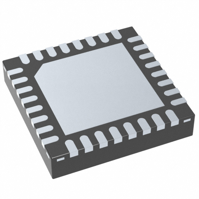


 工商网监
湘ICP备2023018690号
工商网监
湘ICP备2023018690号


