TFP401A-EP
SLDS160A – MARCH 2009 – REVISED JULY 2011
www.ti.com
TI PanelBus™ DIGITAL RECEIVER
Check for Samples: TFP401A-EP
FEATURES
1
•
2
•
•
•
•
•
•
•
•
•
•
(1)
(2)
(3)
Supports Pixel Rates Up to 165 MHz (including
1080p and WUXGA at 60Hz)
Digital Visual Interface (DVI) Specification
Compliant (1)
True-Color, 24 Bit/Pixel, 16.7M Colors at One
or Two Pixels Per Clock
Laser Trimmed Internal Termination Resistors
for Optimum Fixed Impedance Matching
Skew Tolerant Up to One Pixel Clock Cycle
4x Over-Sampling
Reduced Power Consumption - 1.8 V Core
Operation With 3.3 V I/Os and Supplies (2)
Reduced Ground Bounce Using
Time-Staggered Pixel Outputs
Low Noise and Power Dissipation Using TI
PowerPAD™ Packaging
Advanced Technology Using TI 0.18-mm
EPIC-5™ CMOS Process
TFP401A Incorporates HSYNC Jitter
Immunity (3)
The Digital Visual Interface Specification, DVI, is an industry
standard developed by the Digital Display Working Group
(DDWG) for high-speed digital connection to digital displays.
The TFP401A is compliant to the DVI Specification Rev. 1.0.
The TFP401A has an internal voltage regulator that provides
the 1.8-V core power supply from the externally supplied
3.3-V supplies.
The TFP401A incorporates additional circuitry to create a
stable HSYNC from DVI transmitters that introduce
undesirable jitter on the transmitted HSYNC signal.
SUPPORTS DEFENSE, AEROSPACE,
AND MEDICAL APPLICATIONS
•
•
•
•
•
•
•
Controlled Baseline
One Assembly/Test Site
One Fabrication Site
Available in Military (–55°C/125°C)
Temperature Range (Custom temperature
ranges available)
Extended Product Life Cycle
Extended Product-Change Notification
Product Traceability
DESCRIPTION
The Texas Instruments TFP401A is a TI PanelBus ™
flat panel display product, part of a comprehensive
family of end-to-end DVI 1.0 compliant solutions.
Targeted primarily at desktop LCD monitors and
digital projectors, the TFP401A finds applications in
any design requiring high-speed digital interface. The
TFP401A supports display resolutions up to 1080p
and WUXGA in 24-bit true color pixel format. The
TFP401A offers design flexibility to drive one or two
pixels per clock, supports TFT or DSTN panels, and
provides an option for time staggered pixel outputs
for reduced ground bounce. PowerPAD™ advanced
packaging technology results in best of class power
dissipation,
footprint,
and
ultra-low
ground
inductance. The TFP401A combines PanelBus ™
circuit innovation with TI's advanced 0.18-mm
EPIC-5™ CMOS process technology, along with TI
PowerPAD™ package technology to achieve a
reliable, low-powered, low-noise, high-speed digital
interface solution.
1
2
Please be aware that an important notice concerning availability, standard warranty, and use in critical applications of Texas
Instruments semiconductor products and disclaimers thereto appears at the end of this data sheet.
PanelBus, PowerPAD, EPIC-5 are trademarks of Texas Instruments.
PRODUCTION DATA information is current as of publication date.
Products conform to specifications per the terms of the Texas
Instruments standard warranty. Production processing does not
necessarily include testing of all parameters.
Copyright © 2009–2011, Texas Instruments Incorporated
�TFP401A-EP
SLDS160A – MARCH 2009 – REVISED JULY 2011
www.ti.com
ORDERING INFORMATION (1)
PACKAGED DEVICE (2)
(1)
(2)
TA
100-TQFP
(PZP)
–55°C to 125°C
TFP401AMPZPEP
For the most current package and ordering information, see the Package Option Addendum at the end of this document, or see the TI
Web site at www.ti.com.
Package drawings, standard packing quantities, thermal data, symbolization, and PCB design guidelines are available at
www.ti.com/sc/package.
OGND
QO23
OVDD
AGND
Rx2+
Rx2−
AVDD
AGND
AVDD
Rx1+
Rx1−
AGND
AVDD
AGND
Rx0+
Rx0−
AGND
RxC+
RxC−
AVDD
75
74
73
72
71
70
69
68
67
66
65
64
63
62
61
60
59
58
57
56
55
54
53
52
51
QO22
QO21
QO20
QO19
QO18
QO17
QO16
GND
DVDD
QO15
QO14
QO13
QO12
QO11
QO10
QO9
QO8
OGND
OVDD
QO7
QO6
QO5
QO4
QO3
QO2
100-PIN PACKAGE
(TOP VIEW)
RSVD
OCK_INV
99
100
50
49
48
47
46
45
44
43
42
41
40
39
38
37
36
35
34
33
32
31
30
29
28
27
26
QO1
QO0
HSYNC
VSYNC
DE
OGND
ODCK
OVDD
CTL3
CTL2
CTL1
GND
DVDD
QE23
QE22
QE21
QE20
QE19
QE18
QE17
QE16
OVDD
OGND
QE15
QE14
DFO
PD
ST
PIXS
GND
DVDD
STAG
SCDT
PDO
QE0
QE1
QE2
QE3
QE4
QE5
QE6
QE7
OVDD
OGND
QE8
QE9
QE10
QE11
QE12
QE13
1
2
3
4
5
6
7
8
9
10
11
12
13
14
15
16
17
18
19
20
21
22
23
24
25
EXT_RES
PVDD
PGND
76
77
78
79
80
81
82
83
84
85
86
87
88
89
90
91
92
93
94
95
96
97
98
2
Copyright © 2009–2011, Texas Instruments Incorporated
�TFP401A-EP
SLDS160A – MARCH 2009 – REVISED JULY 2011
www.ti.com
FUNCTIONAL BLOCK DIAGRAM
3.3 V
3.3 V
1.8 V
Regulator
Internal 50-Ω
Termination
3.3 V
RED(0-7)
Rx2+
Rx2-
+
_
Channel 2
CH2(0-9)
Latch
CTL2
Channel 1
Rx1+
Rx1-
+
_
Latch
Rx0+
Rx0-
+
_
Latch
RxC+
RxC-
+
_
PLL
QE(0-23)
QO(0-23)
CTL3
Data Recovery CH1(0-9)
TMDS
and
Decoder
Synchronization
Channel 0
CH0(0-9)
GRN(0-7)
CTL1
Panel
Interface
BLU(0-7)
VSYNC
HSYNC
ODCK
DE
SCDT
CTL3
CTL2
CTL1
VSYNC
HSYNC
TERMINAL FUNCTIONS
TERMINAL
I/O
DESCRIPTION
NAME
NO.
AGND
79, 83, 87, 89, 92
GND
Analog Ground - Ground reference and current return for analog circuitry.
AVDD
82, 84, 88, 95
VDD
Analog VDD - Power supply for analog circuitry. Nominally 3.3 V
42, 41, 40
DO
General-purpose control signals - Used for user defined control. CTL1 is not powered-down
via PDO.
DO
Output data enable - Used to indicate time of active video display versus non-active display
or blank time. During blank, only HSYNC, VSYNC, and CTL1-3 are transmitted. During times
of active display, or non-blank, only pixel data, QE[23:0] and QO[23:0], is transmitted.
High : Active display time
Low: Blank time
1
DI
Output clock data format - Controls the output clock (ODCK) format for either TFT or DSTN
panel support. For TFT support ODCK clock runs continuously. For DSTN support ODCK
only clocks when DE is high, otherwise ODCK is held low when DE is low.
High : DSTN support/ODCK held low when DE = low
Low: TFT support/ODCK runs continuously.
DGND
5, 39, 68
GND
Digital ground - Ground reference and current return for digital core
DVDD
6, 38, 67
VDD
Digital VDD - Power supply for digital core. Nominally 3.3 V
EXT_RES
96
AI
Internal impedance matching - The TFP401A is internally optimized for impedance matching
at 50 W. An external resistor tied to this pin has no effect on device performance.
HSYNC
48
DO
Horizontal sync output
RSVD
99
DI
Reserved. Must be tied high for normal operation.
OVDD
18, 29, 43, 57, 78
VDD
Output driver VDD - Power supply for output drivers. Nominally 3.3 V
ODCK
44
DO
Output data clock - Pixel clock. All pixel outputs QE[23:0] and QO[23:0] (if in 2-pixel/clock
mode) along with DE, HSYNC, VSYNC and CTL[3:1] are synchronized to this clock.
OGND
19, 28 ,45, 58, 76
GND
CTL[3:1]
DE
DFO
OCK_INV
46
100
DI
Output driver ground - Ground reference and current return for digital output drivers
ODCK Polarity - Selects ODCK edge on which pixel data (QE[23:0] and QO[23:0]) and
control signals (HSYNC, VSYNC, DE, CTL1-3 ) are latched.
Normal Mode:
High : Latches output data on rising ODCK edge
Low : Latches output data on falling ODCK edge
Copyright © 2009–2011, Texas Instruments Incorporated
3
�TFP401A-EP
SLDS160A – MARCH 2009 – REVISED JULY 2011
www.ti.com
TERMINAL FUNCTIONS (continued)
TERMINAL
NAME
PD
NO.
2
I/O
DESCRIPTION
DI
Power down - An active low signal that controls the TFP401A power-down state. During
power down all output buffers are switched to a high impedance state. All analog circuits are
powered down and all inputs are disabled, except for PD.
If PD is left unconnected an internal pullup defaults the TFP401A to normal operation.
High : Normal operation
Low: Power down
Output drive power down - An active low signal that controls the power-down state of the
output drivers. During output drive power down, the output drivers (except SCDT and CTL1)
are driven to a high impedance state. When PDO is left unconnected, an internal pullup
defaults the TFP401A to normal operation.
High : Normal operation/output drivers on
Low: Output drive power down.
PDO
9
DI
PGND
98
GND
PLL GND - Ground reference and current return for internal PLL
Pixel select - Selects between one or two pixels per clock output modes. During the
2-pixel/clock mode, both even pixels, QE[23:0], and odd pixels, QO[23:0], are output in
tandem on a given clock cycle. During 1-pixel/clock, even and odd pixels are output
sequentially, one at a time, with the even pixel first, on the even pixel bus, QE[23:0]. (The
first pixel per line is pixel-0, the even pixel. The second pixel per line is pixel-1, the odd
pixel).
High : 2-pixel/clock
Low: 1-pixel/clock
PIXS
4
DI
PVDD
97
VDD
PLL VDD - Power supply for internal PLL
DO
Even green pixel output - Output for even and odd green pixels when in 1-pixel/clock mode.
Output for even only green pixel when in 2-pixel/clock mode. Output data is synchronized to
the output data clock, ODCK.
LSB: QE8/pin 20
MSB: QE15/pin 27
DO
Even red pixel output - Output for even and odd red pixels when in 1-pixel/clock mode.
Output for even only red pixel when in 2-pixel/clock mode. Output data is synchronized to the
output data clock, ODCK.
LSB: QE16/pin 30
MSB: QE23/pin 37
DO
Odd blue pixel output - Output for odd only blue pixel when in 2-pixel/clock mode. Not used,
and held low, when in 1-pixel/clock mode. Output data is synchronized to the output data
clock, ODCK.
LSB: QO0/pin 49
MSB: QO7/pin 56
DO
Odd green pixel output - Output for odd only green pixel when in 2-pixel/clock mode. Not
used, and held low, when in 1-pixel/clock mode. Output data is synchronized to the output
data clock, ODCK.
LSB: QO8/pin 59
MSB: QO15/pin 66
DO
Odd red pixel output - Output for odd only red pixel when in 2-pixel/clock mode. Not used,
and held low, when in 1-pixel/clock mode. Output data is synchronized to the output data
clock, ODCK.
LSB: QO16/pin 69
MSB: QO23/pin 77
10-17
DO
Even blue pixel output - Output for even and odd blue pixels when in 1-pixel/clock mode.
Output for even only blue pixel when in 2-pixel per clock mode. Output data is synchronized
to the output data clock, ODCK.
LSB: QE0/pin 10
MSB: QE7/pin 17
RxC+
93
AI
Clock positive receiver input - Positive side of reference clock. TMDS low voltage signal
differential input pair.
RxC-
94
AI
Clock negative receiver input - Negative side of reference clock. TMDS low voltage signal
differential input pair.
AI
Channel-0 positive receiver input - Positive side of channel-0. TMDS low voltage signal
differential input pair.
Channel-0 receives blue pixel data in active display and HSYNC, VSYNC control signals in
blank.
QE[8:15]
QE[16:23]
QO[0:7]
QO[8:15]
QO[16:23]
QE[0:7]
Rx0+
4
20-27
30-37
49-56
59-66
69-75, 77
90
Copyright © 2009–2011, Texas Instruments Incorporated
�TFP401A-EP
SLDS160A – MARCH 2009 – REVISED JULY 2011
www.ti.com
TERMINAL FUNCTIONS (continued)
TERMINAL
NAME
NO.
I/O
DESCRIPTION
Rx0-
91
AI
Channel-0 negative receiver input - Negative side of channel-0. TMDS low voltage signal
differential input pair.
Rx1+
85
AI
Channel-1 positive receiver input - Positive side of channel-1 TMDS low voltage signal
differential input pair.
Channel-1 receives green pixel data in active display and CTL1 control signals in blank.
Rx1-
86
AI
Channel-1 negative receiver input - Negative side of channel-1 TMDS low voltage signal
differential input pair.
Rx2+
80
AI
Channel-2 positive receiver input - Positive side of channel-2 TMDS low voltage signal
differential input pair.
Channel-2 receives red pixel data in active display and CTL2, CTL3 control signals in blank.
Rx2-
81
AI
Channel-2 negative receiver input - Negative side of channel-2 TMDS low voltage signal
differential input pair.
SCDT
8
DO
Sync detect - Output to signal when the link is active or inactive. The link is considered to be
active when DE is actively switching. The TFP401A monitors the state DE to determine link
activity. SCDT can be tied externally to PDO to power down the output drivers when the link
is inactive.
High: Active link
Low: Inactive link
ST
3
DI
Output drive strength select - Selects output drive strength for high or low current drive. (See
dc specifications for IOH and IOL vs ST state).
High : High drive strength
Low : Low drive strength
STAG
7
DI
Staggered pixel select - An active low signal used in the 2-pixel/clock pixel mode
(PIXS = high). Time staggers the even and odd pixel outputs to reduce ground bounce.
Normal operation outputs the odd and even pixels simultaneously.
High : Normal simultaneous even/odd pixel output
Low: Time staggered even/odd pixel output
VSYNC
47
DO
Vertical sync output
ABSOLUTE MAXIMUM RATINGS (1)
over operating free-air temperature range (unless otherwise noted)
MIN
MAX
DVDD, AVDD, OVDD, PVDD
Supply voltage range
-0.3
4
VI
Input voltage range, logic/analog signals
-0.3
4
V
Operating ambient temperature range
-55
125
°C
Tstg
Storage temperature range (2)
–65
150
°C
Tc
Case temperature for 10 seconds
260
°C
Lead temperature 1,6 mm (1/16 inch) from case for 10 seconds
260
°C
Package power dissipation/ PowerPAD™
ESD protection, all pins
JEDEC latchup (EIA/JESD78)
(1)
(2)
(3)
(4)
Soldered
(3)
Not soldered (4)
4.3
2.7
UNIT
V
W
25
KV
Human
Body
Model
100
mA
Stresses beyond those listed under "absolute maximum ratings" may cause permanent damage to the device. These are stress ratings
only, and functional operation of the device at these or any other conditions beyond those indicated under "recommended operating
conditions" is not implied. Exposure to absolute-maximum-rated conditions for extended periods may affect device reliability.
Long-term high–temperature storage and/or extended use at maximum recommended operating conditions may result in a reduction of
overall device life. See http://www.ti.com/ep_quality for additional information on enhanced plastic packaging
Specified with PowerPAD™ bond pad on the backside of the package soldered to a 2 oz. Cu plate PCB thermal plane. Specified at
maximum allowed operating temperature, 70°C.
PowerPAD™ bond pad on the backside of the package is not soldered to a thermal plane. Specified at maximum allowed operating
temperature, 70°C.
Copyright © 2009–2011, Texas Instruments Incorporated
5
�TFP401A-EP
SLDS160A – MARCH 2009 – REVISED JULY 2011
www.ti.com
RECOMMENDED OPERATING CONDITIONS
over operating free-air temperature range (unless otherwise noted)
VDD (DVDD, AVDD, PVDD, OVDD) Supply voltage
tpix
(1)
Pixel time
NOM
MAX
3
3.3
3.6
V
40
ns
6.06
Rt
Single ended analog input termination resistance
TA
Operating free-air temperature
(1)
MIN
45
50
-55
UNIT
57
Ω
125
°C
tpix is the pixel time defined as the period of the RxC clock input. The period of the output clock, ODCK is equal to tpix when in
1-pixel/clock mode and 2tpix when in 2-pixel/clock mode.
DC DIGITAL I/O ELECTRICAL CHARACTERISTICS
over operating free-air temperature range (unless otherwise noted)
MAX
UNIT
VIH
High level digital input voltage (1)
PARAMETER
2
DVDD
V
VIL
Low level digital input voltage (1)
0
0.8
V
IOH
High level output drive current (2)
Low level output drive current (2)
IOL
IOZ
(1)
(2)
TEST CONDITIONS
Hi-Z output leakage current
MIN
TYP
ST = High,
VOH =2.4
V
5
10
16.3
ST = Low,
VOH = 2.4
V
3
6
10.3
ST = High,
VOL = 0.8
V
8
13
19
ST = Low,
VOL = 0.8
V
4
7
11
PD = Low or PDO = Low
-1
1
mA
mA
μA
Digital inputs are labeled DI in I/O column of Terminal Functions Table.
Digital outputs are labeled DO in I/O column of Terminal Functions Table.
DC ELECTRICAL CHARACTERISTICS
over operating free-air temperature range (unless otherwise noted)
PARAMETER
TEST CONDITIONS
VID
Analog input differential voltage (1)
VIC
Analog input common mode voltage (1)
VI(OC)
Open circuit analog input voltage
IDD(2PIX)
Normal 2-pix/clock power supply
current (2)
IPD
Power down current
IPDO
(1)
(2)
(3)
6
MAX
UNIT
75
TYP
1200
mV
AVDD-300
AVDD-37
mV
AVDD-10
AVDD+10
mV
ODCK = 82.5 MHz
2-pix/clock
(3)
Output drive power down current
MIN
370
PD = Low
(3)
10
PDO = Low
35
mA
mA
mA
Specified as dc characteristic with no overshoot or undershoot.
Alternating 2-pixel black/2-pixel white pattern. ST = high, STAG = high, QE[23:0] and QO[23:0] CL = 10 pF.
Analog inputs are open circuit (transmitter is disconnected from TFP401A).
Copyright © 2009–2011, Texas Instruments Incorporated
�TFP401A-EP
SLDS160A – MARCH 2009 – REVISED JULY 2011
www.ti.com
AC ELECTRICAL CHARACTERISTICS
over operating free-air temperature range (unless otherwise noted)
PARAMETER
TEST CONDITIONS
(1)
MIN
TYP
UNIT
1560
mVp-p
VID(2)
Differential input sensitivity
tps
Analog input intra-pair (+ to -)
differential skew (2)
tccs
Analog Input inter-pair or
channel-to-channel skew
tijit
Worse case differential input clock
jitter tolerance (5), (2) (6)
tf1
Fall time of data and control
signals (7), (8) (6)
ST = Low,
CL=5 pF
2.4
ST = High,
CL=10 pF
1.9
Rise time of data and control
signals (7), (8) (6)
ST = Low,
CL=5 pF
2.4
ST = High,
CL=10 pF
1.9
Rise time of ODCK clock (7)
ST = Low,
CL=5 pF
2.4
ST = High,
CL=10 pF
1.9
ST = Low,
CL=5 pF
2.4
ST = High,
CL=10 pF
1.9
tr1
tr2
tsu1
1
(6)
(6)
Hold time, data and control signal to
falling edge of ODCK (6)
tsu2
Hold time, data and control signal to
rising edge of ODCK (6)
fODCK
ODCK frequency
ODCK duty-cycle
tpd(PDL)
Propagation delay time from PD low
to Hi-Z outputs (6)
tbit
(3)
tpix
(4)
ps
ns
ns
ns
ns
1.8
2 pixel/clock, PIXS = high,
STAG = high, OCK_INV = low
3.8
2 pixel and STAG, PIXS = high,
STAG = low, OCK_INV = low
0.6
1 pixel/clock, PIXS = low,
OCK_INV = low
0.6
2 pixel and STAG, PIXS = high,
STAG = low, OCK_INV = low
2.5
2 pixel/clock, PIXS = high,
STAG = high, OCK_INV = low
2.9
Setup time, data and control signal to 1 pixel/clock, PIXS = low,
rising edge of ODCK (6)
OCK_INV = high
th2
(5)
(6)
(7)
(8)
50
Setup time, data and control signal to 1 pixel/clock, PIXS = low,
falling edge of ODCK (6)
OCK_INV = low
th1
(1)
(2)
(3)
(4)
0.4
(2)
Fall time of ODCK clock (7)
tf2
150
MAX
ns
ns
2.1
2 pixel/clock, PIXS = high,
STAG = high, OCK_INV = high
4
2 pixel and STAG, PIXS = high,
STAG = low, OCK_INV = high
1.5
1 pixel/clock, PIXS = low,
OCK_INV = high
0.3
2 pixel and STAG, PIXS = high,
STAG = low, OCK_INV = high
2.4
2 pixel/clock, PIXS = high,
STAG = high, OCK_INV = high
2.1
PIX = Low (1-PIX/CLK)
25
165
PIX = High (2-PIX/CLK)
12.5
82.5
45%
ns
ns
60%
MHz
75%
9
ns
Specified as ac parameter to include sensitivity to overshoot, undershoot and reflection.
By characterization
tbit is 1/10 the pixel time, tpix
tpix is the pixel time defined as the period of the RxC input clock. The period of ODCK is equal to tpix in 1-pixel/clock mode or 2tpix when
in 2-pixel/clock mode.
Measured differentially at 50% crossing using ODCK output clock as trigger.
Not Production Test
Rise and fall times measured as time between 20% and 80% of signal amplitude.
Data and control signals are : QE[23:0], QO[23:0], DE, HSYNC, VSYNC and CTL[3:1]
Copyright © 2009–2011, Texas Instruments Incorporated
7
�TFP401A-EP
SLDS160A – MARCH 2009 – REVISED JULY 2011
www.ti.com
AC ELECTRICAL CHARACTERISTICS (continued)
over operating free-air temperature range (unless otherwise noted)
PARAMETER
TEST CONDITIONS
MIN
TYP
tpd(PDOL)
Propagation delay time from PDO low
to Hi-Z outputs (6)
tt(HSC)
Transition time between DE transition
to SCDT low (9)
~17-26
tt(FSC)
Transition time between DE transition
to SCDT high (9)
8
td(st)
Delay time, ODCK latching edge to
QE[23:0] data output
(9)
8
MAX
9
STAG = Low
PIXS = High
0.25
UNIT
ns
ms
DE
transitions
tpix
(4)
Link active or inactive is determined by amount of time detected between DE transitions. SCDT indicates link activity.
Copyright © 2009–2011, Texas Instruments Incorporated
�TFP401A-EP
SLDS160A – MARCH 2009 – REVISED JULY 2011
www.ti.com
PARAMETER MEASUREMENT INFORMATION
tr1
tf1
80%
QE(0-23), QO(0-23), DE
CTK(1-3), HSYNC, VSYNC
80%
20%
20%
Figure 1. Rise and Fall TIme of Data and Control Signals
tr2
tf2
80%
ODCK
80%
20%
20%
Figure 2. Rise and Fall Time of ODCK
fODCK
ODCK
Figure 3. ODCK Frequency
t(su2)
t(su1)
t(h2)
t(h1)
VOH
VOL
ODCK
VOH
VOL
QE(0-23), QO(0-23), DE
CTL(1-3), HSYNC, VSYNC
VOH
VOL
VOH
VOL
VOH
VOL
VOH
VOL
OCK_INV
Figure 4. Data Setup and Hold Time to Rising and Falling Edge of ODCK
VOH
ODCK
td(st)
QE(O-23)
50%
Figure 5. ODCK High to QE[23:0] Staggered Data Output
Figure 6. Analog Input Intra-Pair Differential Skew
PD
VIL
tpd(PDL)
QE(0-23), QO(0-23),
ODCK, DE, CTL(1-3),
HSYNC, VSYNC, SCDT
Figure 7. Delay from PD Low to Hi-Z Outputs
Copyright © 2009–2011, Texas Instruments Incorporated
9
�TFP401A-EP
SLDS160A – MARCH 2009 – REVISED JULY 2011
www.ti.com
PARAMETER MEASUREMENT INFORMATION (continued)
PDO
VIL
tpd(PDOL)
QE(0-23), QO(0-23),
ODCK, DE, CTL(2-3),
HSYNC, VSYNC
Figure 8. Delay from PDO Low to Hi-Z Outputs
VIH
PD
tp(PDH-V)
DFO, ST, PIXS, STAG,
Rx(0-2)+, Rx(0-2)-,
OCK_INV
Figure 9. Delay from PD Low to High Before Inputs are Active
twL(PDL_MIN)
VIL
PD
Figure 10. Minimum Time PD Low
TX2
50%
TX1
tccs
TX0
50%
Figure 11. Analog Input Channel-to-Channel Skew
tt(HSC)
tt(FSC)
DE
SCDT
Figure 12. Time Between DE Transitions to SCDT Low and SCDT High
tDEL
tDEH
DE
Figure 13. Minimum DE Low and Maximum DE High
10
Copyright © 2009–2011, Texas Instruments Incorporated
�TFP401A-EP
SLDS160A – MARCH 2009 – REVISED JULY 2011
www.ti.com
FUNDAMENTAL OPERATION
The TFP401A is a digital visual interface (DVI) compliant TMDS digital receiver that is used in digital flat panel
display systems to receive and decode TMDS encoded RGB pixel data streams. In a digital display system a
host, usually a PC or workstation, contains a TMDS compatible transmitter that receives 24 bit pixel data along
with appropriate control signals and encodes them into a high-speed low-voltage differential serial bit stream fit
for transmission over a twisted-pair cable to a display device. The display device, usually a flat-panel monitor, will
require a TMDS compatible receiver like the TI TFP401A to decode the serial bit stream back to the same 24 bit
pixel data and control signals that originated at the host. This decoded data can then be applied directly to the
flat panel drive circuitry to produce an image on the display. Since the host and display can be separated by
distances up to 5 meters or more, serial transmission of the pixel data is preferred. To support modern display
resolutions up to UXGA a high bandwidth receiver with good jitter and skew tolerance is required.
TMDS PIXEL DATA AND CONTROL SIGNAL ENCODING
TMDS stands for transition minimized differential signaling. Only one of two possible TMDS characters for a
given pixel will be transmitted at a given time. The transmitter keeps a running count of the number of ones and
zeros previously sent and transmits the character that will minimize the number of transitions and approximate a
dc balance of the transmission line. Three TMDS channels are used to receive RGB pixel data during active
display time, DE = high. The same three channels also receive control signals, HSYNC, VSYNC, and user
defined control signals CTL[3:1]. These control signals are received during inactive display or blanking-time.
Blanking-time is when DE = low. The following table maps the received input data to appropriate TMDS input
channel in a DVI compliant system.
RECEIVED PIXEL DATA
ACTIVE DISPLAY DE = HIGH
INPUT CHANNEL
OUTPUT PINS
(VALID FOR DE = HIGH)
Red[7:0]
Channel - 2 (Rx2 +)
QE[23:16] QO[23:16]
Green[7:0]
Channel - 1 (Rx1 +)
QE[15:8] QO[15:8]
Blue[7:0]
Channel - 0 (Rx0 +)
QE[7:0] QO[7:0]
RECEIVED CONTROL DATA
BLANKING DE = LOW
INPUT CHANNEL
UTPUT PINS
(VALID FOR DE = LOW)
CTL[3:2]
Channel - 2 (Rx2 +)
CTL[3:2]
CTL[1: 0]
(1)
HSYNC, VSYNC
(1)
Channel - 1 (Rx1 +)
CTL1
Channel - 0 (Rx0 +)
HSYNC, VSYNC
Some TMDS transmitters transmit a CTL0 signal. The TFP401A decodes and transfers CTL[3:1] and ignores CTL0 characters. CTL0 is
not available as a TFP401A output.
The TFP401A discriminates between valid pixel TMDS characters and control TMDS characters to determine the
state of active display versus blanking, i.e., state of DE.
Copyright © 2009–2011, Texas Instruments Incorporated
11
�TFP401A-EP
SLDS160A – MARCH 2009 – REVISED JULY 2011
www.ti.com
TFP401A CLOCKING AND DATA SYNCHRONIZATION
The TFP401A receives a clock reference from the DVI transmitter that has a period equal to the pixel time, Tpix.
The frequency of this clock is also referred to as the pixel rate. Since the TMDS encoded data on Rx[2:0]
contains 10 bits per 8-bit pixel, it follows that the Rx[2:0] serial bit rate is 10 times the pixel rate. For example, the
required pixel rate to support an UXGA resolution with 60-Hz refresh rate is 165 MHz. The TMDS serial bit rate is
10x the pixel rate or 1.65 Gb/s. Due to the transmission of this high-speed digital bit stream, on three separate
channels (or twisted-pair wires) of long distances (3-5 meters), phase synchronization between the data steams
and the input reference clock is not specified. In addition, skew between the three data channels is common. The
TFP401A uses a 4x oversampling scheme of the input data streams to achieve reliable synchronization with up
to 1-Tpix channel-to-channel skew tolerance. Accumulated jitter on the clock and data lines due to reflections
and external noise sources is also typical of high speed serial data transmission, hence the TFP401A's design
for high jitter tolerance.
The input clock to the TFP401A is conditioned by a phase-locked-loop (PLL) to remove high-frequency jitter from
the clock. The PLL provides four 10x clock outputs of different phase to locate and sync the TMDS data streams
(4x oversampling). During active display the pixel data is encoded to be transition minimized, whereas in blank,
the control data is encoded to be transition maximized. A DVI compliant transmitter is required to transmit in
blank for a minimum period of time, 128-Tpix, to specify sufficient time for data synchronization when the receiver
sees a transition maximized code. Synchronization during blank, when the data is transition maximized, specifies
reliable data bit boundary detection. Phase synchronization to the data streams is unique for each of the three
input channels and is maintained as long as the link remains active.
TFP401A TMDS INPUT LEVELS AND INPUT IMPEDANCE MATCHING
The TMDS inputs to the TFP401A receiver have a fixed single-ended termination to AVDD The TFP401A is
internally optimized using a laser trim process to precisely fix the impedance at 50 W. The device functions
normally with or without a resistor on the EXT_RES pin, so it remains drop-in compatible with current sockets.
The fixed impedance eliminates the need for an external resistor while providing optimum impedance matching
to standard 50-W DVI cables.
Figure 14 shows a conceptual schematic of a DVI transmitter and TFP401A receiver connection. A transmitter
drives the twisted pair cable via a current source, usually achieved with an open-drain type output driver. The
internal resistor, which is matched to the cable impedance, at the TFP401A input provides a pullup to AVDD .
Naturally, when the transmitter is disconnected and the TFP401A DVI inputs are left unconnected, the TFP401A
receiver inputs pullup to AVDD. The single ended differential signal and full differential signal is shown in
Figure 15. The TFP401A is designed to respond to differential signal swings ranging from 150 mV to 1.56 V with
common mode voltages ranging from (AVDD-300 mV) to (AVDD-37 mV).
12
Copyright © 2009–2011, Texas Instruments Incorporated
�TFP401A-EP
SLDS160A – MARCH 2009 – REVISED JULY 2011
www.ti.com
DVI
Transmitter
TI TFP401/401A
Receiver
AVDD
DVI Compliant Cable
Internal Termination
at 50 Ω
DATA
DATA
+
_
Current
Source
Figure 14. TMDS Differential Input and Transmitter Connection
1/2 VIDIFF
AVCC
AVCC - 1/2 VIDIFF
a ) Single-Ended Input Signal
VIDIFF
+ 1/2 VIDIFF
- 1/2 VIDIFF
b) Differential Input Signal
Figure 15. TMDS Inputs
TFP401A INCORPORATES HSYNC JITTER IMMUNITY
Several DVI transmitters available in the market introduce jitter on the transmitted HSYNC and VSYNC signals
during the TMDS encryption process. The HSYNC signal can shift by one pixel position (one clock) from nominal
in either direction, resulting in up to two cycles of HSYNC shift. This jitter carries through to the DVI receiver, and
if the position of HSYNC shifts continuously, the receiver can lose track of the input timing and pixel noise will
occur on the display. For this reason, a DVI compliant receiver with HSYNC jitter immunity should be used in all
displays that could be connected to host PCs with transmitters that have this HSYNC jitter problem.
The TFP401A integrates HSYNC regeneration circuitry that provides a seamless interface to these noncompliant
transmitters. The position of the data enable (DE) signal is always fixed in relation to data, irrespective of the
location of HSYNC. The TFP401A receiver uses the DE and clock signals recreate stable vertical and horizontal
sync signals. The circuit filters the HSYNC output of the receiver, and HSYNC is shifted to the nearest eighth bit
boundary, producing a stable output with respect to data, as shown in Figure 16. This will ensure accurate data
synchronization at the input of the display timing controller.
Copyright © 2009–2011, Texas Instruments Incorporated
13
�TFP401A-EP
SLDS160A – MARCH 2009 – REVISED JULY 2011
www.ti.com
This HSYNC regeneration circuit is transparent to the monitor and need not be removed even if the transmitted
HSYNC is stable. For example, the PanelBus ™ line of DVI 1.0 compliant transmitters, such as the TFP6422 and
TFP420, do not have the HSYNC jitter problem. The TFP401A will operate correctly with either compliant or
noncompliant transmitters. In contrast, the TFP401 is ideal for customers who have control over the transmit
portion of the design such as bundled system manufacturers and for internal monitor use (the DVI connection
between monitor and panel modules).
ODCK
HSYNC Shift by ± 1 Clock
HSYNC IN
DE
HSYNC OUT
Figure 16. HSYNC Regeneration Timing Diagram
TFP401A MODES OF OPERATION
The TFP401A provides systems design flexibility and value by providing the system designer with configurable
options or modes of operation to support varying system architectures. The following table outlines the various
panel modes that can be supported along with appropriate external control pin settings.
PANEL
PIXEL RATE
ODCK LATCH
EDGE
ODCK
DFO
PIXS
OCK_INV
TFT or 16-bit
DSTN
1 pix/clock
Falling
Free run
0
0
0
TFT or 16-bit
DSTN
1 pix/clock
Rising
Free run
0
0
1
TFT
2 pix/clock
Falling
Free run
0
1
0
TFT
2 pix/clock
Rising
Free run
0
1
1
24-bit DSTN
1 pix/clock
Falling
Gated low
1
0
0
NONE
1 pix/clock
Rising
Gated low
1
0
1
24-bit DSTN
2 pix/clock
Falling
Gated low
1
1
0
24-bit DSTN
2 pix/clock
Rising
Gated low
1
1
1
TFP401A OUTPUT DRIVER CONFIGURATIONS
The TFP401A provides flexibility by offering various output driver features that can be used to optimize power
consumption, ground-bounce and power-supply noise. The following sections outline the output driver features
and their effects.
Output driver power down (PDO = low), Pulling PDO low will place all the output drivers, except CTL1 and
SCDT, into a high-impedance state. The SCDT output which indicates link-disabled or link-inactive can be tied
directly to the PDO input to disable the output drivers when the link is inactive or when the cable is disconnected.
An internal pullup on the PDO pin will default the TFP401A to the normal nonpower down output drive mode if
left unconnected.
Drive Strength (ST = high for high drive strength, ST=low for low drive strength.) The TFP401A allows for
selectable output drive strength on the data, control and ODCK outputs. See the dc specifications table for the
values of IOH and IOL current drives for a given ST state. The high output strength offers approximately two
times the drive as the low output drive strength.
14
Copyright © 2009–2011, Texas Instruments Incorporated
�TFP401A-EP
www.ti.com
SLDS160A – MARCH 2009 – REVISED JULY 2011
Time Staggered Pixel Output. This option works only in conjunction with the 2-pixel/clock mode (PIXS = high).
Setting STAG = low will time stagger the even and odd pixel output so as to reduce the amount of instantaneous
current surge from the power supply. Depending on the PCB layout and design this can help reduce the amount
of system ground bounce and power supply noise. The time stagger is such that in 2-pixel/clock mode the even
pixel is delayed from the latching edge of ODCK by 0.25 Tcip. (Tcip is the period of ODCK. The ODCK period is
2Tpix when in 2-pixel/clock mode.)
Depending on system constraints of output load, pixel rate, panel input architecture and board cost the TFP401A
drive strength and staggered pixel options allow flexibility to reduce system power-supply noise, ground bounce
and EMI.
Power Management. The TFP401A offers several system power management features.
The output driver power down (PDO = low) is an intermediate mode which offers several uses. During this mode,
all output drivers except SCDT and CTL1 are driven to a high-impedance state while the rest of the device
circuitry remains active
The TFP401A power down (PD = low) is a complete power down in that it powers down the digital core, the
analog circuitry, and output drivers. All output drivers are placed into a Hi-Z state. All inputs are disabled except
for the PD input. The TFP401A will not respond to any digital or analog inputs until PD is pulled high.
Both PDO and PD have internal pullups, so if left unconnected they default the TFP401A to normal operating
modes.
Sync Detect. The TFP401A offers an output, SCDT, to indicate link activity. The TFP401A monitors activity on
DE to determine if the link is active. When 2^18 clocks produced by an on-chip free running oscillator whose
frequency is around 10-15 MHz pass without a transition on DE, the TFP401A considers the link inactive and
SCDT is driven low. Hence SCDT goes low after the terminal count of the counter is reached that is 17~26 ms.
When SCDT is low, if 8 DE edges are detected within the terminal count of 2^18 clocks, the link is considered
active and SCDT goes high.
SCDT can be used to signal a system power management circuit to initiate a system power down when the link
is considered inactive. The SCDT can also be tied directly to the TFP401A PDO input to power down the output
drivers when the link is inactive. It is not recommended to use the SCDT to drive the PD input since, once in
complete power-down, the analog inputs are ignored and the SCDT state does not change. An external system
power management circuit to drive PD is preferred.
SYNC DETECT OPERATION
Some graphics card when in sleep/standby mode send characters that can make the DE toggle and make SCDT
high, hence in such applications, to robustly determine if the link is in active or inactive mode, it is recommended
that a sync signal like HSYNC can be used in addition to the SCDT. Timing format on the recovered HSYNC
signal can be used in addition to SCDT to determine if the link is receiving a valid video format.
In applications where PD is being pulsed (to save power while in sleep/standby mode) when the link is inactive,
and SCDT is used solely to determine the link activity, then in such cases SCDT should not be used until 25 ms
of signal and power application.
There is a rare possibility that SCDT can get stuck high on power up or removal of the DVI signal. For example:
If the power on a DVI distribution box sourcing the signal to the receiver is cycled rapidly (2-3 times/second),
then there is a small possibility, (1 in ~40-50 times) of cycling power that SCDT may be stuck high when the box
is powered off.
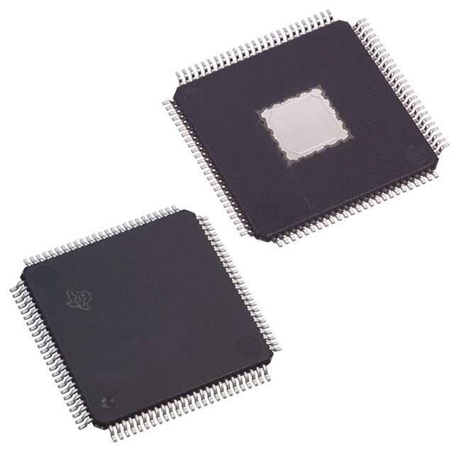
TI POWERPAD™ 100-TQFP PACKAGE
The TFP401A is packaged in TI's thermally enhanced PowerPAD™ 100TQFP packaging. The PowerPAD™
package is a 14 mm y 14 mm y 1 mm TQFP outline with 0.5-mm lead-pitch. The PowerPAD™ package has a
specially designed die mount pad that offers improved thermal capability over typical TQFP packages of the
same outline. The TI 100-TQFP PowerPAD™ package offers a back-side solder plane that connects directly to
the die mount pad for enhanced thermal conduction. Soldering the back side of the TFP401A to the application
board is not required thermally as the device power dissipation is well within the package capability when not
soldered. If traces or vias are located under the back side pad, they should be protected by suitable solder mask
or other assembly technique to prevent inadvertent shorting to the exposed back side pad.
Copyright © 2009–2011, Texas Instruments Incorporated
15
�TFP401A-EP
SLDS160A – MARCH 2009 – REVISED JULY 2011
www.ti.com
Soldering the back side pad of the device to a thermal land connected to the PCB ground plane is recommended
for electrical and EMI considerations. The thermal land may be soldered to the exposed PowerPAD™ using
standard reflow soldering techniques.
The recommended pad size for the grounded thermal land is 5.6mm sq. minimum, centered in the device land
pattern. When vias are required to ground the land, multiple vias are recommended for a low impedance
connection to the ground plane. Vias in the exposed pad should be small enough or filled to prevent wicking the
solder away from the interface between the package body and the thermal land on the surface of the board
during solder reflow.
More information on this package and other requirements for using thermal lands and thermal vias are detailed in
the TI application report PowerPAD™ Thermally Enhanced Package Application Report, TI literature number
SLMA002, available via the TI Web pages beginning at www.ti.com.
Table 1 outlines the thermal properties of the TI 100-TQFP PowerPAD™ package. The 100-TQFP nonPowerPAD™ package is included only for reference.
Table 1. TI 100-TQFP (14 X 14 X 1 mm)/0.5 mm LEAD PITCH
WITHOUT
PowerPAD™
PowerPAD™
NOT CONNECTED TO PCB
THERMAL PLANE
PowerPAD™
CONNECTED TO PCB
THERMAL PLANE (1)
Theta-JA
45°C/W
27.3°C/W
17.3°C/W
Theta-JC
3.11°C/W
0.12°C/W
0.12°C/W
Maximum power dissipation (3)
1.6 W
2.7 W
4.3 W
PARAMETER (1)
(1)
(2)
(3)
16
(2)
Specified with 2-oz. Cu PCB plating.
Airflow is at 0 LFM (no airflow)
Measured at ambient temperature, TA = 70°C.
Copyright © 2009–2011, Texas Instruments Incorporated
�TFP401A-EP
SLDS160A – MARCH 2009 – REVISED JULY 2011
www.ti.com
REVISTION HISTORY
Changes from Original (March 2009) to Revision A
Page
•
Changed 1st bullet in FEATURES: FROM: Supports UXGA Resolution (Output Pixel Rate Up to 165MHz) TO:
Supports Pixel Rates Up to 165 MHz (including 1080p and WUXGA at 60Hz) ................................................................... 1
•
Changed sentence in first paragraph of description FROM: supports display resolutions up to UXGA in 24-bit true
color pixel..TO: supports display resolutions up to 1080p and WUXGA in 24-bit true color pixel ........................................ 1
•
Changed SXGA to UXGA in paragraph, last sentence under FUNDAMENTAL OPERATION section ............................. 11
Copyright © 2009–2011, Texas Instruments Incorporated
17
�PACKAGE OPTION ADDENDUM
www.ti.com
10-Dec-2020
PACKAGING INFORMATION
Orderable Device
Status
(1)
Package Type Package Pins Package
Drawing
Qty
Eco Plan
(2)
Lead finish/
Ball material
MSL Peak Temp
Op Temp (°C)
(3)
Device Marking
(4/5)
(6)
TFP401AMPZPEP
ACTIVE
HTQFP
PZP
100
90
RoHS & Green
NIPDAU
Level-3-260C-168 HR
-55 to 125
TFP401AMPZPEP
V62/09627-01XE
ACTIVE
HTQFP
PZP
100
90
RoHS & Green
NIPDAU
Level-3-260C-168 HR
-55 to 125
TFP401AMPZPEP
(1)
The marketing status values are defined as follows:
ACTIVE: Product device recommended for new designs.
LIFEBUY: TI has announced that the device will be discontinued, and a lifetime-buy period is in effect.
NRND: Not recommended for new designs. Device is in production to support existing customers, but TI does not recommend using this part in a new design.
PREVIEW: Device has been announced but is not in production. Samples may or may not be available.
OBSOLETE: TI has discontinued the production of the device.
(2)
RoHS: TI defines "RoHS" to mean semiconductor products that are compliant with the current EU RoHS requirements for all 10 RoHS substances, including the requirement that RoHS substance
do not exceed 0.1% by weight in homogeneous materials. Where designed to be soldered at high temperatures, "RoHS" products are suitable for use in specified lead-free processes. TI may
reference these types of products as "Pb-Free".
RoHS Exempt: TI defines "RoHS Exempt" to mean products that contain lead but are compliant with EU RoHS pursuant to a specific EU RoHS exemption.
Green: TI defines "Green" to mean the content of Chlorine (Cl) and Bromine (Br) based flame retardants meet JS709B low halogen requirements of


 工商网监
湘ICP备2023018690号
工商网监
湘ICP备2023018690号
